Your browser does not fully support modern features. Please upgrade for a smoother experience.
Please note this is an old version of this entry, which may differ significantly from the current revision.
Microscopy imaging techniques are critical for the morphological characterization of thin films because they provide nanoscale structural and compositional information that impacts properties. Techniques discussed below reveal grain size, grain boundaries, surface roughness and interfaces, and defects at high resolution. When coupled with spectroscopy, microscopy may provide compositional mapping and magnetic information. This multiscale morphological information is key to elucidating structure–property relationships in thin films.
- microscopy
- diffraction
- spectroscopy
- thin magnetic films
1. Scanning Transmission Electron Microscopy (TEM)
Transmission electron microscopy (TEM) is a powerful materials characterization technique that utilizes a high-energy electron beam transmitted through a thin specimen (see Figure 1). The interactions between the incident electrons and the sample provide information about the microstructure, crystal structure, composition and electronic properties with extremely high spatial resolution. In the TEM electromagnetic optics, the high energy (100–300 keV) electrons are generated from an electron gun in the form of a thin, coherent beam that is then transmitted through tin samples. The electrons interact with the atoms of the specimen in different ways; they can be elastically scattered, partially absorbed or diffracted by crystalline planes. The transmitted electrons can be analyzed by various detectors to provide accurate information about atomic arrangement, crystalline phases and defects, allowing for the achievement of structural, chemical and electronic characterization across length scales ranging from the atomic scale crystallography to the microstructure. Advanced TEMs are capable of an atomic-scale resolution below 0.5 Å, which is especially suited to probe thin film interfaces, defects, grain structure, orientations, dislocations, and more [59,60]. However, due to the relatively short mean free path of electrons in matter, samples must be suitably prepared as thin slices, so to study thin films, it is necessary to cut thin cross-sections of the samples (cross-sectional TEM (XTEM)) using, for example, a focused ion beam (FIB) facility.
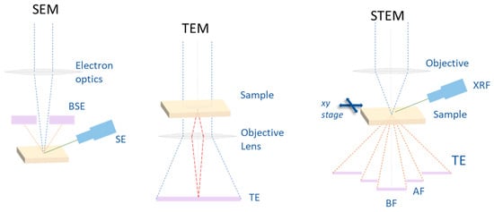
Figure 1. Main features of different electron microscopy setups. In SEM, the electron beam is focused on the sample, the image is reconstructed from secondary (SEs) and backscattered electrons (BSEs). In TEM, the sample is illuminated by a parallel electron beam, and the 2D image (transmitted electron (TE)) is formed on the detector. In STEM, the electron beam is focused on the sample, and transmitted electrons are visualized on the detectors. BF: bright field; AF: annular dark field. The X-ray fluorescence (XRF) allows for chemical maps.
In addition to conventional TEM, there are several specific applications of TEM-based techniques that can be suitably exploited for studying thin magnetic films and their interfaces. Scanning TEM (STEM) is like conventional TEM, but it scans a focused electron beam to reconstruct images. STEM can utilize different modes like bright field, dark field and high-angle annular dark field (HAADF) imaging to provide contrast based on composition, thickness, diffraction, etc. [61,62]. Energy dispersive spectroscopy (EDS) allows for chemical analysis in TEM by measuring X-rays fluorescence photons emitted when the electron beam excites atoms in the sample. This information is crucial for understanding the elemental composition, segregation, composition gradients and the presence of impurities within the film. Electron energy loss spectroscopy (EELS) analyzes energy losses of the transmitted electron beam due to inelastic scattering, thus providing chemical bonding, valence, and core-level information. It can be used to study the chemical composition, oxidation state and electronic properties of different elements in thin films. TEM electron diffraction (ED) patterns give insights into crystal structure, orientation, epitaxial relations and phase at interfaces. Convergent-beam electron diffraction (CBED) allows for the probing of the local crystallographic structure at a nanoscale resolution. High-resolution TEM (HRTEM) can directly image atomic structures, lattice spacings and defects, and can be specifically useful to resolve atomic structure at interfaces. Lorentz TEM is used to image magnetic domain structures.
2. Scanning Electron Microscopy (SEM)
It is an essential characterization tool for understanding the structural and morphological properties of magnetic thin films. SEM utilizes a focused beam of electrons to image the sample surface (see Figure 1), providing nanometer-scale resolution. When coupled with elemental analysis techniques like energy-dispersive spectroscopy (EDS), SEM enables the determination of correlating composition and morphology.
For magnetic thin films, key aspects studied via SEM include grain size, grain boundaries, film continuity and surface roughness. Grain size impacts magnetic properties like coercivity and anisotropy. Smaller grains lead to more grain boundaries, which act as pinning sites for domain wall motion, increasing coercivity. Anisotropy depends on crystal symmetry, so larger grains with fewer defects promote magnetocrystalline anisotropy. Film continuity is critical for properties like giant magnetoresistance in multilayers. Surface roughness affects domain structure and impacts magnetic behavior. SEM can also directly image magnetic domain patterns in the film when combined with electron backscatter diffraction (EBSD).
3. Time-of-Flight Secondary Ion Mass Spectrometry (ToF-SIMS)
Mass spectrometry is an analytical technique that uses a mass spectrometer to separate ions by their mass-to-charge ratio. It is a powerful yet (micro-)destructive tool that provides information about a given sample from both its surface (with an overall sensitivity of parts per million (ppm)) and bulk (with a sensitivity of part per billion (ppb)) in comparison to EDS, AES (Auger electron spectroscopy) and XPS [130]. It provides a detailed analysis of a thin film’s chemical composition, as well as interfacial characterization, and yields information about the elemental distribution in the range of a few monolayers (1–3 monolayers) through depth profiling. Furthermore, by using advanced liquid-metal ion guns (LMIGs), one can reach a lateral resolution of about 100 nm for elemental detection (ToF-SIMS imaging). The average lateral resolution obtained is <50 nm with a depth resolution of <10 nm [67,69,131,132,133,134,135,136,137]. For thin films, static ToF-SIMS is helpful to detect any kind of inhomogeneity and defects on the surface as it provides chemical maps with high sensitivity, high mass resolution (M/ΔM 10,000) and a high lateral resolution. The depth profiling can provide information regarding anomalies in the thin-film layers and the interfaces. A three-dimensional image of the composition of film is also achieved, showing the possibilities of any diffusion across the interfaces (see Figure 2).
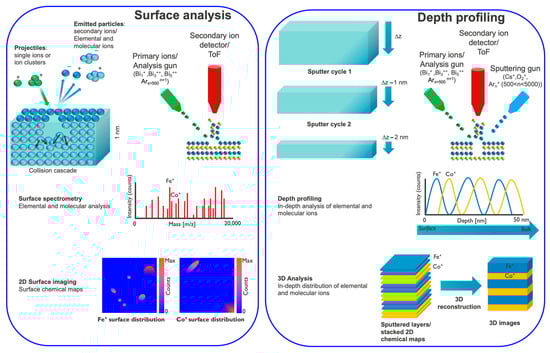
Figure 2. TOF-SIMS working principle and decoding data acquisition.
4. Spin-Polarized Low-Energy Electron Microscopy (SPLEEM)
For Low-Energy Electron Microscopy (LEEM), surfaces are imaged with the elastically backscattering of coherent low-energy electron beams that produce a high reflected electron intensity [70,138]. SPLEEM is a LEEM technique modified by the incorporation of spin-polarized GaAs-based electron gun. It is a unique and powerful tool to investigate the surface magnetic properties for low-dimensional magnetism along with in-situ measurements [70,72,139]. The basis of the magnetization sensitivity in SPLEEM is the exchange interaction between incident spin-polarized electrons and the target electrons in the magnetic sample, which provides a three-dimensional magnetic vector mapping of nanostructures. The spin-polarized incident electrons are reflected at normal incidence from the surface in a manner that depends upon the relative orientation of the spin polarization P→
of the electron beam and the local magnetization M→ in the surface layers of the sample. The reflected electrons, whose polarization is not measured, are used for imaging. The magnetic contrast (proportional to P→⋅M→) is usually superimposed on the structural contrast and can be easily disentangled using the difference between the images taken with opposite P→
values. Cathode lenses have large chromatic and spherical aberrations that limit the lateral resolution to some 101 nm. The depth resolution is, however, higher thanks to Fabry–Perot-type interferometers that allows for a thickness resolution in thin films down to the atomic scale. The main limitations of SPLEEM are that it requires crystalline materials with a strong preferred crystal orientation that can produce a specular beam along the optical axis of the microscope to achieve a suitable resolution.
SPLEEM has been used to address aspects of magnetic domain and domain wall structure in thin magnetic films and surface-supported nanostructures [140,141,142,143], exchange coupling in ferromagnetic/nonferromagnetic sandwiches [144,145] and spin reorientation transition in Co layers or Fe/Ni bilayers [146,147]. SPLEEM has also been used to study spin-dependent electron reflectivity and spin-resolved quantum well resonances in ferromagnetic Fe and Co magnetic thin films [148,149].
5. Photoemission Electron Microscopy (PEEM)
Photoemission Electron Microscopy (PEEM) is a powerful imaging technique. It combines photoelectron spectroscopies with microscopic techniques and is specifically useful to study thin magnetic films and interfaces [150,151,152,153,154]. PEEM was initially developed with laboratory sources (UV), but brilliant soft X-ray synchrotron sources allow for greater element specificity. The basic of PEEM technique involves exciting the sample with UV or soft X-ray and providing an image of the position from which the photoelectrons emerge from the sample. Owing to the relatively short photoemitted electron mean free path, PEEM is mainly a close-to-surface (2–5 nm depth) sensitive technique. The spatial resolution limits the aberrations in the electron optics as well as the electron mean free paths in the few ten nm range. Magnetic sensitivity is obtained using a polarized incoming beam, making PEEM sensitive to the spin and orbital occupancy of the electronic states close to the sample surface. In the soft X-ray energy range, being 200–2000 eV, absorption is dominated by electronic transitions to unfilled 3d (transition metals) or 4f (rare earths) bands where the magnetism originates, making the photoelectrons very sensitive to the magnetism of the sample. When circularly polarized radiation is used, the X-ray circular magnetic dichroism (XMCD) effect, originating from the unbalanced filling of spin-up and spin-down states, provides additional sensitivity to the magnetic state of the sample [155,156].
6. Atomic Force Microscopy (AFM)
Atomic force microscopy (AFM) has become an indispensable tool for the characterization and development of thin-film materials and devices, allowing for the wide probing of several surfaces and interfaces properties with nanoscale resolution. In AFM, a sharp tip on the end of a flexible cantilever scans across the sample surface while deflections of the cantilever are measured (Figure 3). These deflections correspond to tip-sample interaction forces that allow for the generation of topological images of the sample surface. AFM is ideally suited for characterizing thin films and buried interfaces as it can probe nanoscale morphology, surface roughness, friction, magnetism, electrical properties, and more [157,158,159,160]. Operating modes such as contact, tapping, and non-contact AFM allow for the optimized imaging of delicate samples. Key strengths include the ability to map topological and material variations with nanometer resolution, measure extremely weak forces, and conduct the in situ imaging of samples during processing. Advanced AFM techniques can provide compositional mapping, phase contrast, electronic structure, and even sub-molecular resolution on suitable samples.
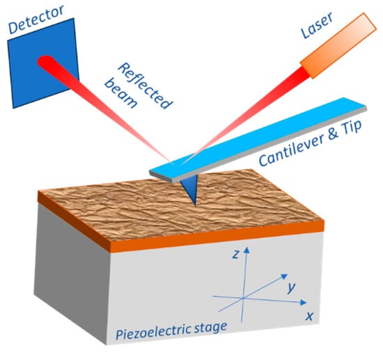
Figure 3. Working principle of AFM. It utilizes a tiny cantilever with a sharp tip at one end. The deflection of the cantilever is recorded looking at the reflection of the laser beam and is used to create a map of the surface morphology.
The main use of AFM is for surface topography. It can provide high-resolution images of thin films, revealing their surface roughness, grain boundaries and other surface features. By analyzing the height profile obtained from AFM images, the film thickness can be determined with nanometer-level precision. This is particularly useful for monitoring the growth or deposition process of thin films. By analyzing the force field, AFM can map the nanomechanical properties of thin films, such as their elastic modulus, adhesion and hardness. By exploiting different modes of AFM, such as force spectroscopy or nanoindentation, the local mechanical response of the film can be measured. This information is crucial for understanding the film’s behavior under different conditions and for optimizing its performance.
Advanced AFM modes provide specific applications addressed to study magnetic nanostructures, giving a wealth of information critical for understanding the magnetic behavior of these thin films and interfaces. Magnetic force microscopy (MFM) is a specialized AFM mode that detects long-range magnetic forces between a magnetic tip and the sample surface. This method allows for the imaging of magnetic domain structures down to some 101 nm scale resolution. Magnetic exchange force microscopy (MExFM) directly provides 2D maps describing the variation of magnetic exchange coupling strength. In this technique, a non-magnetic tip is used, and the interaction between the probe and the sample arises from the magnetic exchange coupling between the probe and the magnetic sample. The spin-polarized scanning tunneling microscopy (SP-STM) uses a magnetic tip to probe magnetic states with atomic resolution. It can directly observe nanoscale spin textures at surfaces and interfaces. Furthermore, 2D magnetic imaging can be performed while simultaneously applying electric or magnetic fields to reveal dynamic switching behavior. High-resolution AFM techniques can directly observe domain wall structure, pinning, and motion at surfaces and buried layers.
This entry is adapted from the peer-reviewed paper 10.3390/ma16237331
This entry is offline, you can click here to edit this entry!