Your browser does not fully support modern features. Please upgrade for a smoother experience.
Please note this is an old version of this entry, which may differ significantly from the current revision.
Subjects:
Materials Science, Coatings & Films
Researchers prepared composite conductive inks with high conductivity, high thermal conductivity, strong stability, and excellent comprehensive mechanical properties by combining carbon-based materials such as graphene and carbon nanotubes with metal-based materials. Through new electronic printing technologies, conductive inks can be used not only to promote the development of integrated circuits but also in various new electronic products.
- integrated circuits
- electronic printing
- conductive ink
- graphene
- carbon nanotubes
1. Conductive Mechanism of Conductive Inks
Conductive ink is a functional electronic material consisting of a viscous ink mixture with a conductive function produced by uniformly dispersing the conductive functional phases in the carrier solvent, adding additives, and a certain amount of binder [10]. The prepared conductive ink is transferred to the substrate using different electronic printing methods [11]. After removing the nonconductive carrier solvent and the additive using low-temperature curing [12], high-temperature sintering [13], laser irradiation [14], and other postprocessing means, the volume of the conductive ink shrinks and the conductive functional phases are closely connected to form a conductive network, which can form a conductive pathway under the action of an external voltage to achieve conductive function [15]. The conductive mechanism of conductive inks is quite complex, and the microscopic and macroscopic levels are usually applied with different conductive mechanisms. So far, there are three main conductive mechanisms that are widely acknowledged by the academic community: the conductive channel mechanism, the tunneling effect theory, and the field emission effect.
1.1. Conductive Channel Mechanism
The conductive channel mechanism refers to the conductive channels in the conductive ink, which are formed by the direct contact of numerous conductive particles, resulting in the conductive behavior [16]. Before sintering, conductive particles in the organic carrier of the conductive ink are isolated from each other without the capacity to conduct electricity; during the sintering process of the conductive ink, the nonconductive organic carrier decomposes and volatilizes as the temperature increases, and the adhesive phase melts and contracts after absorbing heat, wetting the conductive functional phase and pulling the conductive functional phase to orderly rearrange through surface tension to achieve the conductive function, as displayed in Figure 1. The conductive channel mechanism, also known as percolation theory, is applicable to the macroscopic explanation of the system with a large percentage of conductive particles added [17]. Via continuously increasing the proportion of conductive particles added to the conductive ink up to a certain amount, the conductive particles that originally dispersed individually in the conductive ink contact each other to form tightly connected chainlike channels that can conduct electricity in all directions, thus substantially enhancing the conductive properties of the conductive ink [18]. There is a special value that indicates the percolation threshold for the addition of conductive particles. The percolation threshold depends on the type of conductive particles, organic carrier, bonding phase, and dispersion state in the conductive ink. The percolation threshold represents the minimum value for which high electrical conductivity via the conduction mechanism occurs. After the percolation threshold, the conductivity would continue to increase by one or more orders of magnitude as a function of filler loading. The printability and as-printed mechanical properties suffer if the loading gets too high. The optimal loading level may be different for diverse materials, applications, and printing techniques. The concentration of conductive particles in metal-based conductive inks often lies between 30% and 80%, and the high-temperature-resistant organic or inorganic chemicals are often chosen to be adhesives [19]. The concentration between 30% and 40% is suitable for inkjet printing. The concentration between 50% and 80% is usually used in screen printing due to the high viscosity. The conductive particle contents of polymer-based conductive ink are between 5% and 30% [20,21]. Polymer-based conductive ink is commonly used to print circuits using inkjet printing technology due to its low concentration. Due to the hydrophobic and agglomerative character of the carbon-based materials, the solids content of the carbon-based materials is usually varied in the range of 2% to 10% [22,23,24]. The concentration of graphene in carbon-based materials for screen printing can be as high as 10%, while its concentration for other printing methods is limited in the range of 2%–6%. To strengthen the conductivity, the solid content of conductive particles was improved from 10% to 30% through the formation of carbon-based composite ink with other excellent conductive metals or polymers [25,26,27]. A solids content of carbon-based composites of 30% is usually applied in screen printing, and a solids content of around 10% is suitable for other printing technologies.
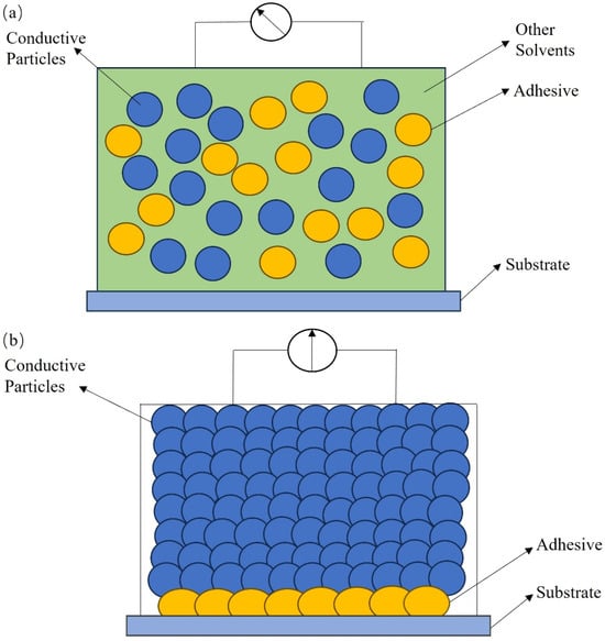
Figure 1. Diagram of conductive particles in conductive ink before and after sintering: (a) before sintering; (b) after sintering.
1.2. Tunnel Effect Theory
The conductive channel mechanism explains the conductive phenomenon at the macroscopic level but cannot explain the following phenomena: even if massive conductive particles are exceedingly close together, microscopic gaps still exist, resulting in a low probability for conductive particles to make direct contact with each other in order to constitute complete conductive paths. In addition, because of the existence of nonconductive organic carriers and bonding components in the system, the conductive particles cannot form an isotropic chain to build three-dimensional conductive paths; therefore, the electrons will not be conducted through direct contact between the conductive particles. The theory of the tunneling effect argues that direct contact with conducting particles is not a necessary condition to constitute a conducting channel [28]. In quantum mechanics, when the distance between conducting particles is less than 10 nm, under the action of the applied electric field, electrons can shuttle and jump between conducting particles to shape a large tunneling current accompanied by thermal vibrations, thus completing the construction of a conducting channel. The tunneling effect theory is suitable for situations where the concentration of conductive particles is low and the conductive pathway cannot be constituted by direct contact between conductive particles.
1.3. Field Emission Effect
The field emission effect occurs when the solid content of the conductive particles in the ink is extremely low and the conductive particles remain discontinuous in the carrier solvent after curing. However, under the action of an applied high electric field, there is an electric potential difference between the electric fields of two conductive particles adjacent to each other, so that the internal electrons of the conductive particles gain energy to escape across the surface potential barrier and come into contact with the neighboring conductive particle, and thus, conductivity is finally achieved by the escape of electrons inside the particles [29].
Figure 2 reveals the conductive model diagram for different conductive mechanisms, where RL indicates the resistance of conductive particles in contact with each other, C manifests the capacitance of the insulating layer formed by factors such as the distance of conductive particles and the nonconductive components in the ink, Rg illustrates the resistance of the current path due to the tunneling effect, and Cg demonstrates the capacitance of the current path due to the tunneling effect. RE indicates the current path resistance due to the field emission effect, and CE represents the current path capacitance due to the field emission effect. Rd indicates the resistance due to a tiny fraction of conductive particles in contact with each other. When the concentration of conductive particles is high, the conductive particles easily make contact with each other, and therefore, the probability of three-dimensional conductive mesh channels shaped in the conductive ink is higher. The conductive channel mechanism (percolation theory) dominates, as manifested in the type 1 conductive mechanism model in Figure 2. When the concentration of conductive particles is too low to establish effective contact for most conductive particles, which maintain the status of single or small clusters distributed in the ink system, the conductive particles are in relatively close proximity to each other, only separated by a very narrow insulating layer formed by organic carriers and other polymers. The quantum mechanical tunneling effect theory is the dominant mechanism, as indicated in the type 2 conductive mechanism model in Figure 2. When the proportion of conductive particles is minuscule but the applied voltage is high, the field emission effect plays a significant role in conducting electricity, as manifested in the type 3 conductive mechanism model in Figure 2. When the percentage of conductive particles is extremely low and the applied electric field is also relatively minor, the tunneling effect or field emission effect cannot operate between the conductive particles, resulting in the insulation of the conductive ink, as shown in the type 4 conductive mechanism model in Figure 2. In a complex conductive ink system, at the micro and macro levels, the three mechanisms tend to coexist and interact with each other to promote electron transport in the conductive film layer.
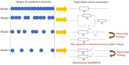
Figure 2. Conductive mechanism models in conductive ink.
2. Classification of Conductive Inks
The classification of conductive inks is multitudinous. According to the curing method of conductive inks, they can be divided into low-temperature curing [12], high-temperature sintering [13], chemical sintering [30], photonic curing [31], and microwave and plasma sintering [32]. In terms of various printing modes, they can be categorized into screen printing, gravure printing, flexographic printing, and inkjet printing. In accordance with the conductive phase for classification, conductive inks can be classified as metal-based, polymer-based, carbon-based, and composite systems. As the conductive functional phase is the core component of conductive ink, which determines the final electrical properties of the conductive ink, this article mainly introduces the types of conductive ink in detail based on the different conductive functional phases.
2.1. Metal-Based Conductive Ink
Metal-based conductive ink is ink composed of Au, Ag, Cu, Al, or their alloys as conductive functional phases. Gold conductive ink has good conductivity and strong oxidation resistance, but its high cost limits its application. The research on silver-based conductive ink is relatively mature. Because of its excellent conductivity and resistance to oxidation, silver conductive ink has been widely used. However, the drawbacks are also obvious, such as high cost, long-term exposure to high current density, and high-temperature environments that can lead to electromigration [33], which do not meet the preparation requirements and application conditions of large-scale integrated circuits. Copper is a metal with electrical conductivity second only to silver in nature. Copper powder not only possesses excellent resistance to electromigration but also has a low cost due to its wide range of sources. However, copper nanopowder is prone to oxidation, and in practical applications, it is necessary to conduct oxidation-resistance treatment on the surface of copper powder. As the preparation of integrated circuits requires a high volume of raw materials with excellent conductivity and low cost, the current research on metal-based conductive inks for integrated circuits is mainly focused on copper-based conductive inks and their antioxidation preparation process. Min et al. prepared a copper complex conductive ink using copper formate as a precursor and isopropanol (IPA) as solvent [34]. The conductive copper ink was coated on an indium tin oxide (ITO)-coated glass substrate using a spin-coating method, which was selectively sintered using a nanosecond pulsed ultraviolet laser. Subsequently, the excess conductive ink beyond the solidified pattern was washed with IPA solution, resulting in a circuit with a minimum line width of 10 μm. The conductivity was up to 1.14 × 10⁶ S·m−1. Cheng et al. used copper hydroxide as a precursor, polyvinylpyrrolidone (PVP) as a capping agent, and ascorbic acid as a reducing agent to prepare antioxidant copper nanoparticles with a particle size of around 150 nm, and they selected tert-butanol and ethanol with a volume ratio of 90% and 10% as solvents, respectively. Finally, copper conductive ink was sintered in a muffle furnace at 250 °C for 120 min to obtain copper conductive films with conductivity as high as 5.9 × 10⁶ S·m−1 [19]. Hwang et al. configured copper nanopowder with polyvinylpyrrolidone (PVP) and mono-diethylene glycol (DEG) to form a copper conductive ink, which was then coated on a polyimide substrate and sintered with a white flash; the process was optimized by varying the energy of the white flash and using the assistance of deep UV and near-IR irradiation [35]. The results indicated that the maximum conductivity of the pattern after sintering with deep-UV-assisted white flash was 1.3 × 10⁷ S·m−1. Del et al. demonstrated that the surface coating of copper nanopowders with organic amines can form a passivation layer to prevent oxidation and agglomeration of copper nanopowders as well as to reduce the sintering temperature of the ink by adjusting the composition and ratio of the carrier solvent [36]. Mou et al. dispersed extremely tiny copper powder particles with a particle size of 6.5 nm into isopropanol amine (IPA) and ethylene glycol solutions to prepare copper conductive ink that can achieve low-temperature bonding of copper and that has self-reduction characteristics [37]. The stabilizer IPA enabled the copper ink to have self-reduction properties, which can effectively prevent the oxidation of copper nanoparticles and significantly reduce the sintering temperature. The copper ink was subjected to low-temperature sintering under an Ar gas atmosphere with a temperature of 250 °C. The contact between Cu-Cu particles could construct a metallurgical bond to obtain Cu-Cu joints with a shear strength of 36.2 MPa. The self-reduction and sintering process, illustrated in Figure 3, possesses great potential for application in three-dimensional IC packaging. Li et al. cleaned copper nanopowder in formic acid solution to remove the oxide layer on the surface of the powder and, subsequently, dispersed the cleaned copper nanopowder into a solution of isopropyl alcohol amine (IPA), butanol, and methanol to obtain copper ink [38]. The copper nanopowder prepared using this method had better antioxidant properties and conductivity. After sintering, the conductive copper film was denser, with an electrical conductivity of 2 × 10⁷ S·m−1, which was twice or three times higher than the solid copper, showing a great prospect for applications in chip packaging.
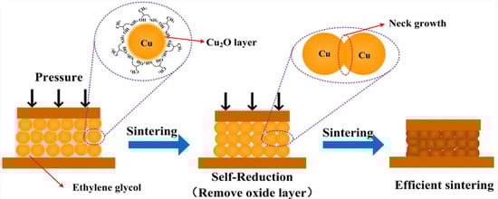
Figure 3. Schematic diagram of the self-reducing and sintering process of conductive Cu ink [37].
The above research demonstrates that copper powder can effectively avoid being oxidized and the sintering temperature can be reduced by using different organic amines to wrap around the surface of the copper powder in copper conductive inks, thus allowing the application of affordable conductive copper ink to replace gold and silver conductive inks. This approach fulfills the production requirements of large-scale integrated circuits through the utilization of laser irradiation [39], vacuum sintering, and other curing methods [40]. The prepared conductive copper ink with excellent antioxidation, electrical conductivity, and mechanical properties can completely satisfy the high requirements of integrated circuits for electrical and mechanical properties, reliability, and low-cost conductive materials. Furthermore, this method can also be applied in the preparation of conductive films, chip packaging, and electronic packaging of three-dimensional integrated circuits.
2.2. Polymer-Based Conductive Ink
The conductive functional phase of the polymer-based conductive ink is achieved with the use of polymers with electrical conducting ability, which are a group of organic polymers with a long chain structure of conjugated π-bonds and metal-like electrical properties in the doped state that retain their original organic polymer properties [41]. Frequently utilized conductive polymers are polythiophene (PTh), polyaniline (PANI), polypyrrole (PPy), poly(3,4-ethylenedioxythiophene) (PEDOT), poly(3,4-ethylenedioxythiophene)/poly(styrene sulfonate) (PEDOT/PSS), etc. PANI has the advantages of high electrical conductivity, excellent stability, simple structure, competitive price, solubility in most organic solvents, etc., thus becoming a widely capitalized polymer. PEDOT possesses high electrical conductivity, flexibility, and optical transparency. PEDOT/PSS is a mixture of poly(3,4-ethylenedioxythiophene) and polystyrene sulfonate, which has superior electrical conductivity, dispersibility, and processability. Due to the insolubility of PEDOT, its application in conductive inks is limited. PSS is a water-soluble polymer that can be combined with PEDOT via electrostatic interaction; therefore, doping PSS in PEDOT can facilitate its solubility. Corletto et al. distributed the powder of PEDOT/PSS in a solvent consisting of water, ethanol, and dimethylformamide (DMF) to prepare ink, then poured the conductive ink into a die with low-surface-energy dimethyl siloxane (PDMS) using a topographical discontinuous dewetting formula, and finally transferred the circuit pattern onto the Si wafer substrate via the liquid bridge transfer measure after inverting the die [20]. The circuit pattern shrank after the sintering process because of the removal of excess solvent and cosolvent. The average conductivity of the treated IC pattern was up to 1.19 × 10⁵ S·m−1, and the lateral circuit resolution was capable of reaching about 400 nm, which was higher than the conductivity and printing resolution of most of the reported polymer-based conductive inks. Zeng et al. utilized carboxymethylcellulose sodium (CMC) as a raw material to prepare PEDOT-CB/CMC composites via in situ polymerization, which were attached with aqueous polyurethane dispersion (PUD) as the solvent and CMC as a binder. The prepared conductive ink was applied to screen printing to evaluate its printability [42]. It was concluded that the addition of nanoscale conductive carbon black as a doping agent in the preparation of PEDOT-CB/CMC ink successfully enhanced the electrical conductivity and stability of the ink while also acting as a carrier material for the polymerization of PEDOT and strengthening the dispersion performance of PEDOT in aqueous solution. CMC, as a dispersant and binder, also further improved the dispersion and rheology of PEDOT.
However, in comparison with metal nanoparticles, polymers have inferior conductivity and complex synthesis processes, and it is difficult to make polymers soluble in most organic solvents [43]. The progress is relatively slow in the research of polymer-based conductive ink due to the poor electrical conductivity of conductive polymers and the obstacle of finding matching conventional solvents that can provide stable storage of conductive ink. Polymer-based conductive ink is mainly fabricated by compounding with other, higher-conductive materials to increase conductivity, while the addition of water-soluble polymers to ink promotes its solubility.
2.3. Carbon-Based Conductive Ink
Conductive functional phases of carbon-based conductive ink consist of graphite, carbon black, and newly discovered carbon materials such as graphene and carbon nanotubes. The traditional carbon conductive functional phase includes carbon black, graphite, carbon fiber, etc., with the advantages of reasonable cost, stable chemical properties, and favorable resistance stabilities. However, the shortcomings, such as high resistivity and poor humidity resistance, make it hard to satisfy the demands of integrated circuits on the capacities of printed circuits. Due to their unique structures, graphene and carbon nanotubes exhibit superior properties compared with other carbon materials. These new carbon materials can be ideally utilized in modern high-power integrated circuits because of their characteristics, such as high carrier mobility and high thermal conductivity, as well as high tensile strength and excellent resistance to electromigration [44,45,46]. Gao et al. used ultrasonic-assisted supercritical CO2 to exfoliate graphite to obtain the initial graphene flakes [47]. Through this preparation method, the structure of graphene is less prone to damage and can maintain high electrical conductivity. The graphene was dispersed by using 0.1% (w/v) ethyl cellulose (EC) and cyclohexanone, which greatly alleviated the graphene agglomeration due to the hydrophobic interaction between ethyl cellulose and graphene to counteract the van der Waals forces. The prepared conductive ink could be stored stably for more than 9 months. The conductive film was printed several times with an inkjet printing method and sintered at 300 °C for 30 min to attain the conductivity of 9.24 × 10³ S·m−1, while the pattern was satisfactorily flexible and its resistivity increased slightly after bending and folding 1000 times. Secor et al. used ethanol as a solvent, which was cheaper and more environmentally friendly than the solvent used in conventional liquid-phase exfoliation, combined with ethyl cellulose as a stabilizer to produce high-performance graphene from graphite via liquid-phase exfoliation [22]. Then, graphene–EC powder was obtained using the following centrifugation and flocculation steps. An amount of 2.4 wt% graphene–EC powder was distributed in an 85:15 cyclohexanone/terpineol solution in order to obtain a low-viscosity conductive ink with a surface tension of 33 mN/m, which could achieve stable droplet formation in inkjet printing. The conductivity of the printed film layer was 2.5 × 10⁴ S·m−1 after a low-temperature curing process of annealing at 250 °C for 30 min. The high viscosity of ink contributes to the reduction in the ink-flaring phenomenon after printing; thus, it can increase the resolution of printed circuit patterns. Secor et al. dispersed graphene–EC powder in a mixture of ethanol and terpineol, which allowed rapid and complete dispersion [23]. By promoting the solid content of graphene and adjusting the ratio of solvents, the viscosity of the ink can be effectively improved, thus reducing the spread of the ink after printing and achieving the purpose of improving the printing resolution. The resolution of printed circuits could be optimized by reducing the size of the smallest printing cell and increasing the viscosity of the ink. Continuous lines with fine resolution of 20~30 μm and conductivity of about 104 S·m−1 were achieved using such a process, which was the first time that the application of graphene conductive ink to large areas and highly precise patterns in gravure printing was realized. Preparation of graphene by conventional liquid-phase exfoliation requires the addition of excessive amounts of dispersants or surface modifiers to facilitate the exfoliation of graphene and prevent its aggregation. In order to solve the above problems, Choudhury et al. used poly[2-(3-thienyl)ethyloxy-4-butylsulfonate] sodium salt (PTEBS) to exfoliate graphite to obtain graphene via liquid-phase exfoliation without adding excessive dispersants to facilitate exfoliation and prevent aggregation of graphene [24]. PTEBS is an electrically conductive molecule consisting of a heterocyclic aromatic ring (thiophene moiety) and additional sodium sulfonate functional groups. The sodium sulfonate group makes PTEBS soluble in water, while the thiophene group allows it to interact with graphene, resulting in a stable dispersion of graphene in aqueous solutions. Successful exfoliation and stabilization of graphene by this method will allow the emergence of self-dispersible pristine graphene and provide an opportunity for further processing into dry, water-dispersible graphene powders. Highly concentrated aqueous graphene inks (up to 10 mg/mL) have been formulated for printing flexible conductive circuits, showing excellent conductivity without heat treatment. In addition, Choudhury prepared aqueous dispersions of poly(3-hexylthiophene-2,5-diyl) (P3HT) nanoparticles using a simple microemulsion process and used them as a medium for graphite exfoliation, where interfacial interactions between the P3HT nanoparticles and graphene were exploited to simultaneously stabilize the exfoliated graphene flakes and induce efficient intermolecular charge transfer [48]. The correlated π-electrons of P3HT can strongly interact with the dispersed π-electrons of two-dimensional (2D) graphene, thus inducing highly efficient charge transfer and enhancing the electrical conductivity of graphene. Nanoparticle-stabilized graphene (G/P3HT) dispersions were used to print flexible conductive circuits with square resistances up to 180 Ω·sq−1.
Graphene, carbon nanotubes, and other carbon-based conductive materials have excellent mechanical, electrical, thermal, corrosion, and electromigration resistance. A comparison of the performance characteristics of these carbon materials is listed in Table 1. Although these carbon-based materials are prone to agglomeration with poor dispersion, which reduces conductivity, the preparation of high-performance carbon-based conductive inks can be achieved by adapting the preparation process and adjusting the composition of the solvent. In order to reduce the use of excessive dispersants and increase the hydrophilicity of graphene, aromatic polymers can be used in the preparation of graphene using the liquid-phase exfoliation method. To enhance the electrical conductivity of graphene, conjugated conductive polymers can be added during the preparation of graphene, and the π-electrons of conjugated polymers can strongly interact with the dispersed π-electrons of two-dimensional (2D) graphene, effectively promoting charge transfer. The integrated circuit patterns can be printed on a flexible or rigid substrate via screen printing, inkjet printing, or other electronic printing technologies using carbon-based conductive ink to generate flexible conductive films and high-resolution integrated circuit patterns, which are expected to break through the current challenges faced by integrated circuit materials in terms of high conductivity, thermal conductivity, outstanding strength and reliability, etc.
Table 1. Comparative properties of carbon materials.
2.4. Composite Conductive Ink
Composite conductive ink is a kind of conductive ink prepared by combining the conductive functional phases of diverse systems or various characteristic materials in the same system. It is generally divided into carbon/metal composite conductive ink, carbon/polymer conductive ink, and conductive ink composed of different metals. Although the electrical properties of silver ink are excellent, the high cost limits its application in the manufacture of large-scale integrated circuits. In order to reduce the cost while improving their electrical properties, Li et al. employed an in situ reduction method to fabricate graphene-bridged silver conductive inks [25]. Cysteamine was chosen as the molecular bridging agent, with one end anchored to the graphene surface via the diazonium reaction and the other end linked to the silver atoms via the thiol functional group to achieve molecular-scale bridging between graphene and silver, thus facilitating the charge transfer at the graphene/silver interface. The results revealed that the maximum conductivity of the prepared graphene-bridged silver conductive ink was capable of attaining 2 × 10⁵ S·m−1, and the printed circuit patterns exhibited high conductivity and excellent flexibility. Graphene could replace some of the silver nanoparticles and promote the longitudinal transfer of electrons between graphene and silver nanoparticles, enhancing the electrical conductivity while diminishing the amount of precious-metal silver and reducing the production cost.
Although graphene possesses high carrier mobility, the low carrier density is another intrinsic electrical property of graphene. In order to enhance the carrier density of graphene, chemical doping of graphene can make electrons transfer in or out of graphene to cause the generation of extra electrons/holes in graphene molecules, leading to n-type/p-type doping of graphene [51]. Therefore, Liu et al. achieved p-type doping of graphene with CuCl2 using the liquid-phase reaction method [52]. To prevent the agglomeration of graphene flakes through steric hindrance, polymers play a crucial role in graphene-based conductive ink by improving rheological properties and storage performance. In the subsequent preparation process, the composite conductive ink was prepared with the acquired CuCl2-doped graphene and carbon black as the composite conductive functional phase for retaining the polymers to possess excellent rheological properties, divalent acid ester (DBE) as the organic solvent, and polyurethane as the adhesive polymer, which achieved a conductivity of 3.13 × 10⁴ S·m−1 for the printed patterns. For the purpose of simplifying the preparation process, CuCl2 was directly added to the graphene conductive ink in the subsequent preparation process, and the same p-type doping of graphene in the ink system was achieved. Because carbon black was applied as an auxiliary conductive phase without removing polymers, the conductivity of printed patterns still attained 3.64 × 10⁴ S·m−1 with exceptional mechanical properties [26].
The reliable stability and extremely hydrophobic nature of graphene limit the application of water-based inks. The oxygenated groups of graphene oxide (GO) can effectively enhance its hydrophilicity and enable further chemical modification and functionalization, but the oxidation process damages its original structure and diminishes its electrical and mechanical properties. Restoring an extensive sp2 carbon network with excellent electrical properties while maintaining high hydrophilicity could be the appropriate functionalization approach in order to produce reduced graphene oxide (rGO) [53]. Giasafak et al. prepared carbon-based composite materials consisting of rGO and silver nanowires (AgNWs) through a physical mixture and an in situ reduction method [54]. The functionalization of the graphene sheets with amino and aryl sulfonic groups was achieved by adding 2,4-diaminobenzenesulfonic acid (DBSA) in the process of reduction, which could generate a positive effect on the electrical properties and water dispersibility. The mixing at the physical level allowed the AgNWs to be well dispersed and anchored onto the surface of rGO, resulting in a highly interconnected three-dimensional network that leads to enhanced surface conductivity. The in situ reduction method enabled the composite conductive inks to demonstrate better electrical properties. The conductivity of the conductive pattern prepared via the in situ reduction method could attain 7.4 × 10⁴ S·m−1. This is mainly attributed to the surface modification of AgNWs and graphene oxide by DBSA, which led to the covalent attachment on the surface of the rGO rather than surface adsorption in the physical mixture.
In contrast to the single-carbon-based conductive ink, the composite conductive phases were qualified to incorporate the advantages of various systems of conductive phases. By using approaches such as in situ reduction or chemical doping, more conductive channels can be constructed between metal conducting particles and graphene to enhance the electrical properties of conductive inks, while the introduction of polymers can effectively modify the rheological properties of the system to suit the electronic printing process. Through appropriate graphene oxidation and reduction processes, the hydrophilicity of graphene can be elevated for the preparation of aqueous conductive inks for more application areas, and its high conductivity can be maintained by preserving the sp2 carbon network structure. Meanwhile, the covalent attachment between rGO and other metal nanowires can effectively promote its overall electrical properties by constructing a three-dimensional conductive network. As a consequence, composite conductive ink provides superior electrical and thermal properties as well as high tensile strength and excellent resistance to electromigration, which can be an ideal choice for composite materials for integrated circuits. Therefore, composite conductive ink has enormous potential to be the material of first choice for the preparation of new electronic packaging materials, heat exchange materials of electronic components, and integrated circuit lead frames in the future.
This entry is adapted from the peer-reviewed paper 10.3390/coatings13101769
This entry is offline, you can click here to edit this entry!