Inventions in Additive Manufacturing Processes: History
Please note this is an old version of this entry, which may differ significantly from the current revision.
Additive Manufacturing (AM), also known as 3D Printing (3DP), has emerged as a transformative technology revolutionizing various industries including very demanding ones such as the aerospace and biomedical industries.
  • additive manufacturing
  • invention
  • holistic review
  • 3D printing
  • multi material
  • beam-based metal
  • stereolithography
  • bioprinting
  • two-photon polymerization
  • hybrid technologies
  • open-source

1. Introduction

In recent years, additive manufacturing (AM) has witnessed significant advances in terms of technology, materials, and applications. Recent AM technology inventions that have the potential to revolutionize the field of AM and beyond. The following trends in AM development are considered as break-through innovations:

High-Speed Sintering (HSS): HSS is a powder bed fusion (PBF) technology that uses infrared heating to selectively sinter polymer powders. It enables faster production speeds and has the potential for the large-scale manufacturing of functional polymer parts. Loughborough University has pioneered and patented the innovative HSS technology, which revolutionizes the 3DP process by enabling the cost-effective, high-volume production of intricate and customizable parts [1]. HSS competes favorably with injection molding in terms of economic feasibility. Various industries, such as the aerospace, automotive, consumer goods, healthcare, and medical industries, have embraced HSS within their end-product supply chains [2][3][4]. Moreover, an increasing number of global brands have embraced HSS as their preferred method for product creation.
Continuous Liquid Interface Production (CLIP): CLIP is a resin-based 3DP technology based on the original SLA/DLP process, which uses light and oxygen to selectively cure a liquid resin into solid parts continuously. It offers fast printing speeds and can produce parts with smooth surface finishes [5].
Laser Powder Bed Fusion (L-PBF) Enhancements: L-PBF, a widely used metal AM technique, has seen advancements in process monitoring and control such as melt pool monitoring, optical tomography or layer deposition/scanning monitoring, multi-laser processing technology, and new materials. These innovations have led to improved part quality, reduced porosity, enhanced mechanical properties, and increased production efficiency [6][7].
Directed Energy Deposition (DED) with wire and powder feedstock: DED techniques have been expanded to include the use of powder feedstock in addition to wire feedstock. This allows for the deposition of a wider range of materials, including metals, ceramics, and composites, enabling greater design flexibility and the production of large-scale parts. Moreover, hybrid manufacturing combining subtractive and DED AM technologies has provided unique opportunities such as an improved surface quality and dimensional accuracy in internal features of large AM components [8].

2. Multi-Material AM

Multi-Material and Functionally Graded AM: Advances have been made in the development of AM techniques capable of printing multi-material and functionally graded structures. These technologies allow for the incorporation of different materials or variations in material properties within a single printed part, expanding the range of applications and enabling complex designs [9]. Advances in multi-material AM technologies have allowed for the simultaneous deposition of different materials, enabling the creation of complex objects with varying mechanical, electrical, and optical properties. Multi-material AM has broad applications in fields such as the healthcare, electronics, and aerospace fields [10][11]. A voxel level is the smallest unit of a three-dimensional digital model, analogous to a pixel in a two-dimensional image. By controlling the material composition and properties of each voxel, AM can create objects with unprecedented complexity and functionality. A team of researchers from MIT developed a multi-material AM system that can print with up to eight different materials at a resolution of 50 µm per voxel [12]. The system uses an array of micro-nozzles to deposit droplets of photopolymer resin onto a moving platform, which are then cured by ultraviolet light. This technique can create objects with varying stiffness, transparency, color, and conductivity within a single print.

Multi-material AM holds significant potential and addresses the growing need for functional product design [13]. Traditional manufacturing techniques often face limitations in producing complex, customized designs that require multiple materials with distinct properties. However, with multi-material AM, designers can overcome these constraints and create functional products with enhanced performance and versatility [14]. By seamlessly integrating different materials within a single print, varied functionalities can be incorporated, such as mechanical strength, electrical conductivity, flexibility, and transparency, into their designs. This capability opens up new possibilities for industries ranging from aerospace and automotive to electronics and all Internet of Things (IoT) markets. Moreover, multi-material AM enables the optimization of material usage, reducing waste and cost while increasing design efficiency. As industries strive for greater innovation, customization, and performance, the demand for multi-material AM continues to grow, highlighting its immense potential for driving advancements in functional product design [15].
One of the modern examples of successful multi-material AM is Nano Dimension technology [16]. Nano Dimension is a company that specializes in the development of AM solutions for the production of electronic devices. Their technology, known as DragonFly, enables the 3DP of functional electronic circuits and components, including multi-layer PCBs (Printed Circuit Boards) and other intricate electronic structures. The DragonFly system combines the inkjet deposition of conductive and dielectric inks with a precise layer-by-layer printing process. It allows for the creation of complex, high-resolution electronic designs, including prototypes, custom circuitry, and small-scale production runs. Multi-material AM offers advantages such as rapid prototyping, design flexibility, and the ability to embed electronic components directly into 3D-printed structures. The applications of Nano Dimension’s 3DP technology include research and development, aerospace, defense, automotive, and various other industries that require advanced electronics manufacturing capabilities.
Nano Dimension’s DragonFly system enables multi-material printing by combining different types of inks. The specific combination of materials used depends on the desired application and the requirements of the printed electronic circuit or component. Here are some examples of materials that can be used in multi-material printing with the DragonFly system [17]:
Conductive inks: These inks are used to print conductive traces, pads, and interconnects. They typically contain metallic particles such as silver or copper that provide electrical conductivity.
Dielectric inks: Dielectric inks are used to create insulating layers and barriers between conductive elements. These inks have high electrical resistance and are crucial for isolating different circuit components.
Insulating inks: Insulating inks are used to create non-conductive structures, such as mechanical support or protective enclosures. They provide structural integrity to the printed object.
Functional inks: In addition to conductive and dielectric inks, functional inks can be used to incorporate specific properties into printed electronics. For example, magnetic or optical inks can be employed to add functionalities like sensors or antennas.
It is important to note that Nano Dimension’s technology allows for the combination of various materials, enabling the creation of complex multi-layered electronic circuits with different functionalities and characteristics. The specific combination of materials depends on the desired design and functionality of the printed electronic device.
There have already been several papers published researching the potential of the Nano Dimension solution for various functional 3DP. For example, the work of Yang et al. [18] highlights the utilization of this solution based on piezoelectric additive fabrication for the production of single-substrate multi-metal-layer antennas. By vertically stacking metal layers in a 3D-printed single substrate, the designed antennas demonstrate wide bandwidth and ultra-low-profile advantages. The study includes the design, fabrication, and measurement of multi-layer linear polarization (LP) patch antenna elements and LP antenna arrays. The results show that the proposed LP patch antenna improves the impedance bandwidth significantly compared to traditional single-layer LP patch antennas. Additionally, the integration of the feeding network into the same substrate without increasing the size or profile of the array is demonstrated. Circular polarization (CP) patch antennas and CP antenna arrays are also fabricated and measured, showcasing wider impedance bandwidth and a broader frequency range. These antennas, designed for sub-6 GHz frequencies, exhibit great potential for applications in 5G consumer mobile electronics, combining an ultra-low profile and wideband capabilities. Sokol et al. [19] explore the use of AM technology for designing and producing planar capacitors as part of electronic circuit boards. The capacitors are constructed as pairs of conductive plates with varying geometries and layers, allowing for a wide range of capacitance values, from picofarads to nanofarads. The performance of these additively manufactured capacitors is shown to surpass that of commercially available surface mount device (SMD) capacitors by up to 20 GHz. They exhibit high breakdown voltages exceeding 1 kV and minimal leakage currents in the subpicoampere range. Additionally, the change in the RF impedance with the frequency is significantly smaller compared to that of SMD capacitors, with a reduction of three times. This demonstrates the superior performance and potential of Nano Dimension’s AM technology for producing high-quality, high-performance capacitors for electronic applications.

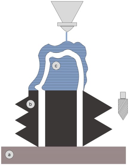
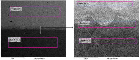
3. Beam-Based Metal AM

Beam-based metal AM processes have gained significant recognition in various industries due to their immense potential. However, achieving the full industrialization of these processes still requires further efforts. To promote the industrialization of metal AM, numerous companies, research centers, and universities have been investing in comprehensive research and development activities [20].
This part focuses on the progress of metal AM technologies by examining patents. Using the Orbit Intelligence database, a search was conducted specifically for beam-based metal AM patents. The analysis began by studying the number of patents per year, revealing a substantial growth in AM patenting activities, as anticipated. Further examination of the patents aimed to identify the key players in the field. It was discovered that multidisciplinary companies, AM machine producers, end users (especially in the aerospace sector), universities, and research centers were the main contributors to this market [21].
In beam-based AM, there are several approaches for producing innovative multi-material and graded structures. The first approach to producing functionally, structurally, and compositionally graded structures in PBF was proposed via using blended powders. The application of such powder blends together with smart scanning strategies results in the possibility of producing graded microstructures. For example, Lakhdar et al. produced materials like Damascus steel with a ductile core and abrasive surface using such approach [22].
The Aerosint company, established in 2016, proposed another novel technology known as “Selective Powder Deposition” (SPD). This innovative approach enables the targeted deposition of multiple powders to form a single layer comprising two or more distinct materials. In contrast to conventional powder bed processes that utilize single-material rollers or blade recoaters, Aerosint’s SPD presents an alternative solution. The applicability of this technology extends to various AM techniques, including L-PBF, Binder Jetting, and Pressure Assisted Sintering. By offering a versatile solution for selective powder deposition, Aerosint’s SPD technology has the potential to enhance the capabilities and expand the possibilities of these AM processes. This innovative approach enables the selective deposition of multiple materials within a single layer of a 3D-printed object. Unlike traditional multi-material 3DP methods that typically rely on the mixing or sequential deposition of materials, Aerosint’s technology allows for the precise and simultaneous deposition of different materials in a single layer. The Aerosint technology utilizes a specialized recoating system that can selectively deposit a range of powders onto the build platform. By controlling the deposition process, different materials can be placed in specific areas or patterns within a layer, enabling the creation of complex multi-material structures. This capability leads to new possibilities for designing and fabricating functional parts with graded material properties, localized variations, or the integration of dissimilar materials. By enabling the combination of multiple materials in a single AM process, it offers the ability of incorporating functionalities such as conductivity, strength, flexibility, or corrosion resistance within a single part.

4. Stereolithography and Microwave Sintering

One groundbreaking invention in AM is the fusion of stereolithography and microwave sintering. By using stereolithography to 3D-print objects with powdered materials and subsequently subjecting them to microwave sintering, this innovation enables the creation of complex and accurate objects with a reduced processing time. The combination of these techniques allows for the rapid consolidation and densification of the printed parts while offering a wide range of material options. This advancement expands the capabilities of AM, revolutionizing the production of intricate, functional, and diverse objects [23].
As one of the inventions in this area, the following example can be provided: Continuous Liquid Interface Production (CLIP). CLIP is a resin-based 3DP technology that uses light and oxygen to selectively cure a liquid resin into solid parts continuously. CLIP is an exclusive 3DP technique that was patented in 2014 by Carbon3D, formerly known as EiPi Systems [24]. Falling within the category of vat polymerization, CLIP shares similarities with the older stereolithography (SLA) and digital light processing (DLP) methods. Another term used to describe CLIP is digital light synthesis (DLS), both denoting the same innovative approach to 3DP.
In CLIP, a liquid photopolymer resin is selectively exposed to ultraviolet (UV) light, causing it to solidify and form parts. Although it may resemble SLA and DLP, CLIP distinguishes itself as a continuous process that eliminates the discrete steps of earlier printing methods. The breakthrough of CLIP lies in its implementation of an oxygen-permeable membrane, which creates a zone beneath the part known as a “persistent liquid interface”. This interface allows for uninterrupted curing as the part is progressively drawn out of the resin. Instead of using a layer-by-layer approach, CLIP employs a digital projector and microcontrollers to project a dynamically changing image of the 3D model, streamlining the printing process into a layer-less design.
CLIP offers several advantages over other printing methods:
  • Remarkable speed: CLIP prints achieve the same accuracy and surface quality as DLP/SLA prints but are completed 100 times faster.
  • Superior surface finish: The layer-less nature of CLIP prints enhances their surface quality, making them comparable to parts produced through injection molding.
  • Exceptional properties: CLIP parts are watertight and fully isotropic (exhibiting equal strength in all orientations) and possess increased strength compared to SLA/DLP prints.
  • Versatility for prototyping and production: CLIP parts can be used for functional prototyping and are even suitable for full production runs.
  • Structural integrity: This is CLIP’s ability to easily integrate variable cell structures within a single part to produce different performance characteristics.
  • Versality: CLIP/DLS printers offer a wide range of material options that are distinct from many other printer types.
This demonstrates that even the oldest and most well-known SLA technology still has potential for further inventions and development.

5. Bioprinting and Tissue Engineering

This subsection focuses on the concept of 3D bioprinting, a specific branch of AM that can be defined as the production of complex biological constructs using living cells, biomolecules, and biomaterials. Similar to inkjet-based 3DP methods, 3D bioprinting is also developed based on 2D inkjet printers by replacing ink in the cartridge with biological material (bioinks) and paper with biodegradable support material. Currently, only a few 3DP methods (MEX, inkjet printing, and laser printing) are suitable for bioprinting technology.
Bioprinting is an AM technique that uses living cells as the building blocks to create tissue-like structures for biomedical applications. Tissue engineering is a field that aims to create functional tissues and organs for transplantation or drug testing. A team of researchers from Rice University developed a bio-AM technique that integrates bioprinting and tissue engineering [20]. The technique uses a bio-ink composed of stem cells, blood vessels, and hydrogel to print vascularized tissue constructs. The technique can create tissue constructs with complex shapes and sizes, such as bone, cartilage, skin, and livers [25][26][27].
3D bioprinting is a promising research direction and is highly relevant in terms of economic efficiency. According to the Grand View Research report, the 3D bioprinting market was valued at USD 1.4 billion in 2020, and it is expected to grow at a compound annual growth rate of 15.8% from 2021 to 2028 [28]. By 2024, the 3D bioprinting market is projected to account for approximately 10% of the total 3DP market. Furthermore, the global tissue engineering market was valued at USD 2 billion in 2019 and is expected to reach USD 7 billion by 2027 [28].
It is worth noting that scaffold-based approaches, which involve framework-like beam structures, still face some challenges such as difficulties in uniform cell seeding, limited vascularization, and weak cell adhesion to the scaffold material. Therefore, living cells themselves or in combination with bioactive molecules and biomaterials need to be incorporated into a 3D scaffold for successful tissue or organ engineering [29].
The further expansion of 3D bioprinting finds its justification in the demand within medical sectors such as cosmetics and pharmaceuticals. The high demand for organ transplantation and the shortage of available organs are key factors driving the development of 3D bioprinting strategies aimed at reducing waiting times, the need for immunosuppression, and donor organ compatibility. This demand is expected to increase due to the large population of individuals over the age of 60 worldwide, who have a lower level of immunity and are more prone to accidents [30].

6. Two-Photon Polymerization

Two-photon polymerization (TPP) in AM has found diverse applications in various fields. For instance, in microelectronics, TPP enables the creation of complex microstructures such as photonic crystals and microelectromechanical systems (MEMS). These structures have unique optical and mechanical properties, making them valuable in miniaturized devices and sensors. In optics, TPP has been utilized to fabricate high-quality micro-optical components like lenses, waveguides, and diffraction gratings. These components exhibit precise control over light propagation and find applications in optical communications and imaging systems.
In the field of tissue engineering, TPP has enabled the production of intricate scaffolds with tailored architectures, which can support the growth and organization of cells for regenerative medicine applications. Additionally, TPP has been applied in microfluidics to create microchannels, valves, and pumps, enabling the precise manipulation and control of fluids at the microscale. The versatility of two-photon polymerization has led to its exploration and adoption in numerous fields, where the ability to fabricate complex, high-resolution micro- and nanostructures is crucial for advanced applications [31].

7. Hybrid Technologies

The concept of hybrid AM originated from the recognition that combining traditional subtractive manufacturing with AM could overcome the limitations of both processes, offering a novel approach for mass-producing medium- to large-sized components with high geometric complexity and accuracy. Lately, there have been a high number of hybrid AM practices cited; a few of them are presented below:
  • Steel-based materials have witnessed significant advancements through PBF and directed energy deposition (DED) techniques, with notable efforts made to produce steel-based hybrid and composite materials using PBF methods [32].
  • The integration of DED techniques with traditional computer numerical control (CNC) machining processes offers enhanced flexibility, enabling applications in hybrid manufacturing, protective coatings, and parts repair.
  • Laser-based PBF enables hybrid AM, where a simple-shaped substrate component is conventionally manufactured, while a complex-shaped part is directly printed onto it, e.g., the build of the part with conformal cooling onto an existing bulk mold.
There have been recent advancements in hybrid AM technologies, where two or more manufacturing techniques are combined to fabricate 3D objects. One such hybrid AM method combines additive processes with subtractive methods such as milling or machining (see Figure 1). This approach enables the efficient fabrication of complex parts by leveraging the advantages of both additive and subtractive technologies. As a result, production is accelerated, and surface finishes are improved [33].
Figure 1. Schematic view of hybrid manufacturing, where (a) stands for the building platform, (b) stands for the machined part, and (c) stands for the printed part with complex inner cooling.
In Figure 2 below, the microstructure of the hybrid AM part are shown where the bottom wrought part was produced via subtractive manufacturing from H13 steel, and the top part was additively manufactured from MAR C300 steel using the L-PBF process. One can observe the diffusion of these steels from one to another and the corresponding change in the chemical composition in the interface zone. The relatively deep diffusion and blending of the initial chemical compositions of the steels result in an increased strength of the interface and, in general, an increased strength of the hybrid component [34].
Figure 2. SEM image of the gradient structure in the interface area of the hybrid-AM part [34].
In a study referenced in [35], a concept of hybridization in AM was explored. Specifically, the potential of using a PBF-fabricated part on a wrought substrate was investigated as a hybrid wrought–AM manufacturing route for Ti-6Al-4V damage critical load-bearing components. The researchers examined hybrid specimens, where the AM part was produced via selective laser melting (SLM), focusing on microstructural variations, defect presence, uniaxial tensile ductility, and fracture toughness across various configurations. It was observed that defects were present in both the AM part and the wrought counterpart of the specimens, with no discernible differences in their characteristics.
This hybrid approach combines the benefits of additive and subtractive manufacturing, integrating AM into the traditional production chain to compensate for the limitations of AM processes and ultimately advancing the industrialization of AM. Moving forward, continued research and development in hybrid AM hold the potential to revolutionize manufacturing practices by enabling the efficient production of intricate, high-quality components on a larger scale.
Binder Jetting printing assisted with traditional heat post-processing exemplifies hybrid manufacturing [36][37]. In this approach, AM is utilized solely for shape production by printing a green body, while traditional powder metallurgy methods, such as sintering and liquid metal infiltration, are employed to achieve the desired densification, microstructure, and mechanical or physical properties [38][39][40][41]. This combination of AM and post-processing techniques proves advantageous for the manufacturing of functional parts and the design of composites [42][43]. By leveraging the strengths of both processes, this hybrid approach enables the production of components with tailored properties and complex geometries that may be challenging to achieve through conventional manufacturing methods alone. The utilization of binder jetting and traditional heat post-processing in synergy expands the possibilities for creating advanced materials and functional parts with enhanced performance characteristics [40][41]. Further research and development in this field hold promise for optimizing the hybrid manufacturing process and broadening its applications across various industries.

8. Open-Source Inventions in AM

Open-Source Inventions in AM refer to the technologies that are developed and shared within the open-source AM community. These inventions are characterized by their open nature, allowing anyone to access, modify, and distribute the designs, software, and documentation associated with the technology. Open-Source in AM encourages collaboration and knowledge sharing among individuals and organizations, fostering a community-driven approach to technological advancement. It enables individuals to build upon existing ideas, modify designs to suit their specific needs, and contribute back improvements or new ideas to benefit the entire community.
Open-Source AM has several advantages over traditional, proprietary approaches to technology development. First, it encourages collaboration and knowledge sharing among individuals and organizations. This can lead to faster innovation, as ideas can be freely exchanged and built upon. Second, open-source AM is more democratic, as anyone can participate in the development process. This can help to ensure that the technology is developed in a way that meets the needs of the wider community. Third, open-source AM is more sustainable, as it reduces the need for closed, proprietary systems.
On this topic, Joshua Pearce of Western University has a high number of unique contributions [44][45]. In one of his latest inventions, his team made an open-source walker, which is a customizable device, whereby the joints are additively manufactured on desktop machines and the tubing is cut to size. The goal of the project is to make a walker that is both open-source and customizable, as well as cost-effective [46].
The following list provides some of the popular Open-Source Inventions reported in recent years:
  • RepRap: RepRap is one of the earliest and most well-known open-source AM projects [47]. It focuses on the development of self-replicating 3D printers, which are capable of producing most of their own components. The RepRap community has contributed to advancements in the field and has made it more accessible to a wider audience.
  • Prusa i3: The Prusa i3 is a popular open-source 3D printer design created by Josef Prusa [48]. The design has been iterated upon and improved by the community, resulting in various versions and modifications. The Prusa i3 design has been widely adopted and has played a significant role in making 3D printing more affordable and accessible.
  • Marlin Firmware: Marlin is an open-source firmware that controls and operates 3D printers [49]. It supports a wide range of 3D printer models and provides features such as the precise control of stepper motors, temperature regulation, and support for various file formats. Marlin firmware has been continuously developed and improved by the open-source community, enabling 3D printer users to customize and optimize their machines.
  • Slic3r: Slic3r is an open-source slicing software used in AM [50]. It takes 3D models and converts them into instructions (G-code) that a 3D printer can understand. Slic3r provides advanced options for customizing print settings and optimizing the printing process. The open-source nature of Slic3r has allowed for community contributions, resulting in new features, bug fixes, and improved performance.
Open-source innovations have played a vital role in driving the advancement and accessibility of AM technology. Through promoting collaboration and the exchange of knowledge, these groundbreaking inventions have expedited innovation, broadened accessibility, and empowered individuals and communities to explore and create novel applications for AM. Open-Source AM has the potential to accelerate innovation, democratize technology, and make AM more sustainable. As the AM community continues to grow, open-source AM is likely to play an increasingly important role in the development of this technology.

This entry is adapted from the peer-reviewed paper 10.3390/inventions8040103

References

  1. Nonaka, K.; Takeuchi, N.; Morita, T.; Pezzotti, G. Evaluation of the effect of high-speed sintering on the mechanical and crystallographic properties of dental zirconia sintered bodies. J. Eur. Ceram. Soc. 2023, 43, 510–520.
  2. Tan, X.; Lu, Y.; Gao, J.; Wang, Z.; Xie, C.; Yu, H. Effect of high-speed sintering on the microstructure, mechanical properties and ageing resistance of stereolithographic additive-manufactured zirconia. Ceram. Int. 2022, 48, 9797–9804.
  3. Williams, R.J.; Al-Dirawi, K.H.; Brown, R.; Burt, J.; Bayly, A.E.; Majewski, C. Correlations between powder wettability and part colour in the High Speed Sintering process. Addit. Manuf. 2021, 47, 102361.
  4. Solodkyi, I.; Bogomol, I.; Loboda, P. High-speed electron beam sintering of WC-8Co under controlled temperature conditions. Int. J. Refract. Met. Hard Mater. 2022, 102, 105730.
  5. Lipkowitz, G.; Samuelsen, T.; Hsiao, K.; Lee, B.; Dulay, M.T.; Coates, I.; Lin, H.; Pan, W.; Toth, G.; Tate, L.; et al. Injection continuous liquid interface production of 3D objects. Sci. Adv. 2022, 8, 3917.
  6. Zhao, X.; Wang, T. Laser Powder Bed Fusion of Powder Material: A Review. In 3D Printing and Additive Manufacturing. 2022. Available online: https://home.liebertpub.com/3dp (accessed on 1 June 2023).
  7. Guerra, M.G.; Lafirenza, M.; Errico, V.; Angelastro, A. In-process dimensional and geometrical characterization of laser-powder bed fusion lattice structures through high-resolution optical tomography. Opt. Laser Technol. 2023, 162, 109252.
  8. Ahn, D.-G. Directed Energy Deposition (DED) Process: State of the Art. Int. J. Precis. Eng. Manuf. Technol. 2021, 8, 703–742.
  9. Han, D.; Lee, H. Recent advances in multi-material additive manufacturing: Methods and applications. Curr. Opin. Chem. Eng. 2020, 28, 158–166.
  10. New 3D Printer Promises Faster, Multi-Material Creations|Stanford News. Available online: https://news.stanford.edu/2022/09/28/new-3d-printer-promises-faster-multi-material-creations/ (accessed on 4 June 2023).
  11. Shaukat, U.; Rossegger, E.; Schlögl, S. A Review of Multi-Material 3D Printing of Functional Materials via Vat Photopolymerization. Polymers 2022, 14, 2449.
  12. Overview ‹ Making Data Matter: Voxel-Printing for the Digital Fabrication of Data across Scales and Domains—MIT Media Lab. Available online: https://www.media.mit.edu/projects/making-data-matter/overview/ (accessed on 4 June 2023).
  13. Hasanov, S.; Gupta, A.; Nasirov, A.; Fidan, I. Mechanical characterization of functionally graded materials produced by the fused filament fabrication process. J. Manuf. Process. 2020, 58, 923–935.
  14. Hasanov, S.; Gupta, A.; Alifui-Segbaya, F.; Fidan, I. Hierarchical homogenization and experimental evaluation of functionally graded materials manufactured by the fused filament fabrication process. Compos. Struct. 2021, 275, 114488.
  15. Loy, J.; Novak, J.I.; Scerri, M.; Chowdhury, M.H.H.; Skellern, K. Developing Transition Research for Disruptive Technology: 3D Printing Innovation. 2021, 1–20. Available online: https://services.igi-global.com/resolvedoi/resolve.aspx?doi=10.4018/978-1-7998-4303-0.ch001 (accessed on 15 May 2023).
  16. Nano Dimension 2023 About Nano Dimension. Available online: https://www.nano-di.com/about-nano-dimension (accessed on 16 June 2023).
  17. Persad, J.; Rocke, S. Multi-material 3D printed electronic assemblies: A review. Results Eng. 2022, 16, 100730.
  18. Li, M.; Yang, Y.; Iacopi, F.; Nulman, J.; Chappel-Ram, S. 3D-Printed Low-Profile Single-Substrate Multi-Metal Layer Antennas and Array With Bandwidth Enhancement. IEEE Access 2020, 8, 217370–217379.
  19. Sokol, D.; Yamada, M.; Nulman, J. Design and Performance of Additively Manufactured In-Circuit Board Planar Capacitors. IEEE Trans. Electron Devices 2021, 68, 5747–5752.
  20. Additive Manufacturing|TRUMPF. Available online: https://www.trumpf.com/en_US/solutions/applications/additive-manufacturing/?gclid=Cj0KCQjw7PCjBhDwARIsANo7CgmvBY8WHxwX9dxzXknktMapcMU05kCW3S3XoxOEwQXiYfd32cfsHrAaAvuiEALw_wcB (accessed on 4 June 2023).
  21. Aversa, A.; Saboori, A.; Marchese, G.; Iuliano, L.; Lombardi, M.; Fino, P. Recent Progress in Beam-Based Metal Additive Man-ufacturing from a Materials Perspective: A Review of Patents. J. Mater. Eng. Perform. 2021, 30, 8689.
  22. Koptyug, A.; Popov, V.V.; Vega, C.A.B.; Jiménez-Piqué, E.; Katz-Demyanetz, A.; Rännar, L.-E.; Bäckström, M. Compositionally-tailored steel-based materials manufactured by electron beam melting using blended pre-alloyed powders. Mater. Sci. Eng. A 2019, 771, 138587.
  23. Lakhdar, Y.; Tuck, C.; Binner, J.; Terry, A.; Goodridge, R. Additive manufacturing of advanced ceramic materials. Prog. Mater. Sci. 2021, 116, 100736.
  24. Thomas Supplier Discovery Platform All about Continuous Liquid Interface Production 3D Printing. Available online: https://www.thomasnet.com/articles/custom-manufacturing-fabricating/continuous-liquid-interface-production-3d-printing/ (accessed on 16 June 2023).
  25. Grigoryan, B.; Paulsen, S.J.; Corbett, D.C.; Sazer, D.W.; Fortin, C.L.; Zaita, A.J.; Greenfield, P.T.; Calafat, N.J.; Gounley, J.P.; Ta, A.H.; et al. Multivascular networks and functional intravascular topologies within biocompatible hydrogels. Science 2019, 364, 458–464.
  26. Multimaterial 3D Printing with a Twist. Available online: https://seas.harvard.edu/news/2023/01/multimaterial-3d-printing-twist (accessed on 4 June 2023).
  27. Derakhshanfar, S.; Mbeleck, R.; Xu, K.; Zhang, X.; Zhong, W.; Xing, M. 3D bioprinting for biomedical devices and tissue engineering: A review of recent trends and advances. Bioact. Mater. 2018, 3, 144–156.
  28. 3D Bioprinting Market Size, Share & Trends Analysis Report by Technology (Magnetic Levitation, Inkjet-Based), by Application (Medical, Dental, Biosensors, Bioinks), by Region, and Segment Forecasts, 2023–2030; Grand View Research: San Francisco, CA, USA, 2023.
  29. Popov, V.V.; Kudryavtseva, E.V.; Katiyar, N.K.; Shishkin, A.; Stepanov, S.I.; Goel, S. Industry 4.0 and Digitalisation in Healthcare. Materials 2022, 15, 2140.
  30. Bartolo, P.; Malshe, A.; Ferraris, E.; Koc, B. 3D bioprinting: Materials, processes, and applications. CIRP Ann. 2022, 71, 577–597.
  31. O’Halloran, S.; Pandit, A.; Heise, A.; Kellett, A. Two-Photon Polymerization: Fundamentals, Materials, and Chemical Modification Strategies. Adv. Sci. 2023, 10, 2204072.
  32. Ozsoy, A.; Tureyen, E.B.; Baskan, M.; Yasa, E. Microstructure and Mechanical Properties of Hybrid Additive Manufactured Dissimilar 17-4 PH and 316L Stainless Steels. Mater. Today Commun. 2021, 28, 102561.
  33. Pragana, J.; Sampaio, R.; Bragança, I.; Silva, C.; Martins, P. Hybrid metal additive manufacturing: A state–of–the-art review. Adv. Ind. Manuf. Eng. 2021, 2, 100032.
  34. Popov, V.V.; Fleisher, A. Hybrid additive manufacturing of steels and alloys. Manuf. Rev. 2020, 7, 6.
  35. Dolev, O.; Osovski, S.; Shirizly, A. Ti-6Al-4V hybrid structure mechanical properties—Wrought and additive manufactured powder-bed material. Addit. Manuf. 2021, 37, 101657.
  36. Lv, X.; Ye, F.; Cheng, L.; Fan, S.; Liu, Y. Binder jetting of ceramics: Powders, binders, printing parameters, equipment, and post-treatment. Ceram. Int. 2019, 45, 12609–12624.
  37. Popov, V.; Fleisher, A.; Muller-Kamskii, G.; Avraham, S.; Shishkin, A.; Katz-Demyanetz, A.; Travitzky, N.; Yacobi, Y.; Goel, S. Novel hybrid method to additively manufacture denser graphite structures using Binder Jetting. Sci. Rep. 2021, 11, 2438.
  38. Du, W.; Ren, X.; Ma, C.; Pei, Z. Ceramic binder jetting additive manufacturing: Particle coating for increasing powder sinterability and part strength. Mater. Lett. 2019, 234, 327–330.
  39. Polozov, I.; Razumov, N.; Masaylo, D.; Silin, A.; Lebedeva, Y.; Popovich, A. Fabrication of Silicon Carbide Fiber-Reinforced Silicon Carbide Matrix Composites Using Binder Jetting Additive Manufacturing from Irregularly-Shaped and Spherical Powders. Materials 2020, 13, 1766.
  40. Fleisher, A.; Zolotaryov, D.; Kovalevsky, A.; Muller-Kamskii, G.; Eshed, E.; Kazakin, M.; Popov, V. Reaction bonding of silicon carbides by Binder Jet 3D-Printing, phenolic resin binder impregnation and capillary liquid silicon infiltration. Ceram. Int. 2019, 45, 18023–18029.
  41. Li, L.; Tirado, A.; Conner, B.; Chi, M.; Elliott, A.M.; Rios, O.; Zhou, H.; Paranthaman, M.P. A novel method combining additive manufacturing and alloy infiltration for NdFeB bonded magnet fabrication. J. Magn. Magn. Mater. 2017, 438, 163–167.
  42. Gupta, A.; Hasanov, S.; Fidan, I. Processing and Characterization of 3d-Printed Polymer Matrix Com-Posites Reinforced with Discontinuous Fibers. In Proceedings of the 2019 International Solid Freeform Fabrication Symposium, Austin, TX, USA, 12–14 August 2019.
  43. Gupta, A.; Fidan, I.; Hasanov, S.; Nasirov, A. Processing, mechanical characterization, and micrography of 3D-printed short carbon fiber reinforced polycarbonate polymer matrix composite material. Int. J. Adv. Manuf. Technol. 2020, 107, 3185–3205.
  44. Joshua Pearce|Opensource.com. Available online: https://opensource.com/users/jmpearce (accessed on 13 July 2023).
  45. Petsiuk, A.; Pearce, J.M. Towards smart monitored AM: Open source in-situ layer-wise 3D printing image anomaly detection using histograms of oriented gradients and a physics-based rendering engine. Addit. Manuf. 2022, 52, 102690.
  46. So, A.; Reeves, J.M.; Pearce, J.M. Open-Source Designs for Distributed Manufacturing of Low-Cost Customized Walkers. Inventions 2023, 8, 79.
  47. Rayna, T.; Striukova, L.; Fauchart, E. Commercialization Strategies of Large-Scale and Distributed Open Innovation: The Case of Open-Source Hardware. Calif. Manag. Rev. 2023, 65, 22–44.
  48. Hu, B. Original Prusa i3: The Self-Replicating 3D Printer. Oper. Manag. Educ. Rev. 2023, 15, 5–22.
  49. Montes, E.; Lasmarias, G.; Escanilla, E.J.; Velasco, L.C. Conversion of Proprietary 3D Printer for Open-Source Utilization. Lect. Notes Netw. Syst. 2022, 217, 343–355.
  50. Anand Sankar, M.; Deepak Lawrence, K.; Mathew, J. Part Quality Improvement of Fused Filament Fabrication-Based Additive Manufacturing by Means of Slicing Software Modifications. Lect. Notes Mech. Eng. 2023, 251–265.
More
This entry is offline, you can click here to edit this entry!
ScholarVision Creations