When cooling a superconductor in a magnetic field below the transition temperature, Tc, the material characteristically tries to expel the magnetic flux due to the induced shielding currents (often also called Meissner currents). When measuring the magnetic moment, m(T), in this situation a diamagnetic signal (m = negative) appears. This so-called Meissner-Ochsenfeld effect is one of the two hallmarks of superconductivity besides the zero resistance and represents the strongest proof if a material is a true superconductor. However, in the literature there are also superconducting materials which show an appearing paramagnetic (positive m) signal below Tc when measuring m(T) in small applied magnetic fields. This so-called Paramagnetic Meissner Effect (PME) or Wohlleben effect was first observed in bulk, Bi2Sr2CaCu2O8 high- Tc superconducting (HTSc) materials, and subsequently as big surprise also in conventional Nb superconductors. Since then, PME was found in many more metallic and HTSc materials, having various shapes (bulks, crystals, thin films), and various aspect ratios and compositions, including multilayers and doped materials. Thus, our paper reviews all the experimental aspects of the PME.
- superconductivity
- PME
- Meissner effect
- metallic superconductors
- flux trapping
- Giant vortex state
Topic review
Paramagnetic Meissner Effect (PME)
Subjects: Condensed matter physics, Superconductivity
Submitted by:
Michael Koblischka, L. Pust, C.-S. Chang, T. Hauet, A. Koblischka-Veneva
Definition
When cooling a superconductor in a magnetic field below the transition temperature, Tc, the material characteristically tries to expel the magnetic flux due to the induced shielding currents (often also called Meissner currents). When measuring the magnetic moment, m(T), in this situation a diamagnetic signal (m = negative) appears. This so-called Meissner-Ochsenfeld effect is one of the two hallmarks of superconductivity besides the zero resistance and represents the strongest proof if a material is a true superconductor. However, in the literature there are also superconducting materials which show an appearing paramagnetic (positive m) signal below Tc when measuring m(T) in small applied magnetic fields. This so-called Paramagnetic Meissner Effect (PME) or Wohlleben effect was first observed in bulk, Bi2Sr2CaCu2O8 high- Tc superconducting (HTSc) materials, and subsequently as big surprise also in conventional Nb superconductors. Since then, PME was found in many more metallic and HTSc materials, having various shapes (bulks, crystals, thin films), and various aspect ratios and compositions, including multilayers and doped materials. Thus, our paper reviews all the experimental aspects of the PME.
1. Introduction
The superconducting state is characterized by two hallmarks: the vanishing electrical resistance [1] below the superconducting transition temperature, Tc, and the Meissner-Ochsenfeld effect [2], describing the expulsion of magnetic flux from the superconducting sample when cooling it in an applied magnetic field (field cooling, FC), creating a diamagnetic state with negative magnetization, m. This implies that the induced screening currents try to expel the magnetic flux from the sample. The implications of the Meissner-Ochsenfeld effect led directly to the development of the basic theories of superconductivity (London, Ginzburg-Landau and BCS), and are intensively described in all textbooks on superconductivity (see, e.g., [3-10]). Thus, the first observations of superconducting transitions of Bi-based, high-Tc superconductors (HTSc) to a paramagnetic state (positive magnetization m, attracting magnetic field) instead of a diamagnetic one were more treated as experimental mishaps and went mostly unnoticed by the community [11,12]. The situation changed with more detailed measurements on granular Bi2Sr2CaCu2O8 (Bi-2212) samples by Braunisch et al., linking the observation of a superconducting transition in field-cooling m(T)-curves towards the paramagnetic state with unique features of the HTSc, i.e., the so-called d-wave superconductivity and effects of granularity (π-junctions between the grains) [13,14]. This was soon followed by other researchers, applying also different measurement techniques to exclude possible experimental artifacts and providing some theories to explain these observations Following these works, several theoretical approaches were published concerning this effect, now named paramagnetic Meissner effect (PME) or Wohlleben effect [15]. The key element of the PME is thus the observation of positive magnetization (attracting magnetic field) upon field-cool cooling (FC-C) or warming (FC-W) in m(T)-measurements as shown in Figs. 1 (a)—(c).
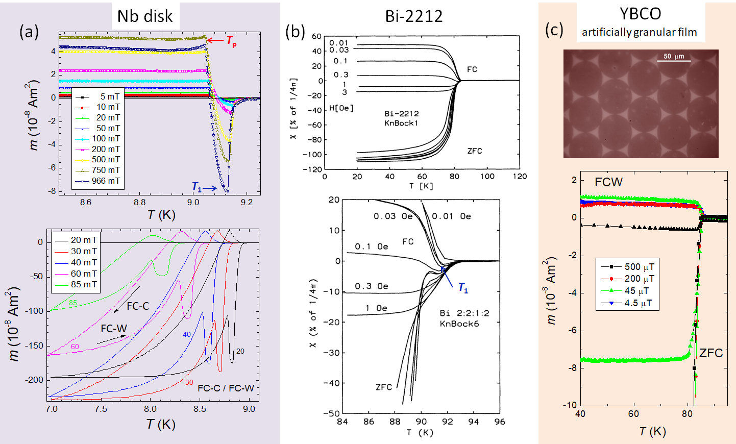
Figure 1. Comparison of the experimentally observed PME effect in 3 different types of superconductors. (a). PME in a bulk Nb disk. In the upper graph, the recorded field-cool warming (FC-W) curves are given for small magnetic fields (5 μT -- 966 μT). The lower graph gives both FC-C and FC-W curves with the applied fields given alongside the respective curves. The arrows indicate the measurement direction. Note here the characteristic minima (T1) and maxima (Tp), which are visible up to the highest applied fields. Reprinted with permission from [16]. (b). PME in a HTSc Bi-2212 polycrystalline, bulk sample. The upper plot shows the field-cool cooling (FC-C) data together with the zero-field cooling (ZFC) curves for several applied magnetic fields. The lower graph of (b) presents the transition region in more detail. Reprinted with permission from [13,14]. (c). PME observed in an artificially granular HTSc YBCO thin film [x], see the image of the sample in the upper graph. The lower graph gives the FC-W and ZFC curves obtained on this type of sample. This is an example with no surface superconductivity, and the positive m(T)-signal is entirely due to the trapped flux in the open spaces between the disks. Reprinted with permission from [17].
Thus, it came as a big surprise as Thompson [16,18] presented an observation of PME on bulk niobium disks, a classical s-wave superconductor, or often called conventional or low-Tc superconductor (LTSc). This work was soon followed by Kostic et al. [19] presenting a thorough investigation of the PME in Nb materials. This work resulted in a comment [20] and a reply [21], where the inherent differences between the PME in metallic, s-wave superconductors and the HTSc (d-wave superconductors) were clarified. Furthermore, several reports presented details of the superconducting transitions on different Nb samples with the magnetic field applied in parallel and perpendicular directions [22], the vanishing of the PME by surface treatments [23] and the enhancement of the PME by ion implantantion [24]. In this way, a new research direction was born.
The mostly isotropic LTSc used for these studies were compact, bulk and homogeneous materials in stark contrast to HTSc that are typically granular materials with their inherent complicated crystal structures, mostly tetragonal ones. Therefore, the LTSc may serve -- owing to their relative simplicity -- as a superconducting model system to perform detailed studies in order to clarify the physical origin of the paramagnetic moment appearing when crossing through Tc from higher temperatures. Since then, the PME was observed in a variety of metallic superconductors and in different forms like thin films, nanowire arrays, multilayer systems and very importantly, in nanocomposites, and mesoscopic structured samples Multilayered materials may be composed of superconductor/normal metal, but also superconducting/para- or ferromagnetic ones. Of course, since the discovery of MgB2 -- the metallic superconductor with the highest transition temperature -- it was only a matter of time that reports of PME in this system appeared in the literature as well.
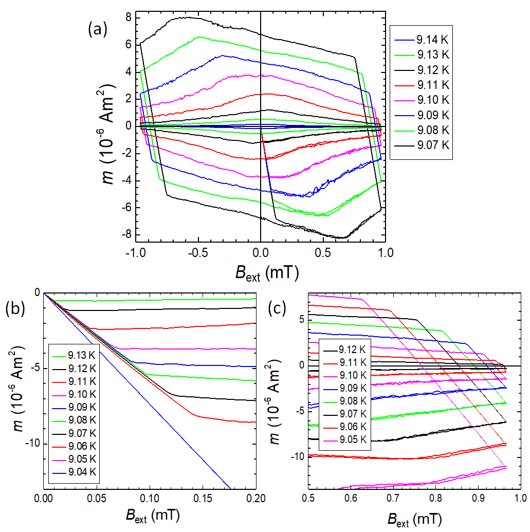
Figure 2. Magnetization loops (MHLs) measured close to Tc. (a) MHLs in the temperature range 9.07 ≤ T ≤ 9.14 K. (b). The virgin curves (VCs) of the MHLs in the temperature range 9.07 ≤ T ≤ 9.14 K. The VCs are linear and join the MHLs quite abruptly. (c). Reverse legs of the MHLs measured at 9.05 ≤ T ≤ 9.12 K. All reverse legs are linear and the ends are quite sharp, i.e., hardly rounded off.
Figure 2 (a) presents MHLs measured in Detroit on one of the Nb disk samples in the temperature range 9.07 ≤ T ≤ 9.14 K, i.e., i. e., around the characteristic temperature, Tp. Below 9.04 K (not shown here), the MHLs show the "archetypal" shape of a type-II superconductor with the shape given by the field-dependent superconducting currents induced in the sample and vortex pinning in this material. The MHLs in the transition region between 9.00 K and 9.20 K were measured with temperature steps of 0.01 K using the stationary sample technique. All the MHLs develop a more parallelogram-like shape without any low-field maximum. Note also that the slope of the virgin curve changes between 9.05 K and 9.06 K (b). There is furthermore a significant change in the shape of the reverse legs of the MHLs as shown in (c). Along with this change also the slope of the reverse leg changes to being steeper at temperatures below 9.05 K.
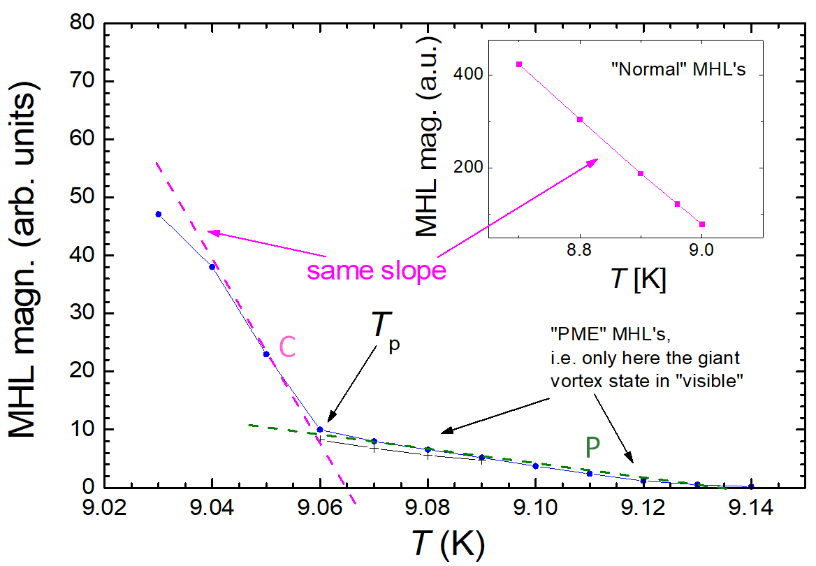
Figure 3. Evaluated details of the hysteresis measurements. The graph gives the MHL magnitude (maximum induced magnetic moment) as a function of temperature. The blue datapoints give the data obtained from the MHLs, the black crosses (+) represent the data from a second run. The slope from the archtypal MHLs as shown in the inset and the slope of the component C in the main panel are the same. It is obvious from this graph that at Tp an abrupt change in the MHL shape takes place, and the normal flux pinning vanishes. At T > 9.06 K, the component P is measured follwing a completely different slope.
Figure 3 shows the temperature dependence of the magnitude of MHL (i.e., the maximum induced magnetic moment, mmax(T). mmax(T) is nearly linear below the temperature Tp going sharply towards zero at about 9.065 K, as indicated by the magenta dashed line . The inset to Fig. 4 presents the same analysis for the temperature range 8.7 ≤ T ≤ 9.0 K, i.e., the range where the "normal" MHL shape is found. The slope obtained here and the slope of the magenta dashed line in the main panel are the same. However, above 9.06 K, mmax(T) abruptly changes the slope and decreases, again nearly linearly, but with a slope being about one order of magnitude smaller, as indicated by the dashed green line. Thus, in the temperature range Tp ≤ Tc, the PME-MHLs are visible, giving an indication of the giant vortex state.
It is obvious from this graph that the mmax(T)-dependence can be formally separated into two components, one (we will call this component "C") that goes sharply to zero at T = 9.06 K ~ Tp, and another component (we will call this component "P") that has a much weaker temperature dependence. The component P is not "visible" at temperatures below Tp, where the P component is overwhelmed by the larger C component and the magnetic moment is given primarily by the dominant component C, which describes the classic situation of flux pinning of Abrikosov vortices. The situation changes below the characteristic temperature, Tp, where the magnetic moment from the component C is (practically) zero and the mmax(T)-dependence is entierly given by the component P that diminishes only at temperatures close to T1 or higher. Considering both the shape and character of MHLs at various temperatures, and also the FC and ZFC curves studied in detail in [25], we can attribute the component C to the conventional behavior of a type-II superconductor, where induced currents are governed primarily by vortex pinning. The origin of the component P is still not fully understood. This component is obvious only above Tp, where the C component diminishes to zero, but the character of the mmax(T)-dependence indicates that the P component is present in the sample also at temperatures below Tp. We thus believe that the component P of the induced magnetic moment is responsible for specific superconducting behavior of Nb below the transition temperature including (but not limited to) the appearance of that positive magnetic moment when the sample is cooled in small applied magnetic fields (i.e., the Paramagnetic Meissner effect).
2. Appearance of the PME
Several theoretical approaches to explain the PME were already reviewed by Li [26] but only a short summary of the experimental data were given in this article. Here, it is important to point out that two basically different explanations for the PME exist in the literature:
- Extrinsic PME. Here, the PME is not related to the material properties, but to properties of the sample surface, surface superconductivity, or the spatial variation of the superconducting properties in a given sample. This is the case for the giant vortex state [27,28], flux trapping and compression effects [29], which will be discussed in detail later on in this review.
- Intrinsic PME. In this case, the PME is an inherent material property. The PME may be originating by the presence of Josephson coupled π-junctions, which could arise due to the unconventional order parameter (e.g., the d-wave symmetry in HTSc cuprates, [30,31]). Furthermore, s-wave odd-frequency superconductivity may occur in a two-band superconductor (e.g., MgB2, pnictides) or in superconductor/nonsuperconductor and superconductor-magnet hybrid systems, where the time-reversal symmetry of the superconducting condensate is broken by magnetic ordering and thus can result in the stabilization of an odd-frequency superconducting state [32].
The theoretically-oriented review of Li [26] could not provide a solution to the (still) ongoing discussion which explanation may be the correct one, leaving this question open to new results appearing in the future. Thus, it is also not the intention of the present review to revive the discussion which explanation is the correct one. Very recently, PME was also observed in superconducting boron-doped diamond thin films [33], which represents an elemental superconductor, but not a classic metallic one. Furthermore, renewed interest in superconductor/nonsuperconductor and superconductor/ferromagnetic Josephson junctions as well as in multiband superconductors led to new theoretical predictions of paramagnetic Meissner currents (intrinsic PME) in such systems [34,35]. However, the experimental proof of these predictions turned out to be difficult with currently only one successful demonstration in the literature [36].
Figure 4 presents experiments performed on a bulk Nb-disk performed in Detroit to show the extrinsic character of this PME. The red curves give the measurements on an as-prepared Nb disk, while the blue curves show what happens when abrading the sample surface. Besides the smaller magnetic signal (the sample volume was reduced by about 10%), all the characteristic features of the PME are gone when the sample surface is altered.
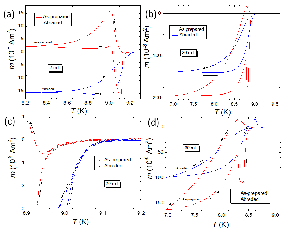
Figure 4. Abrading the surface of the Nb disks, demonstrating the extrinsic character of the PME. Two samples punched from the same Nb sheet were studied, Nb1 was left in as-prepared condition, and Nb2 was mechanically abraded on both top and bottom surface (the sample amount was reduced by 10 %). (a). FCC and FCW curves in an applied field of 2 mT. Sample Nb1 (as-prepared, red) and sample Nb2 (abraded, blue ). (b). Details around Tc of the data shown in (a). (c). FCC and FCW curves in an applied field of 20 mT. (d). FCC and FCW curves in an applied field of 60 mT. The abraded sample does not show any feature of the PME at any temperature/field as compared to the as-prepared sample Nb1.
Therefore, the present review mainly focuses on the experimental observations of the PME in metallic, s-wave superconductors in bulk or mesoscopic forms. We further provide new experimental results obtained since the first review article published in 2003, work out the distinct differences between the PME of HTSc superconductors and the metallic ones, and discuss the experimental difficulties for the observation of the PME.
The intense measurements performed on bulk Nb disks, starting from the work performed in Detroit, enabled to work out the properties of the m(T)-curves and the corresponding MHLs. From all this information, a phase diagram could be constructed (see Fig. 5 (a) and (b)). The specific shape of the MHLs found above T1 (see Figs. 2) is due to surface superconductivity, where no “classic” flux pinning prevails. Below the temperature Tp, the classic flux pinning sets in.
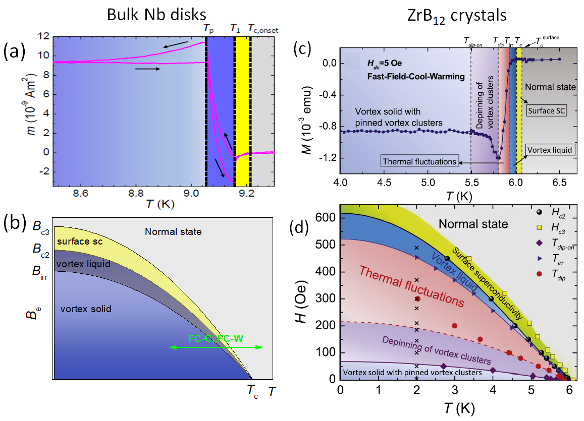
Figure 5. (a) DC m(T) measurement on a bulk Nb disk down to 8.2 K (applied field of 5 mT (5 Oe)). Note here the lower peak on the up-run being at a much higher temperature as compared to the peak measured on the down-run. (b) Schematic phase diagram constructed from the m(T) and m(H)-measurements on the Nb disks. (c) Temperature dependence of the magnetization in the fast field-cool warming (FFCW) mode at 0.5 mT (5 Oe) on ZrB12 crystals [37]. (d). Phase diagram for the PME in FFCW mode. The third critical field Hc3 is defined from the onset of the diffraction paramagnetic effect (DPE) seen as a peak in the in-phase ac susceptibility measurements; Hc2 is defined from the intersection of two linear fits of the m(T) curves above and below the onset; Tirr is derived as the onset of a diamagnetic signal on the in-phase AC susceptibility curve. The solid and dashed lines are plots of the empirical formula H(T) = H0 [1- (T/Tc)2]n. The black crosses show the field locations where magnetic relaxation curves are measured (not shown here, Fig. 6 of [37]). Images (c) and (d) reproduced with permission from [37].
Figures 5 (c) and (d) present results from Ge et al. [37] measuring ZrB12 crystals, which are unique due to non-monotonic vortex-vortex interactions. Also for this material, DC and AC susceptibility was measured as well as magnetic relaxation. From all these measurements, the parameters for the phase diagram could be determined.
3. Conclusions and Outlook
To conclude, in our recent review article we presented an overview on the experimental data of PME observed on various metallic samples using either magnetometry, AC susceptibility or various magnetic imaging techniques. Several different materials were found in the literature to exhibit the PME, and several different shapes of samples were involved: single crystals, polycrystalline bulks, nanowires and nanowire arrays, thin films, mesoscopic samples patterned from thin films, multilayers and bulk wires (in the case of MgB2) were studied. Among them, the bulk Nb disks, the Al and Nb mesoscopic films [38] and the ZrB12 crystals were analyzed in detail to refine the flux compression and giant vortex state models. Thus, there are now well-defined theoretical explanations for most features of PME, which are valid for many different types of superconducting samples. The models of flux compression and the giant vortex state may, as already detailed by Geim et al. [38] be valid even for the polycrystalline HTSc samples. However, not all features of the PME are fully understood, and hence, there is still room for more detailed measurements to further elucidate those only partially understood observations found in the literature. With the development of new imaging techniques like photoresponse imaging [39], new insights to the origin of PME may become possible.
The more recently discussed odd s-wave superconductivity in multilayer samples may bring up a paramagnetic Meissner effect and this was also proven experimentally [36]. This new tunability of the Meissner effect offers an unique way to design superconductor/ferromagnet structures for superconducting spintronics [42].
Future work on PME will consider very thin films of metallic superconductors, where significant progress has been made to fabricate uniform atomic monolayer films of Pb, Nb, Al, V and MgB2. Giant PME may appear from non-monotonic vortex interactions as predicted in [40]. In addition, the fabrication of new superconducting polymorphs by nanostructuring may open new ways to induce PME [41], and superconducting spintronics [42] may make use of the PME and develop new application possibilities. These all present interesting possibilities for PME in future work!
This entry is adapted from 10.3390/met13061140
References
- Onnes, H.K. Part I.-- Laboratory methods of liquefaction. On the lowest temperature yet obtained. Trans. Faraday Soc. 1922, 18, 145-174.
- Meissner, W.; Ochsenfeld, R. Ein neuer Effekt bei Eintritt der Supraleitfähigkeit. Naturwissenschaften 1933, 21, 787-788, doi: 10.1007/BF01504252.
- Tinkham, M. Introduction to Superconductivity, 2nd ed.; Dover Publications Inc.: New York, USA, 1996.
- Savitskii, E. M.; Baron, V. V.; Efimov, Yu. V.; Bychkova, M. I.; Myzenkova, L. F. Superconducting Materials, 1st ed.; Plenum Press: New York, London, 1973.
- Rose-Innes, A.C.; Rhoderick, E.H. Introduction to Superconductivity, 2nd ed.; Pergamon Press plc.: Oxford, U.K., 1978.
- Buckel, W.; Kleiner, R. Supraleitung. Grundlagen und Anwendungen, 7th ed.; Wiley-VCH: Weinheim, Germany, 2013; doi: 10.1002/9783527668670.
- Narlikar, A.V. Superconductors, Oxford University Press, U.K., 2014.
- Koblischka, M. R. Magnetic properties of high-temperature superconductors, Alpha Science International Ltd.: Oxford, U.K., 2009.
- Pitaevskii, L. Phenomenology and Microscopic Theory: Theoretical Foundations. In: Superconductivity. Conventional and Unconventional Superconductors, Vol. 1; Bennemann, K.H.; Ketterson, J.B., Eds.; Springer: Berlin, Heidelberg, 2008.
- Mangin, P.; Kahn, R. Superconductivity. An Introduction, Springer: Cham, Switzerland, 2017.
- Svedlindh, P.; Niskanen, K.; Norling, P.; Nordblad, P.; Lundgren, L.; Lönnberg, B.; Lundström, T. Anti-Meissner Effect in the BiSrCaCuO System. Physica C 1989, 162–164, 1365-1366; doi: 10.1016/0921-4534(89)90735-1.
- Blunt, F. J.; Perry, A. R.; Campbell, A. M.; Liu, R. S. An investigation of the appearance of positive magnetic moments on field cooling some superconductors. Physica C 1991 175, 539-544; doi: 10.1016/0921-4534(91)90262-W.
- Braunisch, W.; Knauf, N.; Kataev, V.; Neuhausen, S.; Grütz, A.; Kock, A.; Roden, B.; Khomskii, D.; Wohlleben, D. Paramagnetic Meissner Effect in Bi High-Temperature Superconductors, Phys. Rev. Lett. 1992 68, 1908-1911, doi: 10.1103/PhysRevLett.68.1908.
- Braunisch, W.; Knauf, N.; Bauer, G.; Kock, A.; Becker, A.; Freitag, B.; Grütz, A.; Kataev, V.; Neuhausen, S.; Roden, B.; Khomskii, D.; Wohlleben, D. Paramagnetic Meissner effect in high-Tc superconductors. Phys. Rev. B 1993 48, 4030-4042; doi: 10.1103/PhysRevB.48.4030.
- Khomskii, D. Wohlleben effect (Paramagnetic Meissner effect) in high-temperature superconductors. J. Low Temp. Phys. 1994 95,205-223; doi: 10.1007/BF00754937.
- Thompson, D. J.; Minhaj, M. S. M.; Wenger, L. E.; Chen, J. T. Observation of Paramagnetic Meissner Effect in Niobium Disks, Phys. Rev. Lett. 1995 75, 529-532, doi: 10.1103/PhysRevLett.75.529.
- Koblischka, M.R.; P˚ust, L.; Chikumoto, N.; Murakami, M.; Nilsson, B.; Claeson, T. Paramagnetic Meissner response of an artificially granular YBCO thin film. Physica B 2000, 284-288, 599-600; doi: 10.1016/S0921-4526(99)02226-7.
- Minhaj, M. S. M.; Thompson, D. J.; Wenger, L. E.; Chen, J. T. Paramagnetic Meissner Effect in a Niobium Disk. Physica C 1995 235-240, 2519-2520, doi: 10.1016/0921-4534(94)92480-5.
- Kostic, P.; Veal, B.; Paulikas, P.; Welp, U.; Todt, V. K.; Gu, C.; Geiser, U.; Williams, J. M.; Carlson, K. D.; Klemm, R. A.Paramagnetic Meissner effect in Nb. Phys. Rev. B 1996 53, 791-801; doi: 10.1103/PhysRevB.53.791.
- Rice, T. M.; Sigrist, M. Comment on `Paramagnetic Meissner effect in Nb'. Phys. Rev. B 1997 55, 14647-14648; doi: 10.1103/PhysRevB.55.14647.
- Kostic, P.; Veal, B.; Paulikas, P.; Welp, U.; Todt, V. K.; Gu, C.; Geiser, U.; Williams, J. M.; Carlson, K. D.; Klemm, R. A. Reply to Comment on `Paramagnetic Meissner effect in Nb'. Phys. Rev. B 1997 55, 14649-14652; doi: 10.1103/PhysRevB.55.14649.
- Fodor, P. S.; Wenger, L. E. Paramagnetic Meissner effect in Nb disks. Physica C 2000, 341-348, 2043-2044, doi: 10.1016/S0921-4534(00)00991-6.
- Thompson, D. J.; Wenger, L. E.; Chen, J. T. Inducing and enhancing the paramagnetic Meissner effect in Nb disks. Czech J. Phys. 1996, 46, 1195-1196; doi: 10.1007/BF02562712.
- Thompson, D. J.; Wenger, L. E.; Chen, J. T. Inducing the paramagnetic Meissner effect in Nb disks by surface ion implantation. Phys. Rev. B 1996 54, 16096-16100; doi: 10.1103/PhysRevB.54.16096.
- Pust, L.; Wenger, L. E.; Koblischka, M. R. Detailed investigation of the superconducting transition of niobium disks exhibiting the paramagnetic Meissner effect. Phys. Rev. B 1998, 58, 14191-14194, doi: 10.1103/PhysRevB.58.14191.
- Li, M.S. Paramagnetic Meissner effect and related dynamical phenomena. Phys. Rep. 2003 376, 133-223; doi: 10.1016/S0370-1573(02)00635-X.
- Moshchalkov, V. V.; Qiu, X. G.; Bruyndoncx, V. Paramagnetic Meissner effect from the self-consistent solution of the Ginzburg-Landau equations. Phys. Rev. B 1997 55, 11793-11801; 10.1103/PhysRevB.55.11793.
- Moshchalkov, V. V.; Qiu, X. G.; Bruyndoncx, V. The paramagnetic Meissner effect resulting from the persistence of the giant vortex state. J. Low Temp. Phys. 1996 105, 515-520; doi: 10.1007/BF00768437.
- Koshelev, A. E.; Larkin, A. I. Paramagnetic moment in field-cooled superconducting plates: Paramagnetic Meissner effect. Phys. Rev. B 1995 52, 13559-13562; doi: 10.1103/PhysRevB.52.13559.
- Chaban, I. A. Paramagnetic Meissner effect. J. Supercond. Nov. Magn. 2000 13, 1011-1017; doi: 10.1023/A:1026467825612.
- Higashitani, S. Mechanism of paramagnetic Meissner effect in high-temperature superconductors. J. Phys. Soc. Jpn. 1997 66, 2556-2559; doi: 10.1143/JPSJ.66.2556.
- Linder, J.; Balatsky, A.V. Odd-frequency superconductivity. Rev. Mod. Phys. 2019, 91, 045005; doi: 10.1103/RevModPhys.91.045005.
- Govindaraj, L.; Arumugam, S.; Thiyagarajan, R.; Kumar, D.; Kannan, M.; Das, D.; Suraj, T.S.; Sankaranarayanan, V.; Sethupathi, K.; Baskaran, G.; Sankar, R.; Rao, M.M.C.D. Wohlleben Effect and Emergent π-junctions in superconducting Boron doped Diamond thin films. Physica C 2022, 598, 1354065; doi: 10.1016/j.physc.2022.1354065.
- Mironov, S.; Mel’nikov, A.; Buzdin, A. Vanishing Meissner effect as a Hallmark of in–Plane Fulde-Ferrell-Larkin-Ovchinnikov Instability in Superconductor–Ferromagnet Layered Systems. Phys. Rev. Lett. 2012, 109, 237002; doi: 10.1103/PhysRevLett.109.237002.
- Ouassou, J.A.; Belzig,W.; Linder, J. Prediction of a Paramagnetic Meissner Effect in Voltage-Biased Superconductor–Normal-MetalBilayers. Phys. Rev. Lett. 2020, 124, 047001; doi: 10.1103/PhysRevLett.124.047001.
- Di Bernardo, A.; Salman, Z.; Wang, X.L.; Amado, M.; Egilmez, M.; Flokstra, M.G.; Suter, A.; Lee, S.L.; Zhao, J.H.; Prokscha, T.; Morenzoni, E.; Blamire, M.G.; Linder, J.; Robinson, J.W.A. Intrinsic Paramagnetic Meissner Effect Due to s-Wave Odd-Frequency Superconductivity. Phys. Rev. X 2015, 5, 041021; doi: 10.1103/PhysRevX.5.041021.
- Ge, J.Y.; Gladilin, V.N.; Sluchanko, N.E.; Lyashenko, A.; Filipov, V.B.; Indekeu, J.O.; Moshchalkov, V.V. Paramagnetic Meissner effect in ZrB12 single crystal with non-monotonic vortex-vortex interactions. New. J. Phys. 2017, 19, 093020; doi: 10.1088/1367-2630/aa8246.
- Geim, A.K.; Dubonos, S.V.; Lok, J.G.S.; Grigorieva, I.V.; Maan, J.C.; Theil Hansen, L.; Lindelof, P.E. Ballistic Hall micromagnetometry. Appl. Phys. Lett. 1997, 71, 2379-2381; doi: 10.1063/1.120034.
- Zhuravel, A. P.; Bae, S.; Shevchenko, S. N.; Omelyanchouk, A. N.; Lukashenko, A. V.; Ustinov, A. V.; Anlage, S. M. Imaging the paramagnetic nonlinear Meissner effect in nodal gap superconductors. Phys. Rev. B 2018, 97, 054504; doi: 10.1103/PhysRevB.97.054504.
- da Silva, R.M.; Milosevic, M.V.; Shanenko, A.A.; Peeters, F.M.; Aguiar, J.A. Giant paramagnetic Meissner effect in multiband superconductors. Sci. Rep. 2015, 5, 12695; doi: 10.1038/srep12695.
- Koblischka, M.R.; Koblischka-Veneva, A. Superconductivity 2022. Metals 2022, 12, 568; doi: 10.3390/met12040568.
- Linder, J.; Robinson, J. W. A. Superconducting Spintronics. Nature Phys. 2015, 11, 307; doi: 10.1038/nphys3242.
This entry is adapted from the peer-reviewed paper 10.3390/met13061140
