You're using an outdated browser. Please upgrade to a modern browser for the best experience.
Green Substrates for Flexible Electronics for IoT: History
Please note this is an old version of this entry, which may differ significantly from the current revision.

The Internet of Things (IoT) is gaining more and more popularity and it is establishing itself in all areas, from industry to everyday life. Given its pervasiveness and considering the problems that afflict today’s world, that must be carefully monitored and addressed to guarantee a future for the new generations, the sustainability of technological solutions must be a focal point in the activities of researchers in the field. Many of these solutions are based on flexible, printed or wearable electronics. The choice of materials therefore becomes fundamental, just as it is crucial to provide the necessary power supply in a green way.

  • flexible electronics
  • IoT
  • substrates
  • nanopaper
  • sustainability

1. Introduction

The term sustainability has now become commonly used, it is of great importance and is also used in different contexts. It was used for the first time in 1992, during the first UN Conference on the environment. The definition of sustainability that has been given is this: Condition of a development model capable of ensuring the satisfaction of the needs of the present generation without compromising the possibility of future generations to realize their own [1]. This definition is centered not only on the economy and society, but above all on ecology. Sustainability and sustainable development are linked to a new idea of well-being that takes into account people’s quality of life. Environmental sustainability requires responsibility in the use of resources. It is therefore a development model to which everyone can and must contribute, starting from the awareness that every action performed by each of us has a deep impact on the environment.
Based on these considerations, the world of electronics, which for decades has been increasingly pervasive in all sectors of life (industry, medical, automation, automotive, military, consumption), cannot fail to pay maximum attention to the issue of sustainability. The electronics as fuel of the Internet of Things technology is surely leading us in a new way of conducting our lives and cities [2], also allowing the optimization of the production processes of companies and industries and the management of services and infrastructures, limiting the consumption of resources and pollution. Management of public lighting [3,4,5,6,7], air quality [8,9,10,11,12,13,14,15,16,17,18,19,20,21,22] and noise pollution monitoring [23,24,25,26,27,28,29], smart home [30,31,32,33,34,35,36,37,38,39,40,41,42,43], smart roads, smart cars, urban mobility and transport [44,45,46,47,48,49,50,51,52,53,54,55,56,57,58,59,60,61,62,63], food and agriculture [64,65,66,67,68,69,70,71,72,73,74,75,76,77,78,79,80,81,82,83], smart factories [84,85,86,87,88,89,90,91] and medicine [92,93,94,95,96,97,98,99,100,101,102] are examples of the great potentialities of the IoT. However, the increase in connectivity inevitably translates into an increase in electronic devices and systems (sensors, data acquisition and processing systems, communication systems) and therefore the problem of respecting the environment, both in the production step and disposal of disused systems is, nowadays, of fundamental importance also in the field of the IoT industry. Thanks to the availability of eco-compatible materials, flexible electronics, which is a solution that is increasingly gaining space in many applications due to its portability, wearability and low cost, could be the right path towards an increasingly green IoT (
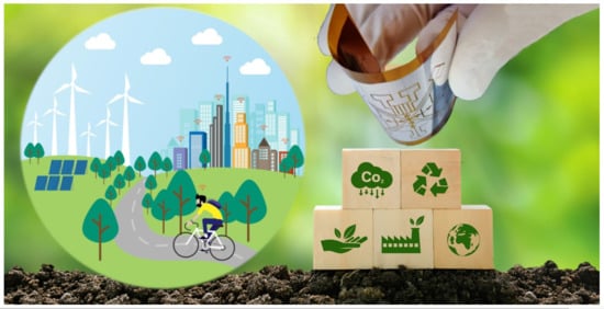
Figure 1).
Figure 1. Flexible electronics is an important building block for the creation of a sustainable and interconnected world.

2. Green Substrates: Paper and “Nanopaper”

The choice of the substrate on which to make a flexible device is surely a key factor for sustainable IoT because the greater quantity of material that makes up the device is precisely the substrate [105].
With the advent of flexible electronics, the favored substrates on which to build devices have, for a long time, been plastic materials. However, discarded plastics degrade to form micro and nano-plastics that are hazardous to human beings and the environment. If one thinks of the implementation of flexible devices that are “green”, surely paper is the first material that comes to mind as a substrate to substitute plastic [106]. In fact, paper is widely and easily available, low-cost, recyclable and biodegradable. Table 1 shows a comparison between paper and the plastic materials mostly used as substrates, in terms of impacts on climate change and resource use [107]. In this regard, it may be useful to recall that studies conducted on these same indicators as regards the production of silicon, the fundamental semiconductor in the electronics industry, have highlighted a development in the wrong direction for the silicon industry, facing increasing climate related pressures [108].
Table 1. Comparison between paper and the most used plastic substrates, in terms of the impact on climate change and resource use.
Substrate Material Climate Change Impact
kg CO2 eq. */Sheet ***
Resource Use
kg Sb eq. **/Sheet ***
Paper 1.3 × 10⁻⁴ 5.2 × 10⁻¹¹
PET (polyethylene terephthalate) 1.5 × 10⁻³ 1.8 × 10⁻¹⁰
PEI (polyetherimide) 1.3 × 10⁻² 2.0 × 10⁻⁹
PEEK (polyether ether ketone) 7.4 × 10⁻³ 2.2 × 10⁻⁹
* Indicator of potential global warming due to emissions of greenhouse gases to the air. ** Indicator of the depletion of natural non-fossil resources. *** Sheet with 25 cm2 surface area, 125 mm thickness.
Although it is very promising from an environmental point of view and several devices made on paper substrates have appeared in the last decade, the use of paper as a substrate is still limited, due to the high surface roughness and poor barrier properties against water and solvents [106]. However, if we consider that in applications in the IoT field, and therefore in electronics, one of the main properties of the substrates is that of allowing optimization of the device performance in terms of conductivity, paper substrates have performances no lower than the plastic ones most used up to now. In [106] an interesting comparison is made between different paper substrates and PET substrates. The main results are summarized in Table 2.
Table 2. Comparison between conductivity of the printed layer on paper and PET substrates. The layer thickness used in the volume resistivity measurement was considered to be equal on every substrate. An ink transfer volume of 7 mL/m2 has been considered.
Printing Technique Substrate Material Sheet Resistance
mΩ/Square
Volume
Resistivity (Ω·cm)
Flexo-printing P1 * 177 ± 19 2.2 × 10⁻⁶
P2 ** 169 ± 16 1.6 × 10⁻⁶
PET *** 260 ± 23 2.1 × 10⁻⁶
Rotary
screen-printing
P1 45.3 ± 1.3 4.1 × 10⁻⁵
P2 39.4 ± 0.6 3.4 × 10⁻⁵
PET 52.3 ± 2.5 4.7 × 10⁻⁵
* Coated paper, Stora Enso NovaPress Silk, 80 g/m2. ** Coated paper, ultra-smooth top side for printed electronics, Arjo Wiggins PowerCoat HD, 95 g/m2. *** Melinex ST506 (DuPont Teijin Films, Chester, VA, USA).
Continuing with the comparison between paper and plastic substrates, wishing to evaluate the performances in terms of elasticity, in Table 3 we report Young’s modulus. Among the plastic materials we have considered PET, precisely because it is the most used, PEN (polyethylene naphthalate) which has performances in terms of elasticity superior to other plastic substrates, and PDMS (polydimethylsiloxane), a popular elastomer in the manufacture of stretchable devices [109]. Results in Table 3 show that paper substrates can offer elastic performances comparable to PDMS under proper coating conditions.
Table 3. Comparison of Young’s modulus of paper and plastic substrates [109].
Substrate Material Young’s Modulus [GPa]
Paper Up to 3.5 *
PET 2.8
PEN 3.0
PDMS Up to 3.7 **
* Depending on coating. ** Depending on different crosslinking density.
Obviously, if the goal of making flexible devices that are absolutely sustainable is to be achieved, the separation of electronic materials, conductive metallic inks in most cases, from the paper substrate at the end of life of the devices must be easily performed. To overcome these limitations, a few solutions based on coating approaches have been presented to improve paper substrate performances. As an example, the use of shellac, that is a cheap biopolymer, has been proposed in [110]. Shellac, employed as a coating surface for paper substrates, forms planarized, printable surfaces. At the end of the life of the device, shellac behaves as a sacrificial layer that can be removed by immersing the printed device in methanol, enabling the separation of the paper substrate. Nevertheless, coating procedures and other surface treatments are not effective for all electronics applications [111,112]. In the last period, “nanopaper”, that is, planar substrates made of cellulose nanomaterials (CNM), gained relevance [113,114,115,116,117,118,119,120]. CNM are nanosized particles with highly ordered cellulose chains aligned along the bundle axis, that exhibit interesting characteristics with respect to pulp fibers and wood particles, such as high mechanical properties, low thermal expansion, low density, and simplicity of treatment that allows the implementation of additional functionalities [121,122,123]. To focus on sustainability, it is also important to evaluate the end-of-life performance, that is to carry out a study on the biodegradability of materials. In [114], for example, a comparison between the biodegradation of CNM samples with respect to microcrystalline cellulose (MCC), and a commercial thermoplastic polyurethane (TPU) has been performed and the results are summarized in Table 4.
Table 4. Example of biodegradability test on cellulose based and plastic samples. The test duration was 127 days [114].
Sample * Status Biodegradation **
CNF 50%, HEC 50% Printed 74%
CNF 50%, HEC 50% Unprinted 78%
MCC Unprinted 94%
TPU Unprinted No degradation
* CNF: cellulose nanofibrils; HEC: hydroxyethyl cellulose; MCC: microcrystalline cellulose; TPU: thermoplastic polyurethane. ** The data are extrapolated from [114]. Biodegradation of samples was estimated firstly by employing the CO2 evolution method and, secondly, by visually evaluating samples disintegration in soil upon burial.
The results reported in [114] show that in the first 70 days of testing, the biodegradability rate of the CNF-HEC compounds is comparable to that of pure cellulose, while subsequently there is a slowdown. Although there is no doubt that the biodegradability of cellulose-based samples is far superior to that of plastic materials, it is certainly clear that, to further improve the state of the art, studies need to be conducted to understand how to optimize the performance of paper substrates without lowering the biodegradability performance too much compared to pure cellulose. The biodegradability of the printed substrate is slightly lower than that of the non-printed substrate, also highlighting the importance of working on the eco-sustainability of the conductive layers. Without any doubt, the “nanopaper” technology, that is a relatively low-cost technology [124,125,126] for substrate fabrication for IoT applications, is strategic to fuel a transition toward a sustainable and green IoT, also working on the use of optimized nanocellulose with other materials and hybrid structures [127,128,129,130,131].

This entry is adapted from the peer-reviewed paper 10.3390/s23115264

This entry is offline, you can click here to edit this entry!
Academic Video Service