The combination of integrated optics technologies with nonlinear photonics, which has led to the growth of nonlinear integrated photonics, has also opened the way to groundbreaking new devices and applications. They have been made possible by the design of guided-wave structures, which can enhance the material’s nonlinear properties, and/or by the availability of suitable materials, with high nonlinear coefficients.
Here, first, various waveguide structures are presented, then the fabrication processes and integration platforms, referring to most common utilized materials, semiconductors, glasses and lithium niobate are discussed. Finally, some examples of nonlinear photonic integrated devices to be employed in optical communications, all-optical signal processing and computing, or in quantum optics are reported.
- photonics devices
- nonlinear photonics
- integrated photonics
- photonic structures
- optical materials
- all-optical signal processing
- all-optical computing
- all-optical communications
- all-optical digital devices
- nonlinear optical sources
1. Introduction
In 1969, inspired by the rapid development of integrated electronics, the concept of integrated optical circuits (IOCs) was proposed by researchers at Bell Labs [1]. Some ten years later, the growth in complexity of the optical architectures led to the introduction of the term photonic integrated circuits (PICs), and in 1991 a paper, again by researchers at AT&T Bell Labs, presented an early review of InP-based PICs [2]. Then, it took more than a decade to have the announcement of a breakthrough in photonic integration with the industry’s first large-scale PIC: a 2005 article described a 100-Gb/s dense wavelength division multiplexed (DWDM) transmitter and receiver PIC, fabricated through the integration of over 50 discrete functions onto a single monolithic InP chip [3].
Integrated optic and photonic chips have huge potential for low-cost, scalable production, and high-density components integration [4][5][4, 5]. Photonic building blocks can be passive (e.g., couplers, switches, modulators, multiplexers) or active (e.g., amplifiers, detectors, and lasers). The first nonlinear optics experiment in waveguides, showing second harmonic generation (SHG) in GaAs waveguides, was reported in 1971 [6]. Since the efficiency of nonlinear interaction depends upon the interacting beam intensities (power/area) and it is also proportional (either linearly or quadratically) to the interaction distance, it became soon clear that optical waveguides offer important advantages. Firstly, the confinement of light intensity within an area comparable to the wavelength of light leads to an enhanced field-strength and high power density; secondly, the diffractionless propagation in one or two dimensions results in interaction lengths over a distance (at least of the order of centimeters, if not longer) much longer than the one obtained within a bulk material. Despite the difficulties, thanks to the development of novel light sources, advanced materials and very effective guiding structures [7][8][9][10][11][12][7-12], impressive progress has been made in nonlinear integrated optics (NLIO) and, more broadly, in nonlinear integrated photonics (NLIP), paving the way to a full integration of complete optical information transmission and processing systems in a monolithic or hybrid chip. The evolving nano-devices would enable advanced applications not only in optical processing and computing, but also in metrology, single-molecule sensing, imaging, microscopy, mid-infrared photonics, terahertz generation, microwave photonics and bio-medicine [12].
2. Integrated photonic structures
Guided wave structures, resulting from the coupling between an electromagnetic field and some kind of resonance, are the basic blocks for photonics integrated circuits.
2.1 Optical 2D and 3D waveguides
The resonance can be geometric, as it occurs in thin-film optical waveguides where constructive interferences result in guiding light, due to total internal reflection. Thus, integrated optical waveguides can be classified depending on geometry. Planar (2D) dielectric waveguides are constituted by layers of high and low refractive index materials providing confinement only in vertical direction. Nonplanar (3D) waveguides, providing confinement in two directions, can have different cross sections, such as ridge, rib, stripe-loaded, or buried; slot structures, moreover, can have different forms of guiding core surrounded by cladding material (see Fig. 1 for some examples) [13]. Correspondingly, the most suitable fabrication methods must be selected (e.g., high- or low-energy diffusion, thin-film deposition, direct laser writing). The need of efficient coupling to other integrated components makes the channel waveguide the most commonly used structure.
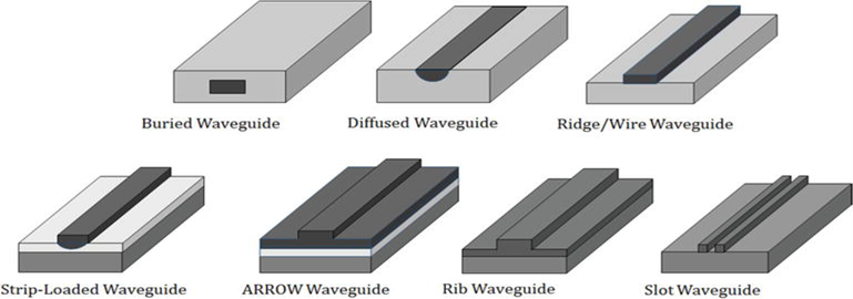
Figure 1.
Schematic representation of various channel waveguides. Adapted from [13] under Creative Commons License 3.0.
2.2 Microresonators and photonic crystals
During the last decades, the fast growth of micro-scale fabrication techniques has enabled the successful demonstration of various types of microphotonic devices. The key challenges were a reduction in the size of optical devices and an improvement of their performances. The main goal was to go beyond the limit of integrated optics, offering a reliable platform for dense integration [14].
Special attention has been addressed to microcavities [15] and photonic crystals (PhCs) [16], which combine a small modal volume with very high optical quality factor (Q). In these microphotonics devices, due to their reduced size, photons are trapped in small volumes close to the diffraction limit for sufficiently long times, so that these photons strongly interact with the host material, creating enhanced nonlinear effect and a significant reduction of their power threshold.
WGMRs have shown high mode stability and ultra-high-quality factors Q, up to 1011. These resonators are excellent platforms for fundamental and applied studies of nonlinear processes, due to their long photon lifetime (temporal confinement) and their small mode volume (spatial confinement) [17][18][19][20][17-20]. Temporal and spatial confinement have made possible optical frequency conversion with low-power continuous wave (CW) lasers with powers ranging from micro-watts to milliwatts [21]. Figure 2 shows different types of optical microcavities. It must be underlined that, even if more difficult to integrate in a compact structure, microspherical resonators play an important role in nonlinear photonics [22].
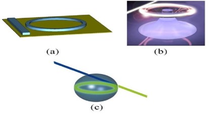
Figure 2. Different types of optical microcavities: (a) Micro-ring resonator, (b) Micro-toroid resonator, (c) Micro-sphere resonator. Adapted from [22] under Creative Commons License 3.0.
Photonic crystals provide an excellent building block for photonic integrated circuits and for enhancing a variety of nonlinear optical processes, too [23][24][25][26][23-26]. A strong advantage of PhCs cavities with ultra-small mode volume Vm is that quality factors can be relaxed while still achieving excellent Q/Vm values; despite the fact that the quality factor is inversely proportional to the linewidth of the cavity, both high-bandwidth and low-threshold all-optical processes can be realized in a single system. Integration issues, of course, must be considered in the case of PhCs, too, especially for 3D structures [25].
Figure 3 shows the design of a dispersion-engineered slow-light photonic crystal waveguide (PhCW); the blue circles represent the air-holes in a standard single-line defect (W1) PhCW with a lattice constant a, while the red circles represent the engineered air-holes, with radius decreasing from R to R2 and horizontally shifted from the dashed circles by ΔX [26].
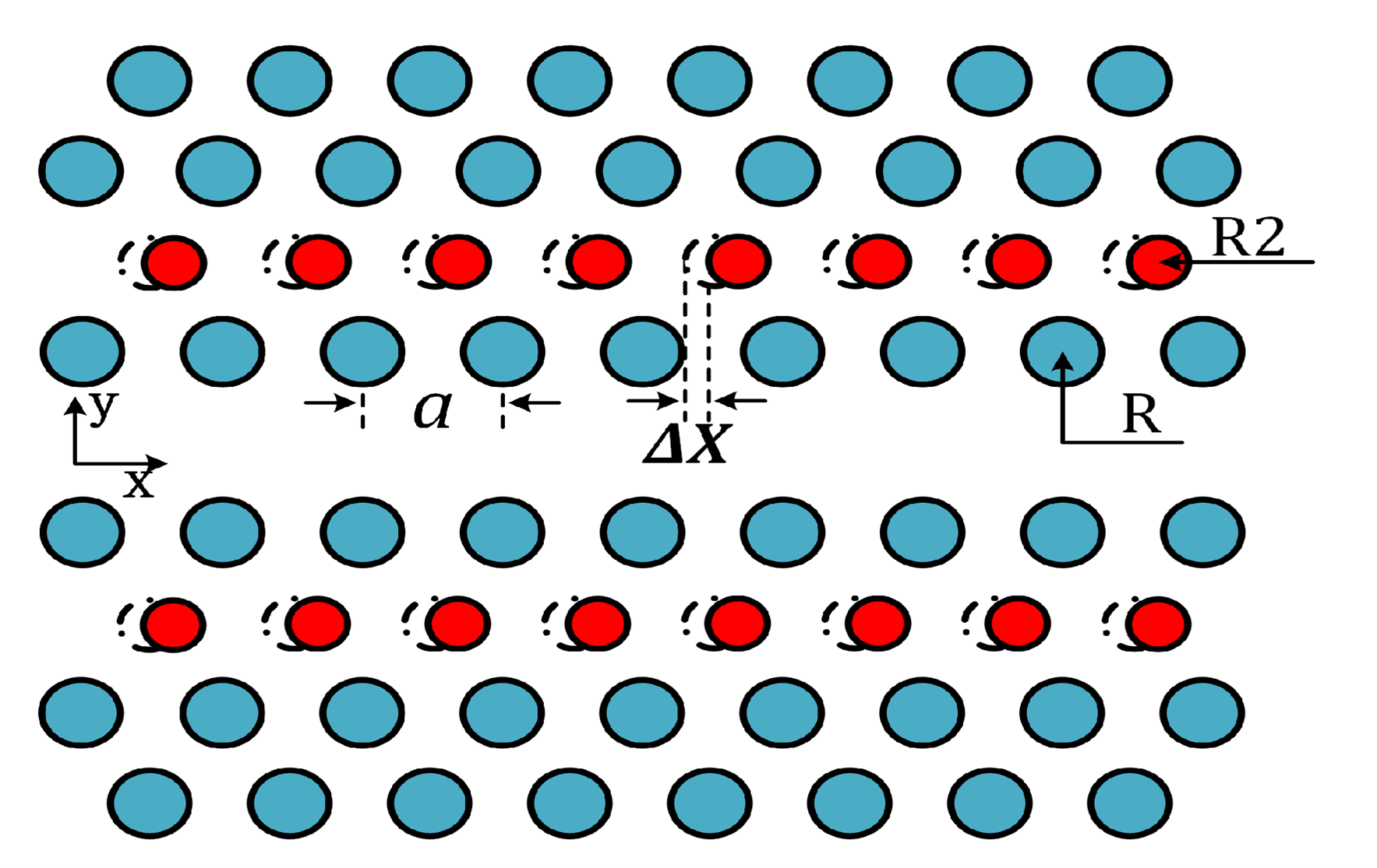
Figure 3. Structure of a photonic crystal waveguide, with air holes represented by blue and red circles. Simulations were made by considering standard silicon-on-insulator air-bridge PhCW of 220 nm thickness, lattice period 400 nm and radius R of the first air-holes row 100 nm. By adjusting the radius R2 and lattice positions ΔX of the second air-holes rows, a very wide flat band larger than 50 nm could be obtained. Reproduced from [26] under Creative Commons License 3.0.
Guided waves can also result from a coupling between an electromagnetic field and a resonance related to material properties. For example, the plasma resonance associated with the electron gas in a metal can be coupled to an electromagnetic field via the interaction between the field and the charges, leading to surface plasmon. These surface waves, propagating along the dielectric–conductor interface, are evanescently confined in the perpendicular direction due to very shallow penetration of the electromagnetic field into the metal. Plasmonic waveguiding allows breaking the diffraction limit of light, opening possibilities for subwavelength light confinement. To increase integration density and compactness of photonic structures, many different geometries of plasmonic waveguide have been investigated in recent years, including interferometers and ring resonators [27] and periodic metal structures [28]. However, in all cases, energy dissipation in closely spaced metal layers causes high losses, limiting the propagation length to a few micrometers.
2.3 Nanophotonics structures
Electromagnetic metamaterials are artificial media in which subwavelength electromagnetic constituents replace atoms as the basic structural elements to control the light–matter interaction. Many of novel phenomena related to metamaterials are due to optical magnetism, observed in specifically designed artificial subwavelength structures, even when such structures are made of non-magnetic materials. The most popular constitutive elements of metamaterials are made of metals, where free electrons oscillate back and forth, creating effective loops of current, thus inducing an efficient magnetic response. Plasmonic nanostructures support field localization due to localized surface-plasmon resonances with multipolar electric-type characteristics. The plasmonic resonances, generally, result in high field enhancement, but at the price of higher absorption losses due to free-carrier absorption and reduced optical damage thresholds [29].
In order to control light–matter interactions at the nanoscale, the most disruptive strategy would be to replace metals by all-dielectric nanoparticles with high refractive index [30][31][32][30-32], providing fine control over the light features (amplitude, phase and polarization). Dielectric nanoparticles support an alternative mechanism of light localization in subwavelength optical structures via low-order dipole and multipole Mie resonances [33]. They may generate magnetic response via the displacement current contribution, playing a crucial role in the realization of the unique functionalities of meta-atoms, also driving novel effects in the fields of metamaterials and nanophotonics. Figure 4 presents a schematic illustration of some metastructures [34].
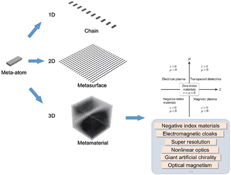
Figure 4. Schematic illustration of meta‐atom, 1D chain, 2D metasurface, and 3D metamaterial. Inserts are the representation of the parameter space for permittivity ε and permeability μ and the typical examples of applications of metamaterials. Adapted from [34] under Creative Commons License 3.0.
There is a strong interest in exploring interesting physical mechanisms to create the optical resonances in such structures, for example using guided-mode resonances [35] and bound-states in continuum resonances [36], to enhance local electric fields and consequently amplify the nonlinear optical effects in metamaterials [37][38][39][40][41][37-41]. Bound states in the continuum (BIC) are special wave solutions embedded in a radiative continuum, which, however, remain localized without coupling to the extended waves or radiation [42][43][42, 43].
3. Material platforms for nonlinear integrated photonics
Numerous materials for integrated nonlinear optics have been investigated: among them, Si and related materials, such as SiN, amorphous silicon (a-Si), and SiC; glasses, such as silica, high-index glass, and chalcogenide glasses; III–V semiconductors, in particular AlGaAs; ferroelectrics, in particular lithium niobate (LN). Other recently investigated materials are tantalum pentoxide (Ta2O5) and vanadium dioxide (VO2) [[44]44 and references therein]. Correspondingly, several material platforms have been developed to achieve the goal of a dense components’ integration. Each platform has its advantages and disadvantages and offers variable nonlinear efficiencies and integration densities depending on the values of the nonlinear coefficients and refractive index contrast. An additional limiting factor is related to losses that are determined by both the quality of the grown material and the maturity of the fabrication processes, which affect, for instance, the roughness and absorption of the surface passivation layer. Although in the longer term the growth and fabrication quality for all these materials will eventually level up, there still remains one important limiting factor that clearly separates them regarding high power densities, namely two photon absorption (TPA). TPA is determined by the band gap of the material and by the working wavelength, which is often in the telecom range due to the historically developed infrastructure of sources, detectors, etc. In this regard, small-band-gap semiconductors, such as Si [45][46][47][48][49][45-49] and GaAs [50, [50][51]51], are fundamentally limited and there seems to be no way around this problem other than to change the working wavelength and all the surrounding infra-structure.
Silicon photonics research and development has much progressed, and both component performance and integration complexity have made significant steps forward in the past decade [45][46][47][48][49][45-49]. Nowadays, silicon-based platforms, in particular silicon-on-insulator (SOI), are among the most mature for PIC realization. In the SOI platform, the functional optical elements are situated in the thin top silicon layer, and the insulator is typically made of SiO2. The SOI platform has become the foundation of silicon photonics for several reasons, including strong optical confinement of silicon due to the significant refractive index difference between silicon and SiO2, which enables very compact optical devices with low optical propagation loss, high process yield, low cost, etc.
Among the numerous nonlinear waveguide platforms that have been explored, the group of materials capable of combining both passive waveguides, for light steering and nonlinear manipulation, and active functionalities (laser sources, modulators, and detectors) monolithically on the same chip is that of III–V semiconductors [50][51][50, 51]. This has been a strong driving force, stimulating development of nonlinear optical devices based on III–V semiconductors and addressing challenges associated with loss mitigation and nonlinearity enhancement in these platforms. The main III–V integrated nonlinear photonic platforms considered to date are GaAs [50][51][50, 51] and its AlGaAs derivative [52], InP and InGaAsP, III-nitrides AlN [53], and GaN [54], as well as GaP [55] and its ternary derivative InGaP. We note that AlN [53] shows optical properties similar to SiN (refractive index, transparency, and n2) but also possesses second-order nonlinearity.
Considering AlGaAs, the structures used in NLIP can be divided into three-layer, two-layer, and multi-layer platforms depending on the number of epitaxially grown layers with different material compositions. Figure 5 shows examples of these three AlGaAs platforms; the waveguides sketched in Figure 5h,i are often employed for phase matching of the χ(2) processes.
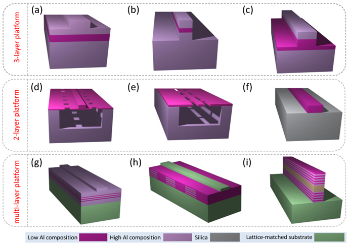
Figure 5. Schematics of AlGaAs platforms and waveguide geometries. (a–c) 3-layer platform with strip-loaded, nanowire, and half-core waveguides, respectively. (d–f) 2-layer platforms with suspended nanorib, suspended nanowire, and AlGaAs-OI waveguides, respectively. (g–i) Multi-layer platform with multi-quantum-well waveguide, modulated-χ(2) waveguide, and Bragg-reflector waveguide, respectively. Reproduced from [52] under Creative Commons License.
In recent years, lithium-niobate-on-insulator (LNOI) wafer fabrication process has been rapidly advancing [56][57][58][56-58]. This technology is revolutionizing the lithium niobate industry, enabling higher performance, lower costs, and entirely new devices and applications. Availability of LNOI wafers has sparked significant interest in the platform for integrated optical applications, as LNOI offers the attractive material properties of lithium niobate while also permitting the same strong optical confinement and high optical element integration density that has driven the success of more mature silicon photonics platforms. Many of the key building blocks for highly integrated PICs have been demonstrated in this platform, including low-loss optical waveguides, electro-optical interfaces for ultra-fast modulation, and nonlinear optical elements and resonators. However, further work needs to be completed to make LNOI an attractive and competitive integrated optical platform: (i) optical interfacing to LNOI waveguides has to be improved, reducing fiber-to-chip coupling losses; (ii) optical gain media need to be demonstrated in this platform, either via bonding previously-doped lithium niobate in the LNOI wafer fabrication process or by doping the LNOI wafer after fabrication using ion implantation techniques; (iii) development of photodetectors on LNOI waveguides requires further investigation [56][57][58][56-58].
Current trends in PIC material technologies, however, indicate that there is no waveguide material technology that nowadays can address the needs for all the potential applications of PICs. Integration of different material technologies and functionalities (e.g., nonlinearity) can occur through two different routes: (i) hybrid integration and (ii) heterogeneous integration. The former is a process that connects two or more PICs or photonic device chips, usually from different material technologies into one single package. This process is, in general, performed at the packaging stage after fabrication of the PIC and photonic device chips. The latter, instead, is a process that combines two or more material technologies into a single PIC chip. This process is generally performed at the early-to-mid stages of fabrication of the PIC chip, as in the case of unpatterned III–V thin-films integrated onto pre-processed silicon photonic wafers [59][60][61][59-61].
In order to address the shortcomings of the SOI platform, several novel waveguide platforms have been developing based on heterogeneous integration of other material systems on silicon substrates, with the common requirement of remaining compatible with the complementary-metal-oxide-semiconductor (CMOS) technology [61]. As a recent example, photonic components in SiC (specifically: waveguides, 1D and 2D photonic crystal cavities, microdisk, and microring resonators), based on thin layers of SiC on insulator (SiCOI), have been implemented [62, [62][63]63]. High nonlinearity and low loss were demonstrated in waveguides and ring resonators fabricated in amorphous SiC (a-SiC) grown directly on silica, using plasma-enhanced chemical vapor deposition, with loss as low as 3 dB/cm, providing a very scalable material growth. The intrinsic quality factor of the microring resonator was around 160,000 [64]. Much higher quality factors have been achieved by using the 4H polytype of silicon carbide (4H-SiC). For instance, a microring fabricated in high-purity semi-insulating 4H-SiC exhibited a Q = 1.1 × 10⁶, corresponding to a waveguide loss of 0.38 dB/cm [64].
4. Nonlinear photonics devices
Here, let us focus on three main areas of applications: all-optical computing, all-optical processing and nonlinear photonics sources [65].
In all-optical computing, the key strength provided by optical technologies is the parallelism of information transfer and processing onto multiple wavelength channels. Parallel access to information points is permitted, due to the capability to use light waves of distinct wavelengths within the same device. In addition, being photon the information carrier, there is no propagation delay in different parts of the optical system. However, the implementation of logic operations using the photon signal is a very challenging frontier research, because of the fundamental requirement of a very efficient light-control of the light. Ultrafast all-optical switch is a fundamental component for all-optical computing. It can be defined as a structure with a pump light controlling the ON/OFF transition of the signal light. Optical devices performing digital functions are expected to fulfill the following criteria: 1) ultra-compactness; 2) low power consumption (∼fJ/bit); 3) high-speed operation (scalable beyond 100 Gb/s); 4) parallel operation on multiple wavelength channels, reducing the need for large fan-outs and redundant parallel processing structures; 5) preservation of information (e.g., phase) carried in the optical domain, usually lost in optical–electronic conversion; 6) the ability to transparently process a data channel regardless of its data rate or its modulation format; 7) scalability, and 8) cascading. Unfortunately, as underlined by Grinblat et al. in 2020, at that date no known structure behaved as an ideal switch [66].
A method widely used in all-optical switches is based on the third-order nonlinear optical effects, i.e., on the effect of intensity-dependent refractive index. The advantage of this method is its strong universality; in principle, complex all-optical devices could be realized based on it. The main obstacle, limiting its applications, is the intrinsic material bottleneck limitation, due to the contradiction between the huge third-order nonlinear coefficient and the ultrafast response time (i.e., the larger the third-order nonlinear coefficient, the slower the response time).
An important enabling technology to implement all-optical switching operation is provided by high Q/ Vm resonators, Q being the quality factor and Vm the mode volume of the cavity. The field intensity enhancement inside the cavity makes it possible to utilize optical nonlinearities at a low input power (a few hundred μW to mW level), achieving picosecond–femtosecond response time and lower energy consumption [67, [67][68]68]. Microring resonators are among the most widely used configurations for realization of all-optical switches due to their simple design and easy experimental realization [69][70][71][72][69-72]. The switching principle, based on nonlinear effects, relies on a shift in resonant wavelength: the refractive index variation in the nonlinear material changes the resonant frequency of the microring and/or the coupling between the waveguide and the microring. As a consequence, switch control of the signal light output can be enabled. As an example, Figure 6 presents a schematic illustration of an all-optical switch based on a microring resonator [71].
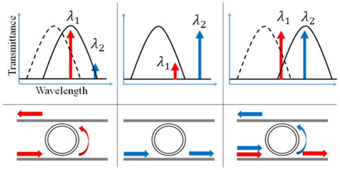
Figure 6. Schematic illustration of an all-optical switch made of an add-drop microring resonator. The dotted line represents the transmittance spectrum of a cold cavity. The solid line is the transmittance when inputs are applied. A resonant shift occurs due to the optical Kerr effect. Two different wavelengths λ1, and λ2 are used for the operation. (a) λ1 will drop (high) when only λ1 is inputted (high). (b) λ2 will not drop (low) when only λ2 is inputted (high). (c) λ2 will drop (high) when both λ1 and λ2 are inputted (high). As a result, λ2 can be switched off and on by turning λ1 signal on and off. Reprinted with permission from [71] © The Optical Society.
The basic building block of an optical flip-flop device is the optical bistable switch. In this device, the output of the system takes on one of two possible states, depending on the states of the inputs. Optical bistable operation permits optical read–write memory operation, opening the possibility of an integrated optical logic circuit on a single chip. A typical way of forming a bistable optical device is to place a saturable absorber inside a resonator. As the input intensity is increased, the field inside the cavity also increases, lowering the absorption of material and thus increasing the field intensity further. If the intensity of the incident field is subsequently lowered, the field inside the cavity tends to remain large because the absorption of the material system has again been reduced. However, even if single bistable switches have already been demonstrated on different platforms, it is worth noting that the next big challenge is the realization of a complex system, where a number of bistable switches are connected in tandem and in parallel [73][74][75][76][77][78][79][80][73-80].
Electronic transistors, as the basic unit of logic circuits, have succeeded in supporting large-scale integrated circuits for computers. Any complex logic circuit can express a combination of three basic logic gates, AND, OR, and NOT, and these basic gates can be constructed with a universal transistor. Although electronic logic gates have enabled creation of integrated circuits with high density and functionality, optical logic gates cannot reach the far requirements of large-scale optical computing circuits even today [81]. On the other hand, optical transistors, as the core hardware of optical gates, so far have not been effectively exploited. Moreover, the universal optical transistor does not seem to exist or be practical for optical gates. Many different approaches to optical transistors have been proposed. Much early work was based on optical bistability [82] using nonlinear optical phenomena, mostly in resonators, whereas others worked on the optically controlled switching of light-exploiting single molecules [83] or quantum dots [84].
Today, in optical networks, data are encoded on photons for transmission, while information processing is often carried out through optical–electrical–optical (OEO) conversions. In the last 20 years, with the aim to assist/replace some of the electronic modules used in network routers, optical signal processing systems (OSPs) have been investigated. OSP refers to a broad range of techniques with the aim to process and manipulate the signal, i.e., amplitude, phase, wavelength, and polarization of optical waves, directly in the optical domain. Optical signal processing techniques employ a wide range of devices and various nonlinearities to achieve multiple network functionalities. Widely used functionalities demonstrated in nonlinear PICs include wavelength [85][86][87][88][85-88] and format conversions [89], routing [90], phase-sensitive amplification [91], optical multiplexing and demultiplexing [92][93][94][95][96][92-96], optical memory[97] [97], all-optical tunable delay [98], and signal regeneration [99]. Thus far, most of the existing OSP research has relied on third-order nonlinearities, such as four-wave mixing (FWM), self-phase modulation (SPM), and cross-phase modulation (XPM) [100][101][102][103][104][105][100-105].
As an example, C-band wavelength conversion in Si photonic wire waveguides with submicron cross-section was demonstrated by means of nondegenerate FWM (see fig. 7) [105]). The nonresonant character of the FWM allowed to demonstrate frequency tuning of the idler from ∼ 20 GHz to > 100 GHz, thus covering several C-band DWDM channels.
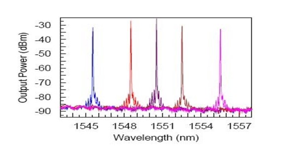
Figure 7 Output spectra from a single-mode silicon photonic-wire waveguide with a cross- section of 220 nm × 445 nm and length of L = 4.2 mm fabricated on a SOI. Pump (λp ~1435 nm) and signal laser sources were multiplexed and launched into the waveguide using a tapered fiber in copropagating configuration; several signal wavelengths (λs =1545.5, 1548.5, 1550.5, 1552.5, and 1555.5 nm) were used. On each side of the signal wavelength employed, newly-generated satellite peaks are clearly seen. Reprinted with permission from [105] © The Optical Society
Current optical networks are mostly based on time-division-multiplexing (TDM) and wavelength-division-multiplexing (WDM). In the former, multiple relatively low-bit-rate streams of data with the same carrier frequency are interleaved to create a single high-bit-rate stream, while the latter involves simultaneous propagation of multiple data signals, each at a different wavelength in a single optical line. Wavelength-division-multiplexing (WDM) techniques offer very effective utilization of the fiber bandwidth directly in the wavelength domain. A first issue of current optical networks concerns wavelength-blocking. In order to overcome it, a fundamental piece is represented by wavelength conversion devices. They can be obtained using different nonlinear effects, such as FWM or XPM [100-105]. Another issue is to increase transmission bandwidth, and an option is to combine TDM and WDM. In this process, demultiplexing an ultra-high-data-rate time-multiplexed signal to speeds receivable through electronics is achieved by wavelength conversion. Specifically, information multiplexed in the time domain through optical time demultiplexing (OTDM) can be converted into parallel lower-data-rate wavelength or spatial channels. This process has been achieved utilizing FWM, whereby a relatively low repetition rate pump switches out temporally multiplexed channels by converting them to new wavelengths (the idler in the FWM process) [92][93][94][95][96][92-96]. There are, of course, other routes that can be followed to increase transmission bandwidth and/or to develop advanced processing chips. The goal of increasing bandwidth density of on-chip interconnects without increasing the number of waveguides, waveguide crossings, and chip footprint, for instance, may be reached by exploiting mode-division-multiplexing (MDM) in conjunction with WDM. Polarization-division-multiplexing (PDM) and orthogonal frequency-division-multiplexing (OFDM) are two other effective methods to increase the spectral efficiency of a communication system [96].
When signal modulation rate increases, signal degradation in the optical channel caused by dispersion, nonlinearity, and noise becomes a critical issue. Conventionally, signal regeneration in an optical system is performed through optical–electrical–optical (OEO) conversion, in which a weak and distorted signal is detected, restored in electronics, and retransmitted onto an optical fiber. Regenerators are designed to increase system performance, reduce data degradation, and enhance signal-to-noise ratio (SNR) for higher link capacity. In general, regenerators perform three signal processing functions: (1) reamplifying, (2) reshaping, and (3) retiming the signal. When the data rate is becoming higher and higher (towards 100 Gb/s), optoelectronic regeneration schemes will be very hard to implement or even impossible. Thus, all-optical regeneration, either 2R (re-amplification, re-shaping) or 3R (re-amplification, re-shaping, re-timing), has become a key technology to improve signal quality [99].
Finally, nonlinear optical sources provide an outstanding example of new possibilities offered by integrated nonlinear photonic chips, such as generation of new classes, named supercontinuum generation [106], and microcombs [107], which are capable of generating coherent, ultra-broadband light sources that cannot be produced in linear photonic systems.
Supercontinuum generation is a device functionality that has important applications in many areas of photonic integrated circuits, particularly in WDM applications. As an example, it could be beneficial to use a single broadband laser source, select by filtering specific wavelength channels, and then modulate these channels instead of using a separate laser for each wavelength. An experimental demonstration of a tunable continuum source in silicon photonic wires (SPWs) with a power-dependent broad spectrum was reported in [108]. As can be seen in Figure 14, a spectral broadening of more than 350 nm was observed upon propagation of ultrashort 1.3 μm wavelength optical pulses in a 4.7 mm long single-mode waveguide.
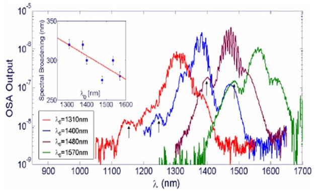
Figure 8. Supercontinuum generation in a 4.7-mm-long silicon-photonic-wire waveguide for several input central wavelengths at P 0 ≈ 1W. The inset shows that the spectral broadening increases as λ0 approaches the ZGVD wavelength of 1290 nm. Reprinted with permission from [108] © The Optical Society
Optical frequency combs (OFCs) are often referred to as optical rulers: their spectra consist of a precise sequence of discrete and equally spaced spectral lines that represent precise marks in frequency. This discrete ensemble of equally spaced laser frequencies that distinguish OFCs from other light sources is the spectral counterpart of the regular train of short pulses emitted by mode-locked lasers. The OFCs solve the challenge of directly measuring optical frequencies and are now exploited as the most accurate time references available, ready to replace the current standard for time. Laser frequency combs can provide integrated sources of mutually coherent laser lines for terabit-per-second transceivers, parallel coherent light detection, or photonics-assisted signal processing. Mode-locked lasers were initially used for comb generation. Thereafter, comb emission was demonstrated in continuous-wave (cw) laser-pumped resonators through cascaded third-order parametric processes [109]. Because of the relatively low strength of third-order nonlinearity, generation of Kerr combs requires small interaction volumes and high-Q resonators. For these reasons, small resonators are particularly suited to reach broadband comb generation with quite moderate pump power. Advancements in the fabrication technology of optical micro-cavities may enable realizing ultra-fast and stable optical clocks and pulsed sources with extremely high repetition-rates in the form of compact and integrated devices. In this framework, demonstration of planar high-Q resonators, compatible with silicon technology [110][111][110, 111], has revealed a unique opportunity for these devices to provide entirely new capabilities for photonic-integrated technologies. It can also be recalled that electro-optic (EO) modulation, in materials with second-order nonlinearity, provides an interesting alternative to Kerr (third-order nonlinearity) resonators for the generation of OFCs; the electrical controllability of EO combs guarantees a greater versatility and also an excellent comb stability and phase coherence [112].
References
- Miller, S. E. Integrated Optics: An Introduction. Bell Syst. Tech. J., 1969, 48, 2059-2069.
- Koch, T.L.; Koren, U. Semiconductor photonic integrated circuits. IEEE J. Quant. Electron., 1991, 27, 641-653
- Nagarajan, R.; Joyner, C.H.; Schneider, R.P.; Bostak, J.S.; Butrie, T.; Dentai, A.G.; Dominic V. Large-scale photonic integrated circuits. IEEE J. Sel. Topics Quant. Electron., 2005, 11, 50-65.
- Righini, G.C.; Ferrari, M., Eds. Integrated Optics. Volume 1: Modeling, material platforms and fabrication techniques, The IET, London, UK, 2020.
- Righini, G.C.; Ferrari, M., Eds. Integrated Optics. Volume 2: Characterization, devices and applications, The IET, London, UK, 2020.
- Anderson, D. B.; Boyd, J. T. Wideband CO2 Laser Second Harmonic Generation Phase Matched in GaAs Thin‐Film Waveguides. Phys. Lett., 1971, 19, 266.
- Chen, Z.; Morandotti, R. Nonlinear Photonics and Novel Optical Phenomena, Springer, New York, USA, 2012.
- Hendrickson, S.M.; Foster, A.C.; Camacho, R.M.; Clader, B.D. Integrated nonlinear photonics: emerging applications and ongoing challenges. Optical Soc. Am. B, 2014, 31, 3193–3203.
- Ji, X.; Liu, J.; He, J.; Wang, R.N.; Qiu, Z.; Riemensberger, J.; Kippenberget, T.J. Compact, spatial-mode-interaction-free, ultralow-loss, nonlinear photonic integrated circuits. Commun Phys, 2022, 5, 84.
- Koshelev, K.; Kruk, S.; Melik-Gaykazyan E.; Jae-Hyuck Choi, J.H.; Andrey Bogdanov, A.; Hong-Gyu Park, H.-G.; Kivshar, Y. Subwavelength dielectric resonators for nonlinear nanophotonics. Science, 2020, 367, 288-92
- Caspani, L.; Duchesne, D.; Dolgaleva, K.; Wagner, S.J.; Ferrera, M.; Razzari, L.; Pasquazi, A.; Peccianti, M.; Moss, D.J.; Aitchison, J.S.; Morandotti, R. Optical frequency conversion in integrated devices. Opt. Soc. Am. B, 2011, 28, A67-A82.
- Giancarlo Righini, Luigi Sirleto. Advances in Nonlinear Photonics. Woodhead Publishing May 2023.
- Selvaraja, K.; Sethi, P. Review on Optical Waveguides. In Emerging Waveguide Technology; You, K.Y., Ed.; IntechOpen: Rijeka, Croatia, 2018.
- Tsuchizawa, T.; Yamada, K.; Fukuda, H.; Watanabe, T.; Takahashi, J.; Takahashi, M.; Shoji, T.; Tamechika, E.; Itabashi, S.; Morita, H. Microphotonics devices based on silicon microfabrication technology. IEEE J. Selected Topics Quant. Electr., 2005, 11, 232-240.
- Gerard, J.-M.; Sermage, B.; Gayral, B.; Legrand, B.; Costard, E.; Thierry-Mieg, V. Enhanced Spontaneous Emission by Quantum Boxes in a Monolithic Optical Microcavity. Rev. Lett., 1998, 81, 1110–1113.
- Butt, M.A.; Khonina, S.N.; Kazanskiy, N.L. Recent advances in photonic crystal optical devices: A review. Optics & Laser Technology, 2021, 142, 107265.
- Righini, G.C.; Dumeige, Y.; Féron, P.; Ferrari, M.; Nunzi Conti, G.; Ristic, D.; Soria, S. Whispering gallery mode microresonators: Fundamentals and applications. Nuovo Cim., 2011, 34, 435–488.
- Frigenti, G; Farnesi, D.; Nunzi Conti, G.; Soria S. Nonlinear Optics in Microspherical Resonators. Micromachines, 2020, 11, 303.
- Lin, G.; Coillet, A.; Chembo, Y. K. Nonlinear photonics with high-Q whispering-gallery-mode resonators. Opt. Photon., 2017, 9, 828-890.
- Strekalov1, D.V.; Marquardt, C.; Matsko, A.B.; Harald G L Schwefel, H.G.L.; Leuchs, G. Nonlinear and quantum optics with whispering gallery resonators. Opt., 2016, 18, 123002
- Kuo, P.; Bravo-Abad, J.; Solomon, G. Second-harmonic generation using quasi-phasematching in a GaAs whispering-gallery-mode microcavity. Com., 2014, 5, 3109.
- Rostami, A.; Ahmadi, H.; Heidarzadeh, H.; Taghipour, A. Microsphere and Fiber Optics based Optical Sensors. In Optical Sensors – New Developments and Practical Applications, Editors Yasin, M.; Harun, S. W.; Arof, H. IntechOpen, Croatia, 2014.
- Slusher, R. E.; Eggleton, B.J. Nonlinear Photonic Crystals, Springer Berlin, Heidelberg, 2003.
- Soljačić, M.; Joannopoulous, J. D. Enhancement of nonlinear effect using photonic crystals. Mater., 2004, 3, 212–9
- Zhang, Y.; Sheng, Y.; Zhu, S.; Xiao, M.; Krolikowski, W. Nonlinear photonic crystals: from 2D to 3D. Optica, 2021, 8, 372-381.
- Pan, J.; Fu, M.; Yi, W.; Wang, X.; Liu, J.; Zhu, M.; Qi, J.; Yin, S.; Huang, G.; Zhu, S.; Chen, X.; Tang, W.; Liao, J.; Yang, H.; Li, X. Improving Low-Dispersion Bandwidth of the Silicon Photonic Crystal Waveguides for Ultrafast Integrated Photonics. Photonics, 2021, 8, 105.
- Bozhevolnyi, S. I.; Volkov, V. S.; Devaux, E.; Laluet, J.-Y.; Ebbesen, T. W. Channel plasmon subwavelength waveguide components including interferometers and ring resonators. Nature, 2006, 440, 508–511.
- Holmström, P.; Thylén, L.; Bratkovsky, A. Composite metal/ quantum-dot nanoparticle-array waveguides with compensated loss. Phys. Lett., 2010, 97, 073110.
- Panoiu, N. C.; Sha, W.E.I.; Lei, D.Y.; Li, G.-C. Nonlinear optics in plasmonic nanostructures. Opt., 2018, 20, 083001.
- Kuznetsov, A.I.; Miroshnichenko, A.E. Brongersma, M.L.; Kivshar, Y. S.; Luk’yanchuk, B. Optically resonant dielectric nanostructures. Science, 2016, 354, aag2472.
- Staude, I.; Schilling, J. Metamaterial-inspired silicon nanophotonics. Nature Photon., 2017, 11, 274–284.
- Yang, Z.J.; Jiang, R.; Zhuo. X.; Xie, Y.-M.; Wang, J.; Lin, H.-Q. Dielectric nanoresonators for light manipulation. Rep., 2017, 701, 1–50.
- Kruk, S; Kivshar, Y.S. Functional meta-optics and nanophotonics governed by Mie resonances. ACS Photonics, 2017, 4, 2638-2649.
- Wang, J., Du, J. Metasurfaces for Spatial Light Manipulation. In Metamaterials-Devices and Applications, Intech Open, Borja, A.L., Ed., Croatia, 2017.
- Quaranta, G.; Basset, G.; Martin, O.J.; Gallinet, B. Recent advances in resonant waveguide grating. Laser Photonics Rev., 2018, 2, 1800017.
- Yu, Z.; Xi, X.; Ma, J.; Tsang, H. K.; Zou, C.L.; Sun, X. Photonic integrated circuits with bound states in the continuum. Optica, 2019, 6, 1342-1348.
- Kivshar, Y. All-dielectric meta-optics and non-linear nanophotonics, National Science Review, 2018, 5, 144–158.
- Bonacina, L.; Brevet, P.F.; Finazzi, M.; Celebrano, M. Harmonic generation at the nanoscale. Appl. Phys., 2020, 127, 230901.
- Sain, B.; Meier, C.; Zentgraf, T. Nonlinear optics in all-dielectric nanoantennas and metasurfaces: A review. Photonics, 2019, 1, 024002.
- Koshelev, K.; Kruk, S.; Melik-Gaykazyan, E.; Choi, J.H.; Bogdanov, A.; Park, H.G.; Kivshar, Y. Subwavelength dielectric resonators for nonlinear nanophotonics. Science, 2020, 367, 288–292.
- Raghunathan, V.; Deka, J.; Menon, S.; Biswas, R.; A.S, L.K. Nonlinear Optics in Dielectric Guided-Mode Resonant Structures and Resonant Metasurfaces. Micromachines, 2020, 11, 449.
- Han, Z.; Ding, F.; Cai, Y.; Levy, U. Significantly enhanced second-harmonic generations with all-dielectric antenna array working in the quasi-bound states in the continuum and excited by linearly polarized plane waves. Nanophotonics, 2021, 10, 1189–1196.
- Zhang, X.; He, L.; Gan, X.; Huang, X.; Du, Y.; Zhai, Z.; Li, Z.; Zheng, Y.; Chen, X; Cai, Y.; Ao, X. Quasi-Bound States in the Continuum Enhanced Second-Harmonic Generation in Thin-Film Lithium Niobate. Laser & Photonics Reviews, 2022, 16, 2200031.
- Sirleto, L.; Righini, G.C. An Introduction to Nonlinear Integrated Photonics Devices: Nonlinear Effects and Materials. Micromachines 2023, 14, 604.
- He, ; Zhang, F.; Zhang, H.; Kong, L.-J.; Zhang, W.; Xu, X.; Zhang, X. Topology-Optimized Ultracompact All-Optical Logic Devices on Silicon Photonic Platforms. ACS Photonics 2022, 9, 597–604.
- Margalit, ; Xiang, C.; Bowers, S.M.; Bjorlin, A.; Blum, R.; Bowers, J.E. Perspective on the future of silicon photonics and electronics. Appl. Phys. Lett. 2021, 118, 220501.
- Osgood, M.; Panoiu, N.C.; Dadap, J.I.; Liu, X.; Chen, X.; Hsieh, I.-W.; Dulkeith, E.; Green, W.M.J.; Vlasov, Y.A. Engineering nonlinearities in nanoscale optical systems: Physics and applications in dispersion-engineered silicon nanophotonic wires. Adv. Opt. Photon. 2009, 1, 162–235.
- Leuthold, ; Koos, C.; Freude, W. Nonlinear silicon photonics. Nat. Photonics 2010, 4, 535–544.
- Nikdast, ; Pasricha, S.; Nicolescu, G.; Seyedi, A.; Liang, D. Silicon Photonics for High-Performance Computing and Beyond; CRC Press: Boca Raton, FL, USA, 2021.
- Saeidi, ; Awan, K.M.; Sirbu, L.; Dolgaleva, K. Nonlinear photonics on-a-chip in III-V semiconductors: Quest for promising material candidates. Appl. Opt. 2017, 56, 5532–5541.
- Vyas, ; Espinosa, D.H.G.; Hutama, D.; Jain, S.K.; Mahjoub, R.; Mobini, E.; Awan, K.M.; Lundeen, J.; Dolgaleva, K. Group III-V semiconductors as promising nonlinear integrated photonic platforms. Adv. Phys. X 2022, 7, 2097020.
- Mobini, ; Espinosa, D.H.G.; Vyas, K.; Dolgaleva, K. AlGaAs Nonlinear Integrated Photonics. Micromachines 2022, 13, 991.
- Liu, ; Sun, C.; Xiong, B.; Wang, L.; Wang, J.; Wang, Y.; Hao, Z.; Li, H.; Luo, Y.; Yan, J.; et al. Aluminum nitride-on-sapphire platform for integrated high-Q microresonators. Opt. Express 2017, 25, 587.
- Xiong, ; Pernice, W.; Ryu, K.; Schuck, C.; Fong, K.Y.; Palacios, T.; Tang, H.X. Integrated GaN photonic circuits on silicon (100) for second harmonic generation. Opt. Express 2011, 19, 10462–10470.
- Lake, P.; Mitchell, M.; Jayakumar, H.; dos Santos, L.F.; Curic, D.; Barclay, P.E. Efficient telecom to visible wavelength conversion in doubly resonant gallium phosphide microdisks. Appl. Phys. Lett. 2016, 108, 031109.
- Luo, ; Jiang, H.; Rogers, S.; Liang, H.; He, Y.; Lin, Q. On-chip second-harmonic generation and broadband parametric down-conversion in a lithium niobate microresonator. Opt. Express 2017, 25, 24531–24539.
- Boes, ; Corcoran, B.; Chang, L.; Bowers, J.; Mitchell, A. Status and potential of lithium niobate on insulator (LNOI) for photonic integrated circuits. Laser Photon. Rev. 2018, 12, 1700256.
- Vazimali, G.; Fathpour, S. Applications of thin-film lithium niobate in nonlinear integrated photonics. Adv. Photonics 2022, 4, 034001.
- Kaur, ; Boes, A.; Ren, G.; Nguyen, T.G.; Roelkens, G.; Mitchell, A. Hybrid and heterogeneous photonic integration. APL Photonics 2021, 6, 061102.
- Fathpour, Heterogeneous Nonlinear Integrated Photonics. IEEE J. Quantum Electron. 2018, 54, 6300716.
- Fathpour, Emerging heterogeneous integrated photonic platforms on silicon. Nanophotonics 2015, 4, 143–164.
- Xing, ; Ma, D.; Ooi, K.J.; Choi, J.W.; Agarwal, A.M.; Tan, D. CMOS-compatible PECVD silicon carbide platform for linear and nonlinear optics. ACS Photonics 2019, 6, 1162−1167.
- Castelletto, ; Rosa, L.; Johnson, B.C. Silicon carbide for novel quantum technologies devices. In Advanced silicon carbide devices and processing; Chapter 9; Saddow, S., La Via, F., Eds.; Intech Open: London, UK, 2015.
- Guidry, A.; Yang, K.Y.; Lukin, D.M.; Markosyan, A.; Yang, J.; Fejer, M.M.; Vučković, J. Optical parametric oscillation in silicon carbide nanophotonics. Optica 2020, 7, 1139–1142.
- Sirleto, L.; Righini, G.C. An Introduction to Nonlinear Integrated Photonics: Structures and Devices. Micromachines 2023, 14, 614.
- Grinblat, ; Zhang, H.; Nielsen, M.P.; Krivitsky, L.; Berté, R.; Li, Y.; Tilmann, B.; Cortés, E.; Oulton, R.F.; Kuznetsov, A.I.; et al. Efficient Ultrafast All-Optical Modulation in a Nonlinear Crystalline Gallium Phosphide Nanodisk at the Anapole Excitation. Sci. Adv. 2020, 6, eabb3123.
- Vlachos, ; Raffaelli, C.; Aleksic, S.; Andriolli, N.; Apostolopoulos, D.; Avramopoulos, H.; Erasme, D.; Klonidis, D.; Petersen, M.N.; Scaffardi, M.; et al. Photonics in switching: Enabling technologies and subsystem design. J. Opt. Netw. 2009, 8, 404–428.
- Sasikala, ; Chitra, K. All optical switching and associated technologies: A review. J. Opt. 2018, 47, 307–317.
- Lu, ; Liu, X.; Wang, L.; Gong, Y.; Mao, D. Ultrafast all-optical switching in nanoplasmonic waveguide with Kerr nonlinear resonator. Opt. Express 2011, 19, 2910–2915.
- Pelc, S.; Rivoire, K.; Vo, S.; Santori, C.; Fattal, D.A.; Beausoleil, R.G. Picosecond all-optical switching in hydrogenated amorphous silicon microring resonators. Opt. Express 2014, 22, 3797–3810.
- Fushimi, ; Tanabe, T. All-optical logic gate operating with single wavelength. Opt. Express 2014, 22, 4466–4479.
- Chhipa, K.; Madhav, B.T.P.; Suthar, B. An all-optical ultracompact microring-resonator-based optical switch. J. Comput. Electron. 2021, 20, 419–425.
- Notomi, ; Shinya, A.; Mitsugi, S.; Kira, G.; Kuramochi, E.; Tanabe. T. Optical bistable switching action of Si high-Q photonic-crystal nanocavities. Opt. Express 2005, 13, 2678–2687.
- Wu, -D.; Shih, T.T.; Chen, M.-H. New all-optical logic gates based on the local nonlinear Mach-Zehnder interferometer. Opt. Express 2008, 16, 248–257.
- Fushimi, ; Tanabe, T. All-optical logic gate operating with single wavelength. Opt. Express 2014, 22, 4466–4479.
- Xiaoyu, ; Xiaoyong, H.; Hong, Y.; Qihuang, G. Ultracompact all-optical logic gates based on nonlinear plasmonic nanocavities. Nanophotonics 2017, 6, 365–376.
- Jandieri, ; Khomeriki, R.; Onoprishvili, T.; Werner, D.H.; Berakdar, J.; Erni, D. Functional all-optical logic gates for true time-domain signal processing in nonlinear photonic crystal waveguides. Opt. Express 2020, 28, 18317–18331.
- Anagha, G.; Jeyachitra, R.K. Review on all-optical logic gates: Design techniques and classifications—Heading toward high-speed optical integrated circuits. Opt. Eng. 2022, 61, 060902.
- Thankaraj, S.; Ramasamy, A. Revolution of optical computing logic gates based on its applications: An extensive survey. Opt. Eng. 2022, 61, 110901.
- Jiao, M.; Liu, J.W.; Zhang, L.W.; Yu, F.H.; Zuo, G.M.; Zhang, J.; Zhao, F.; Lin, W.; Shao, L. All-optical logic gate computing for high-speed parallel information processing. Opto-Electron. Sci. 2022, 1, 220010.
- Miller, A. Are optical transistors the logical next step? Nat. Photon. 2010, 4, 3–5.
- Gibbs, M. Optical Bistability: Controlling Light with Light; Academic Press: Cambridge, MA, USA, 1985.
- Hwang, ; Pototschnig, M.; Lettow, R.; Zumofen, G.; Renn, A.; Götzinger, S.; Sandoghdar, V. A single-molecule optical transistor. Nature 2009, 460, 76–80.
- Fushman, ; Englund, D.; Faraon, A.; Stoltz, N.; Petroff, P.; Vuckovic, J. Controlled Phase Shifts with a Single Quantum Dot. Science 2008, 320, 769–772.
- Yoo, J.B. Wavelength conversion technologies for WDM network applications. J. Light. Technol. 1996, 14, 955–966.
- Petrillo, G.; Foster, M.A. Full 160-Gb/s OTDM to 16x10-Gb/s WDM conversion with a single nonlinear interaction. Opt. Express 2013, 21, 508–518.
- Lacava, ; Ettabib, M.; Cristiani, I.; Fedeli, J.; Richardson, D.; Petropoulos, P. Ultra-Compact Amorphous Silicon Waveguide for Wavelength Conversion. IEEE Photonics Technol. Lett. 2016, 28, 410–414.
- Zheng, ; Chen, X. Nonlinear wave mixing in lithium niobate thin film. Adv. Phys. X 2021, 6, 1889402.
- Guo, ; Wu, B.; Wang, Y.; Wen, F.; Geng, Y.; Zhou, H.; Qiu, K. On-chip Mach Zehnder interferometer-based all-optical amplitude regenerator for optical 16-QAM signals. Opt. Express 2021, 29, 27683–27695.
- Singh, ; Iadicicco, A.; Agrawal, N.; Saha, C.; Chauhan, R. A compact formulation of all optical signal router by using plasmonic waveguides. Opt. Quant. Electron. 2022, 54, 478.
- Yan, ; He, H.; Liu, H.; Iu, M.; Ahmed, O.; Chen, E.; Blakey, P.; Akasaka, Y.; Ikeuchi, T.; Helmy, A.S. χ(2)-based AlGaAs phase sensitive amplifier with record gain, noise, and sensitivity. Optica 2022, 9, 56–60.
- Pelusi, ; Ta’Eed, V.; Lamont, M.; Madden, S.; Choi, D.-Y.; Luther-Davies, B.; Eggleton, B. Ultra-High Nonlinear As2S3 Planar Waveguide for 160-Gb/s Optical Time-Division Demultiplexing by Four-Wave Mixing. IEEE Photonics Technol. Lett. 2007, 19, 1496–1498.
- Palushani, ; Hansen Mulvad, H.; Galili, M.; Hu, H.; Oxenlowe, L.K.; Clausen, A.T.; Jeppesen, P. OTDM-to-WDM conversion based on time-to frequency mapping by time-domain optical Fourier transformation. IEEE J. Sel. Top. Quant. Electron. 2012, 18, 681–688.
- Hansen Mulvad, C.; Palushani, E.; Hu, H.; Ji, H.; Lillieholm, M.; Galili, M.; Clausen, A.T.; Pu, M.; Yvind, K.; Hvam, J.M.; et al. Ultra-high-speed optical serial-to-parallel data conversion by time domain optical Fourier transformation in a silicon nanowire. Opt. Express 2011, 19, B825–B835.
- Luo, W.; Ophir, N.; Chen, C.P.; Gabrielli, L.H.; Poitras, C.B.; Bergmen, K.; Lipson, M. WDM-compatible mode-division multiplexing on a silicon chip. Nat. Commun. 2014, 5, 3069.
- Jansen, L.; Morita, I.; Schenk, T.C.; Tanaka, H. Long-haul transmission of16×52.5 Gbits/s polarization-division- multiplexed OFDM enabled by MIMO processing (Invited). J. Opt. Netw. 2008, 7, 173–182.
- Hill, T.; Dorren, H.J.S.; Vries, T.; Leijtens, X.J.M.; Besten, J.H.; Smalbrugge, B.; Oei, Y.-S.; Binsma, H.; Khoe, G.-D.; Smit, M.K. A fast low-power optical memory based on coupled micro-ring lasers. Nature 2004, 432, 206–209.
- Kowsari, ; Ahmadi, V.; Darvish, G.; Moravvej-Farshi, M.K. All-optical tunable delay line based on nonlinearities in a chalcogenide microfiber coil resonator. J. Opt. Soc. Am. B 2017, 34, 1199–1205.
- Ciaramella, Wavelength Conversion and All-Optical Regeneration: Achievements and Open Issues. J. Light. Technol. 2012, 30, 572–582.
- Willner, E.; Yilmaz, O.F.; Wang, J.; Wu, X.; Bogoni, A.; Zhang, L.; Nuccio, S.R. Optically Efficient Nonlinear Signal Processing. IEEE J. Sel. Top. Quant. Electron. 2011, 17, 320–332.
- Lacava, ; Ettabib, M.A.; Petropoulos, P. Nonlinear Silicon Photonic Signal Processing Devices for Future Optical Networks. Appl. Sci. 2017, 7, 103.
- Wang, ; Long, Y. On-chip silicon photonic signaling and processing: A review. Sci. Bull. 2018, 63, 1267–1310.
- Minzioni, ; Lacava, C.; Tanabe, T.; Dong, J.; Hu, X.; Csaba, G.; Porod, W.; Singh, G.; Willner, A.E.; Almaiman, A.; et al. Roadmap on all-optical processing. J. Opt. 2019, 21, 063001.
- Chang, ; Boes, A.; Shu, H.; Xie, W.; Huang, H.; Qin, J.; Shen, B.; Wang, X.; Mitchell, A.; Bowers, J. EL. Second Order Nonlinear Photonic Integrated Platforms for Optical Signal Processing. IEEE J. Sel. Top. Quant. Electron. 2021, 27, 1–11.
- Espinola, L.; Dadap, J.I.; Osgood, R.M.; McNab, S.J.; Vlasov, Y. C-band wavelength conversion in silicon photonic wire waveguides. Opt. Express 2005, 13, 4341–4349.
- Dudley, M.; Genty, G.; Coen, S. Supercontinuum generation in photonic crystal fiber. Rev. Mod. Phys. 2006, 78, 1135–1184.
- Gaeta, L.; Lipson, M.; Kippenberg, T.J. Photonic-chip-based frequency combs. Nat. Photonics 2019, 13, 158–169.
- Hsieh, -W.; Chen, X.; Liu, X.; Dadap, J.I.; Panoiu, N.C.; Chou, C.-Y.; Xia, F.; Green, W.M.; Vlasov, Y.A.; Osgood, R.M. Supercontinuum generation in silicon photonic wires. Opt. Express 2007, 15, 15242–15249.
- Del’Haye, ; Schliesser, A.; Arcizet, O.; Wilken, T.; Holzwarth, R.; Kippenberg, T.J. Optical frequency comb generation from a monolithic microresonator. Nature 2007, 450, 1214–1217.
- Ferdous, ; Miao, H.; Leaird, D.E.; Srinivasan, K.; Wang, J.; Chen, L.; Varghese, L.T.; Weiner. Spectral line-by-line pulse shaping of on-chip microresonator frequency combs. Nat. Photon. 2011, 5, 770–776.
- Razzari, ; Duchesne, D.; Ferrera, M.; Morandotti, R.; Chu, S.; Little, B.; Moss, D. CMOS-compatible integrated optical hyper-parametric oscillator. Nat. Photon. 2010, 4, 41–45.
- Hu, Y.; Yu, M.; Buscaino, B.; Sinclair, N.; Zhu, D.; Cheng, R.; Shams-Ansari, A.; Shao, L.; Zhang, M.; Kahn, J.M.; et al. High-efficiency and broadband on-chip electro-optic frequency comb generators. Nat. Photon. 2022, 16, 679–685.
[1][2][3][4][5][6][7][8][9][10][11][12][13][14][15][16][17][18][19][20][21][22][23][24][25][26][27][28][29][30][31][32][33][34][35][36][11237][38][39][40][41][42][43][44][45][46][47][48][49][50][51][52][53][54][55][56][57][58][59][60][61][62][63][64][65][66][67][68][69][70][71][72][73][74][71][75][76][77][78][79][80][81][82][83][84][85][86][87][88][89][90][91][92][93][94][95][96][97][98][99][100][101][102][103][104][105][106][107][108][109][110][111].
References
- Miller, S. E. Integrated Optics: An Introduction. Bell Syst. Tech. J., 1969, 48, 2059-2069.
- Koch, T.L.; Koren, U. Semiconductor photonic integrated circuits. IEEE J. Quant. Electron., 1991, 27, 641-653
- Nagarajan, R.; Joyner, C.H.; Schneider, R.P.; Bostak, J.S.; Butrie, T.; Dentai, A.G.; Dominic V. Large-scale photonic integrated circuits. IEEE J. Sel. Topics Quant. Electron., 2005, 11, 50-65.
- Righini, G.C.; Ferrari, M., Eds. Integrated Optics. Volume 1: Modeling, material platforms and fabrication techniques, The IET, London, UK, 2020.
- Righini, G.C.; Ferrari, M., Eds. Integrated Optics. Volume 2: Characterization, devices and applications, The IET, London, UK, 2020.
- Anderson, D. B.; Boyd, J. T. Wideband CO2 Laser Second Harmonic Generation Phase Matched in GaAs Thin‐Film Waveguides. Appl. Phys. Lett., 1971, 19, 266.
- Chen, Z.; Morandotti, R. Nonlinear Photonics and Novel Optical Phenomena, Springer, New York, USA, 2012.
- Hendrickson, S.M.; Foster, A.C.; Camacho, R.M.; Clader, B.D. Integrated nonlinear photonics: emerging applications and ongoing challenges. J. Optical Soc. Am. B, 2014, 31, 3193–3203.
- Ji, X.; Liu, J.; He, J.; Wang, R.N.; Qiu, Z.; Riemensberger, J.; Kippenberget, T.J. Compact, spatial-mode-interaction-free, ultralow-loss, nonlinear photonic integrated circuits. Commun Phys, 2022, 5, 84.
- Koshelev, K.; Kruk, S.; Melik-Gaykazyan E.; Jae-Hyuck Choi, J.H.; Andrey Bogdanov, A.; Hong-Gyu Park, H.-G.; Kivshar, Y. Subwavelength dielectric resonators for nonlinear nanophotonics. Science, 2020, 367, 288-92
- Caspani, L.; Duchesne, D.; Dolgaleva, K.; Wagner, S.J.; Ferrera, M.; Razzari, L.; Pasquazi, A.; Peccianti, M.; Moss, D.J.; Aitchison, J.S.; Morandotti, R. Optical frequency conversion in integrated devices. J. Opt. Soc. Am. B, 2011, 28, A67-A82.
- Giancarlo Righini, Luigi Sirleto. Advances in Nonlinear Photonics. Elsevier. Woodhead Publishing May 2023.
- Selvaraja, S.K.; Sethi, P. Review on Optical Waveguides. In Emerging Waveguide Technology; You, K.Y., Ed.; IntechOpen: Rijeka, Croatia, 2018.
- Tsuchizawa, T.; Yamada, K.; Fukuda, H.; Watanabe, T.; Takahashi, J.; Takahashi, M.; Shoji, T.; Tamechika, E.; Itabashi, S.; Morita, H. Microphotonics devices based on silicon microfabrication technology. IEEE J. Selected Topics Quant. Electr., 2005, 11, 232-240.
- Gerard, J.-M.; Sermage, B.; Gayral, B.; Legrand, B.; Costard, E.; Thierry-Mieg, V. Enhanced Spontaneous Emission by Quantum Boxes in a Monolithic Optical Microcavity. Phys. Rev. Lett., 1998, 81, 1110–1113.
- Butt, M.A.; Khonina, S.N.; Kazanskiy, N.L. Recent advances in photonic crystal optical devices: A review. Optics & Laser Technology, 2021, 142, 107265.
- Righini, G.C.; Dumeige, Y.; Féron, P.; Ferrari, M.; Nunzi Conti, G.; Ristic, D.; Soria, S. Whispering gallery mode microresonators: Fundamentals and applications. Riv. Nuovo Cim., 2011, 34, 435–488.
- Frigenti, G; Farnesi, D.; Nunzi Conti, G.; Soria S. Nonlinear Optics in Microspherical Resonators. Micromachines, 2020, 11, 303.
- Lin, G.; Coillet, A.; Chembo, Y. K. Nonlinear photonics with high-Q whispering-gallery-mode resonators. Adv. Opt. Photon., 2017, 9, 828-890.
- Strekalov1, D.V.; Marquardt, C.; Matsko, A.B.; Harald G L Schwefel, H.G.L.; Leuchs, G. Nonlinear and quantum optics with whispering gallery resonators. J. Opt., 2016, 18, 123002
- Kuo, P.; Bravo-Abad, J.; Solomon, G. Second-harmonic generation using quasi-phasematching in a GaAs whispering-gallery-mode microcavity. Nat. Com., 2014, 5, 3109.
- Rostami, A.; Ahmadi, H.; Heidarzadeh, H.; Taghipour, A. Microsphere and Fiber Optics based Optical Sensors. In Optical Sensors – New Developments and Practical Applications, Editors Yasin, M.; Harun, S. W.; Arof, H. IntechOpen, Croatia, 2014.
- Slusher, R. E.; Eggleton, B.J. Nonlinear Photonic Crystals, Springer Berlin, Heidelberg, 2003.
- Soljačić, M.; Joannopoulous, J. D. Enhancement of nonlinear effect using photonic crystals. Nat. Mater., 2004, 3, 212–9
- Zhang, Y.; Sheng, Y.; Zhu, S.; Xiao, M.; Krolikowski, W. Nonlinear photonic crystals: from 2D to 3D. Optica, 2021, 8, 372-381.
- Pan, J.; Fu, M.; Yi, W.; Wang, X.; Liu, J.; Zhu, M.; Qi, J.; Yin, S.; Huang, G.; Zhu, S.; Chen, X.; Tang, W.; Liao, J.; Yang, H.; Li, X. Improving Low-Dispersion Bandwidth of the Silicon Photonic Crystal Waveguides for Ultrafast Integrated Photonics. Photonics, 2021, 8, 105.
- Bozhevolnyi, S. I.; Volkov, V. S.; Devaux, E.; Laluet, J.-Y.; Ebbesen, T. W. Channel plasmon subwavelength waveguide components including interferometers and ring resonators. Nature, 2006, 440, 508–511.
- Holmström, P.; Thylén, L.; Bratkovsky, A. Composite metal/ quantum-dot nanoparticle-array waveguides with compensated loss. Appl. Phys. Lett., 2010, 97, 073110.
- Panoiu, N. C.; Sha, W.E.I.; Lei, D.Y.; Li, G.-C. Nonlinear optics in plasmonic nanostructures. J. Opt., 2018, 20, 083001.
- Kuznetsov, A.I.; Miroshnichenko, A.E. Brongersma, M.L.; Kivshar, Y. S.; Luk’yanchuk, B. Optically resonant dielectric nanostructures. Science, 2016, 354, aag2472.
- Staude, I.; Schilling, J. Metamaterial-inspired silicon nanophotonics. Nature Photon., 2017, 11, 274–284.
- Yang, Z.J.; Jiang, R.; Zhuo. X.; Xie, Y.-M.; Wang, J.; Lin, H.-Q. Dielectric nanoresonators for light manipulation. Phys. Rep., 2017, 701, 1–50.
- Kruk, S; Kivshar, Y.S. Functional meta-optics and nanophotonics governed by Mie resonances. ACS Photonics, 2017, 4, 2638-2649.
- Wang, J., Du, J. Metasurfaces for Spatial Light Manipulation. In Metamaterials-Devices and Applications, Intech Open, Borja, A.L., Ed., Croatia, 2017.
- Quaranta, G.; Basset, G.; Martin, O.J.; Gallinet, B. Recent advances in resonant waveguide grating. Laser Photonics Rev., 2018, 2, 1800017.
- Yu, Z.; Xi, X.; Ma, J.; Tsang, H. K.; Zou, C.L.; Sun, X. Photonic integrated circuits with bound states in the continuum. Optica, 2019, 6, 1342-1348.
- Kivshar, Y. All-dielectric meta-optics and non-linear nanophotonics, National Science Review, 2018, 5, 144–158.
- Bonacina, L.; Brevet, P.F.; Finazzi, M.; Celebrano, M. Harmonic generation at the nanoscale. J. Appl. Phys., 2020, 127, 230901.
- Sain, B.; Meier, C.; Zentgraf, T. Nonlinear optics in all-dielectric nanoantennas and metasurfaces: A review. Adv. Photonics, 2019, 1, 024002.
- Koshelev, K.; Kruk, S.; Melik-Gaykazyan, E.; Choi, J.H.; Bogdanov, A.; Park, H.G.; Kivshar, Y. Subwavelength dielectric resonators for nonlinear nanophotonics. Science, 2020, 367, 288–292.
- Raghunathan, V.; Deka, J.; Menon, S.; Biswas, R.; A.S, L.K. Nonlinear Optics in Dielectric Guided-Mode Resonant Structures and Resonant Metasurfaces. Micromachines, 2020, 11, 449.
- Han, Z.; Ding, F.; Cai, Y.; Levy, U. Significantly enhanced second-harmonic generations with all-dielectric antenna array working in the quasi-bound states in the continuum and excited by linearly polarized plane waves. Nanophotonics, 2021, 10, 1189–1196.
- Zhang, X.; He, L.; Gan, X.; Huang, X.; Du, Y.; Zhai, Z.; Li, Z.; Zheng, Y.; Chen, X; Cai, Y.; Ao, X. Quasi-Bound States in the Continuum Enhanced Second-Harmonic Generation in Thin-Film Lithium Niobate. Laser & Photonics Reviews, 2022, 16, 2200031.Zhang, X.; He, L.; Gan, X.; Huang, X.; Du, Y.; Zhai, Z.; Li, Z.; Zheng, Y.; Chen, X; Cai, Y.; Ao, X. Quasi-Bound States in the Continuum Enhanced Second-Harmonic Generation in Thin-Film Lithium Niobate. Laser & Photonics Reviews, 2022, 16, 2200031.
- Sirleto, L.; Righini, G.C. An Introduction to Nonlinear Integrated Photonics Devices: Nonlinear Effects and Materials. Micromachines 2023, 14, 604.
- He, L.; Zhang, F.; Zhang, H.; Kong, L.-J.; Zhang, W.; Xu, X.; Zhang, X. Topology-Optimized Ultracompact All-Optical Logic Devices on Silicon Photonic Platforms. ACS Photonics 2022, 9, 597–604.
- Margalit, N.; Xiang, C.; Bowers, S.M.; Bjorlin, A.; Blum, R.; Bowers, J.E. Perspective on the future of silicon photonics and electronics. Appl. Phys. Lett. 2021, 118, 220501.
- Osgood, R.M.; Panoiu, N.C.; Dadap, J.I.; Liu, X.; Chen, X.; Hsieh, I.-W.; Dulkeith, E.; Green, W.M.J.; Vlasov, Y.A. Engineering nonlinearities in nanoscale optical systems: Physics and applications in dispersion-engineered silicon nanophotonic wires. Adv. Opt. Photon. 2009, 1, 162–235.
- Leuthold, J.; Koos, C.; Freude, W. Nonlinear silicon photonics. Nat. Photonics 2010, 4, 535–544.
- Nikdast, M.; Pasricha, S.; Nicolescu, G.; Seyedi, A.; Liang, D. Silicon Photonics for High-Performance Computing and Beyond; CRC Press: Boca Raton, FL, USA, 2021.
- Saeidi, S.; Awan, K.M.; Sirbu, L.; Dolgaleva, K. Nonlinear photonics on-a-chip in III-V semiconductors: Quest for promising material candidates. Appl. Opt. 2017, 56, 5532–5541.
- Vyas, K.; Espinosa, D.H.G.; Hutama, D.; Jain, S.K.; Mahjoub, R.; Mobini, E.; Awan, K.M.; Lundeen, J.; Dolgaleva, K. Group III-V semiconductors as promising nonlinear integrated photonic platforms. Adv. Phys. X 2022, 7, 2097020.
- Mobini, E.; Espinosa, D.H.G.; Vyas, K.; Dolgaleva, K. AlGaAs Nonlinear Integrated Photonics. Micromachines 2022, 13, 991.
- Liu, X.; Sun, C.; Xiong, B.; Wang, L.; Wang, J.; Wang, Y.; Hao, Z.; Li, H.; Luo, Y.; Yan, J.; et al. Aluminum nitride-on-sapphire platform for integrated high-Q microresonators. Opt. Express 2017, 25, 587.
- Xiong, C.; Pernice, W.; Ryu, K.; Schuck, C.; Fong, K.Y.; Palacios, T.; Tang, H.X. Integrated GaN photonic circuits on silicon (100) for second harmonic generation. Opt. Express 2011, 19, 10462–10470.
- Lake, D.P.; Mitchell, M.; Jayakumar, H.; dos Santos, L.F.; Curic, D.; Barclay, P.E. Efficient telecom to visible wavelength conversion in doubly resonant gallium phosphide microdisks. Appl. Phys. Lett. 2016, 108, 031109.
- Luo, R.; Jiang, H.; Rogers, S.; Liang, H.; He, Y.; Lin, Q. On-chip second-harmonic generation and broadband parametric down-conversion in a lithium niobate microresonator. Opt. Express 2017, 25, 24531–24539.
- Boes, A.; Corcoran, B.; Chang, L.; Bowers, J.; Mitchell, A. Status and potential of lithium niobate on insulator (LNOI) for photonic integrated circuits. Laser Photon. Rev. 2018, 12, 1700256.
- Vazimali, M.G.; Fathpour, S. Applications of thin-film lithium niobate in nonlinear integrated photonics. Adv. Photonics 2022, 4, 034001.
- Kaur, P.; Boes, A.; Ren, G.; Nguyen, T.G.; Roelkens, G.; Mitchell, A. Hybrid and heterogeneous photonic integration. APL Photonics 2021, 6, 061102.
- Fathpour, S. Heterogeneous Nonlinear Integrated Photonics. IEEE J. Quantum Electron. 2018, 54, 6300716.
- Fathpour, S. Emerging heterogeneous integrated photonic platforms on silicon. Nanophotonics 2015, 4, 143–164.
- Xing, P.; Ma, D.; Ooi, K.J.; Choi, J.W.; Agarwal, A.M.; Tan, D. CMOS-compatible PECVD silicon carbide platform for linear and nonlinear optics. ACS Photonics 2019, 6, 1162−1167.
- Castelletto, S.; Rosa, L.; Johnson, B.C. Silicon carbide for novel quantum technologies devices. In Advanced silicon carbide devices and processing; Chapter 9; Saddow, S., La Via, F., Eds.; Intech Open: London, UK, 2015.
- Guidry, M.A.; Yang, K.Y.; Lukin, D.M.; Markosyan, A.; Yang, J.; Fejer, M.M.; Vučković, J. Optical parametric oscillation in silicon carbide nanophotonics. Optica 2020, 7, 1139–1142.
- Sirleto, L.; Righini, G.C. An Introduction to Nonlinear Integrated Photonics: Structures and Devices. Micromachines 2023, 14, 614.
- Grinblat, G.; Zhang, H.; Nielsen, M.P.; Krivitsky, L.; Berté, R.; Li, Y.; Tilmann, B.; Cortés, E.; Oulton, R.F.; Kuznetsov, A.I.; et al. Efficient Ultrafast All-Optical Modulation in a Nonlinear Crystalline Gallium Phosphide Nanodisk at the Anapole Excitation. Sci. Adv. 2020, 6, eabb3123.
- Vlachos, K.; Raffaelli, C.; Aleksic, S.; Andriolli, N.; Apostolopoulos, D.; Avramopoulos, H.; Erasme, D.; Klonidis, D.; Petersen, M.N.; Scaffardi, M.; et al. Photonics in switching: Enabling technologies and subsystem design. J. Opt. Netw. 2009, 8, 404–428.
- Sasikala, V.; Chitra, K. All optical switching and associated technologies: A review. J. Opt. 2018, 47, 307–317.
- Lu, H.; Liu, X.; Wang, L.; Gong, Y.; Mao, D. Ultrafast all-optical switching in nanoplasmonic waveguide with Kerr nonlinear resonator. Opt. Express 2011, 19, 2910–2915.
- Pelc, J.S.; Rivoire, K.; Vo, S.; Santori, C.; Fattal, D.A.; Beausoleil, R.G. Picosecond all-optical switching in hydrogenated amorphous silicon microring resonators. Opt. Express 2014, 22, 3797–3810.
- Fushimi, A.; Tanabe, T. All-optical logic gate operating with single wavelength. Opt. Express 2014, 22, 4466–4479.
- Chhipa, M.K.; Madhav, B.T.P.; Suthar, B. An all-optical ultracompact microring-resonator-based optical switch. J. Comput. Electron. 2021, 20, 419–425.
- Notomi, M.; Shinya, A.; Mitsugi, S.; Kira, G.; Kuramochi, E.; Tanabe. T. Optical bistable switching action of Si high-Q photonic-crystal nanocavities. Opt. Express 2005, 13, 2678–2687.
- Wu, Y.-D.; Shih, T.T.; Chen, M.-H. New all-optical logic gates based on the local nonlinear Mach-Zehnder interferometer. Opt. Express 2008, 16, 248–257.
- Xiaoyu, Y.; Xiaoyong, H.; Hong, Y.; Qihuang, G. Ultracompact all-optical logic gates based on nonlinear plasmonic nanocavities. Nanophotonics 2017, 6, 365–376.
- Jandieri, V.; Khomeriki, R.; Onoprishvili, T.; Werner, D.H.; Berakdar, J.; Erni, D. Functional all-optical logic gates for true time-domain signal processing in nonlinear photonic crystal waveguides. Opt. Express 2020, 28, 18317–18331.
- Anagha, E.G.; Jeyachitra, R.K. Review on all-optical logic gates: Design techniques and classifications—Heading toward high-speed optical integrated circuits. Opt. Eng. 2022, 61, 060902.
- Thankaraj, B.S.; Ramasamy, A. Revolution of optical computing logic gates based on its applications: An extensive survey. Opt. Eng. 2022, 61, 110901.
- Jiao, S.M.; Liu, J.W.; Zhang, L.W.; Yu, F.H.; Zuo, G.M.; Zhang, J.; Zhao, F.; Lin, W.; Shao, L. All-optical logic gate computing for high-speed parallel information processing. Opto-Electron. Sci. 2022, 1, 220010.
- Miller, D.A. Are optical transistors the logical next step? Nat. Photon. 2010, 4, 3–5.
- Gibbs, H.M. Optical Bistability: Controlling Light with Light; Academic Press: Cambridge, MA, USA, 1985.
- Hwang, J.; Pototschnig, M.; Lettow, R.; Zumofen, G.; Renn, A.; Götzinger, S.; Sandoghdar, V. A single-molecule optical transistor. Nature 2009, 460, 76–80.
- Fushman, I.; Englund, D.; Faraon, A.; Stoltz, N.; Petroff, P.; Vuckovic, J. Controlled Phase Shifts with a Single Quantum Dot. Science 2008, 320, 769–772.
- Yoo, S.J.B. Wavelength conversion technologies for WDM network applications. J. Light. Technol. 1996, 14, 955–966.
- Petrillo, K.G.; Foster, M.A. Full 160-Gb/s OTDM to 16x10-Gb/s WDM conversion with a single nonlinear interaction. Opt. Express 2013, 21, 508–518.
- Lacava, C.; Ettabib, M.; Cristiani, I.; Fedeli, J.; Richardson, D.; Petropoulos, P. Ultra-Compact Amorphous Silicon Waveguide for Wavelength Conversion. IEEE Photonics Technol. Lett. 2016, 28, 410–414.
- Zheng, Y.; Chen, X. Nonlinear wave mixing in lithium niobate thin film. Adv. Phys. X 2021, 6, 1889402.
- Guo, B.; Wu, B.; Wang, Y.; Wen, F.; Geng, Y.; Zhou, H.; Qiu, K. On-chip Mach Zehnder interferometer-based all-optical amplitude regenerator for optical 16-QAM signals. Opt. Express 2021, 29, 27683–27695.
- Singh, L.; Iadicicco, A.; Agrawal, N.; Saha, C.; Chauhan, R. A compact formulation of all optical signal router by using plasmonic waveguides. Opt. Quant. Electron. 2022, 54, 478.
- Yan, Z.; He, H.; Liu, H.; Iu, M.; Ahmed, O.; Chen, E.; Blakey, P.; Akasaka, Y.; Ikeuchi, T.; Helmy, A.S. χ(2)-based AlGaAs phase sensitive amplifier with record gain, noise, and sensitivity. Optica 2022, 9, 56–60.
- Pelusi, M.; Ta’Eed, V.; Lamont, M.; Madden, S.; Choi, D.-Y.; Luther-Davies, B.; Eggleton, B. Ultra-High Nonlinear As2S3 Planar Waveguide for 160-Gb/s Optical Time-Division Demultiplexing by Four-Wave Mixing. IEEE Photonics Technol. Lett. 2007, 19, 1496–1498.
- Palushani, E.; Hansen Mulvad, H.; Galili, M.; Hu, H.; Oxenlowe, L.K.; Clausen, A.T.; Jeppesen, P. OTDM-to-WDM conversion based on time-to frequency mapping by time-domain optical Fourier transformation. IEEE J. Sel. Top. Quant. Electron. 2012, 18, 681–688.
- Hansen Mulvad, H.C.; Palushani, E.; Hu, H.; Ji, H.; Lillieholm, M.; Galili, M.; Clausen, A.T.; Pu, M.; Yvind, K.; Hvam, J.M.; et al. Ultra-high-speed optical serial-to-parallel data conversion by time domain optical Fourier transformation in a silicon nanowire. Opt. Express 2011, 19, B825–B835.
- Luo, L.W.; Ophir, N.; Chen, C.P.; Gabrielli, L.H.; Poitras, C.B.; Bergmen, K.; Lipson, M. WDM-compatible mode-division multiplexing on a silicon chip. Nat. Commun. 2014, 5, 3069.
- Jansen, S.L.; Morita, I.; Schenk, T.C.; Tanaka, H. Long-haul transmission of16×52.5 Gbits/s polarization-division- multiplexed OFDM enabled by MIMO processing (Invited). J. Opt. Netw. 2008, 7, 173–182.
- Hill, M.T.; Dorren, H.J.S.; Vries, T.; Leijtens, X.J.M.; Besten, J.H.; Smalbrugge, B.; Oei, Y.-S.; Binsma, H.; Khoe, G.-D.; Smit, M.K. A fast low-power optical memory based on coupled micro-ring lasers. Nature 2004, 432, 206–209.
- Kowsari, A.; Ahmadi, V.; Darvish, G.; Moravvej-Farshi, M.K. All-optical tunable delay line based on nonlinearities in a chalcogenide microfiber coil resonator. J. Opt. Soc. Am. B 2017, 34, 1199–1205.
- Ciaramella, E. Wavelength Conversion and All-Optical Regeneration: Achievements and Open Issues. J. Light. Technol. 2012, 30, 572–582.
- Willner, A.E.; Yilmaz, O.F.; Wang, J.; Wu, X.; Bogoni, A.; Zhang, L.; Nuccio, S.R. Optically Efficient Nonlinear Signal Processing. IEEE J. Sel. Top. Quant. Electron. 2011, 17, 320–332.
- Lacava, C.; Ettabib, M.A.; Petropoulos, P. Nonlinear Silicon Photonic Signal Processing Devices for Future Optical Networks. Appl. Sci. 2017, 7, 103.
- Wang, J.; Long, Y. On-chip silicon photonic signaling and processing: A review. Sci. Bull. 2018, 63, 1267–1310.
- Minzioni, P.; Lacava, C.; Tanabe, T.; Dong, J.; Hu, X.; Csaba, G.; Porod, W.; Singh, G.; Willner, A.E.; Almaiman, A.; et al. Roadmap on all-optical processing. J. Opt. 2019, 21, 063001.
- Chang, L.; Boes, A.; Shu, H.; Xie, W.; Huang, H.; Qin, J.; Shen, B.; Wang, X.; Mitchell, A.; Bowers, J. EL. Second Order Nonlinear Photonic Integrated Platforms for Optical Signal Processing. IEEE J. Sel. Top. Quant. Electron. 2021, 27, 1–11.
- Espinola, R.L.; Dadap, J.I.; Osgood, R.M.; McNab, S.J.; Vlasov, Y. C-band wavelength conversion in silicon photonic wire waveguides. Opt. Express 2005, 13, 4341–4349.
- Dudley, J.M.; Genty, G.; Coen, S. Supercontinuum generation in photonic crystal fiber. Rev. Mod. Phys. 2006, 78, 1135–1184.
- Gaeta, A.L.; Lipson, M.; Kippenberg, T.J. Photonic-chip-based frequency combs. Nat. Photonics 2019, 13, 158–169.
- Hsieh, I.-W.; Chen, X.; Liu, X.; Dadap, J.I.; Panoiu, N.C.; Chou, C.-Y.; Xia, F.; Green, W.M.; Vlasov, Y.A.; Osgood, R.M. Supercontinuum generation in silicon photonic wires. Opt. Express 2007, 15, 15242–15249.
- Del’Haye, P.; Schliesser, A.; Arcizet, O.; Wilken, T.; Holzwarth, R.; Kippenberg, T.J. Optical frequency comb generation from a monolithic microresonator. Nature 2007, 450, 1214–1217.
- Ferdous, F.; Miao, H.; Leaird, D.E.; Srinivasan, K.; Wang, J.; Chen, L.; Varghese, L.T.; Weiner. Spectral line-by-line pulse shaping of on-chip microresonator frequency combs. Nat. Photon. 2011, 5, 770–776.
- Razzari, L.; Duchesne, D.; Ferrera, M.; Morandotti, R.; Chu, S.; Little, B.; Moss, D. CMOS-compatible integrated optical hyper-parametric oscillator. Nat. Photon. 2010, 4, 41–45.
- Hu, Y.; Yu, M.; Buscaino, B.; Sinclair, N.; Zhu, D.; Cheng, R.; Shams-Ansari, A.; Shao, L.; Zhang, M.; Kahn, J.M.; et al. High-efficiency and broadband on-chip electro-optic frequency comb generators. Nat. Photon. 2022, 16, 679–685.
- Zhang, X.; He, L.; Gan, X.; Huang, X.; Du, Y.; Zhai, Z.; Li, Z.; Zheng, Y.; Chen, X; Cai, Y.; Ao, X. Quasi-Bound States in the Continuum Enhanced Second-Harmonic Generation in Thin-Film Lithium Niobate. Laser & Photonics Reviews, 2022, 16, 2200031.