Your browser does not fully support modern features. Please upgrade for a smoother experience.
Please note this is a comparison between Version 2 by Sirius Huang and Version 1 by pouya kolahian.
High-power density and high-efficiency power converters have become popular in a wide range of industrial applications including telecommunications, automotive, aerospace, and data processing. When it comes to achieving high power density, it is inevitable that switch-mode power converters will need to be utilized. High-frequency power-conversion applications are increasingly using planar magnetic devices to replace traditional transformers and inductors.
- magnetics
- parasitic capacitance
- leakage inductance
- proximity effect
- eddy current loss
1. Introduction
For modeling planar magnetics, the equivalent circuit has been discussed at the outset as it can be used to analyze the complex circuitry of planar magnetics mathematically and to retain all of their electrical properties. These models are expressed with different combinations of parasitic components and the analytical results can be verified through the finite element method (FEM).
2. Equivalent Circuits for Planar Magnetics
Several equivalent circuits have been used to describe planar magnetics [7,8,9,10,11,12,13,14,15][1][2][3][4][5][6][7][8][9]. The simplest description involves using only one impedance, as shown in Figure 1a. In [7][1], a more detailed model was suggested, as shown in Figure 1b. This model consists of two resistors, one inductance, and one capacitance. The parameters for this model are computed from a series of measurements outlined in [7][1]. The authors, by using a comparison with FEM and experiment results, show that the model can reliably predict the total capacitance of the transformer, especially in the case of a higher number of inner layers in a PCB.
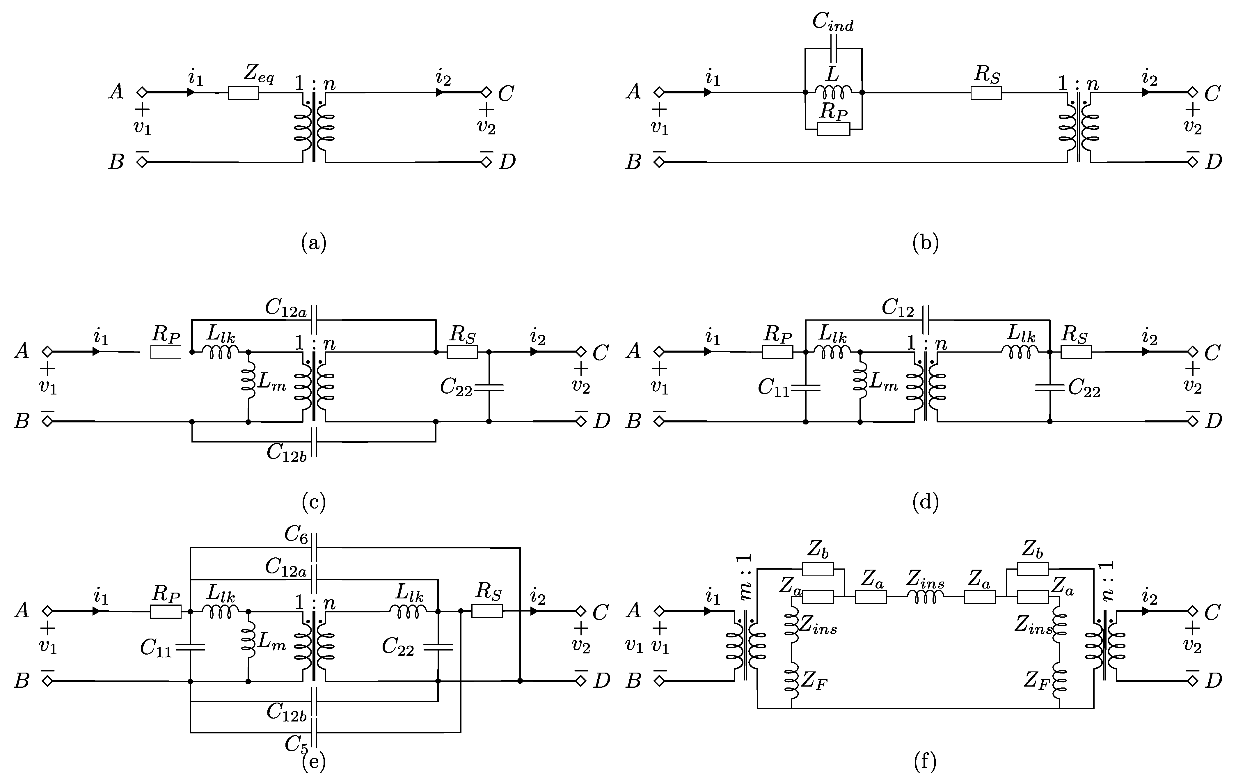
Figure 1. Transformer modeling overview. (a) Equivalent circuit with one equivalent AC resistance. (b) Equivalent circuit of the model proposed by [7][1]. (c) Equivalent circuit of the model proposed by [8][2]. (d) Equivalent circuit of the lumped model proposed by [9][3]. (e) Equivalent circuit of the six-capacitor model [10][4]. (f) Equivalent circuit of the lumped model proposed by [11][5].
In [8][2], an equivalent circuit with two interwinding capacitances and one intra-winding capacitance (shown in Figure 1c) was examined. In addition, the model uses winding resistances and inductances as well as a magnetization inductance. It was stated that this model is especially accurate if the transformer windings possess strong magnetic coupling [8][2]. This model requires fewer experiments to characterize compared to the traditional six-capacitor model. Using experimental evaluation, it has been demonstrated that this model can predict the behavior of the circuit over a wide range of frequencies. However, its prediction performance decreases as the operating frequency becomes too high.
A model with three parasitic capacitances, which is shown in Figure 1d, was proposed in [9][3]. This model also provides generally good accuracy for the examined operating frequencies.
An equivalent circuit with six parasitic capacitances was proposed in [10][4], as shown in Figure 1e. Using an energy-based approach, a model that uses six-parasitic capacitances was derived to describe the dynamic behavior of the model. While the six-capacitor model provides more accurate results compared to the lumped versions, it requires a higher number of tests and has a higher dynamic order. This leads to more complicated controllers and more computationally intensive simulations.
A different modeling approach was suggested by [11,12,13,14,15][5][6][7][8][9]. Contrary to the previous approaches, the authors obtained a circuit model by approximating the electromagnetic phenomena inside the transformer with a one-dimensional standing wave and solving the Maxwell equations for this case. The resulting equivalent circuit is shown in Figure 1f. It consists of a number of nonlinear impedances and, thus, is difficult to control. Furthermore, it can be seen that this model does not include parasitic capacitances. Compared to the experiment, the proposed model showed good performance, and each impedance has a direct physical interpretation. The parameters of the circuit model can be derived from the transformer datasheet using a one-dimensional wave propagation approach, as introduced in [11][5].
3. Parasitic Capacitance
With regard to different equivalent circuits for planar magnetics, numerous capacitances are present, and the behaviors of these capacitances should be deeply studied. This section discusses the parasitic capacitances that arise in planar magnetics. Initially, parasitic capacitances are discussed in terms of their types, where they occur within the circuits, and what mechanisms cause them. Following that, formulas and experiments are presented that can help estimate parasitic capacitances, as well as how to avoid them. Lastly, their effects on planar transformer-based converters and their interactions with other components are discussed.
In terms of electrical theory, a capacitor can be defined as any pair of conductive objects coupled together. Thus, numerous capacitances will be associated with magnetic devices between different parts of the device and with the surrounding environment. These capacitances are called parasitic capacitances and must be carefully considered during the design stage. At higher frequencies, a capacitor will behave more like a resistor on the verge of shorting out. Thus, parasitic capacitance poses a real problem at high frequencies, while it does not have a significant effect at lower frequencies [16][10]. With reference to Figure 2, parasitic capacitances can manifest themselves in the transformer in several ways, including (i) turn-to-turn capacitance between two turns in the same winding or different windings (CP−S), (ii) the capacitance between the windings and the magnetic cores (CP−C, CS−C), (iii) the capacitance between the windings/core and the ground (CC−G). The distribution is dependent heavily on the geometry and spatially distributed in nature [17][11].
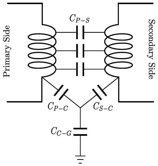
Figure 2. Parasitic capacitance sources in planar transformers. There are four kinds of parasitic capacitances in transformers. Parasitic capacitance between the primary and secondary (CP−S), which is between the windings. Parasitic capacitance between the primary side and the core (CP−C). Parasitic capacitance between the secondary side and the core (CS−C). Parasitic capacitance between the windings/core and the ground (CC−G).
Due to the considerable overlaps between the tracks in different layers of the windings of a planar transformer, there is a large parasitic capacitance between the layers of the primary winding and the secondary winding. The transformer is affected by an undesirable electrostatic coupling between the primary and secondary windings or between the windings and the core which is called common mode (CM) noise. A parasitic capacitance also results between the core and the layers of windings that are exposed to the core. Since the voltages of overlapping layers change rapidly as a result of high-frequency switching, the parasitic capacitances experience a high dv/dt value. The CM noise is the result of these oscillating currents that circulate through the circuit at high frequencies and causes EMI problems [18][12]. Previous studies [7,19][1][13] have developed analytical methods to estimate parasitic capacitance values in the design process. This model has also been used to design and optimize DC–DC isolated converters [20,21][14][15].
The design of planar transformers in LLC topologies has been the subject of several studies [22,23][16][17]. Topologies based on resonance studies suggest that the couplings between the oscillators and the transformer do not adversely affect gain or modulation when the power levels and frequencies are high. Whereas, in dual active bridge (DAB)-based topologies, they amplify the effect of the parasitics in the switches and can degrade the converter performance [24][18].
With the high-frequency operation, the parasitic capacitance in transformers and inductors has become an issue due to the fact that the impedance is affected considerably by parasitic capacitances. Thus, the operation frequency of these magnetics will be limited [24][18]. EMI and reduced efficiency are also caused by a high charge inrush current and high-frequency oscillations in the circuit [5][19]. It is also necessary to provide a reasonable amount of the switching current during the dead time in order to achieve zero-voltage switching for MOSFETs [25][20]. This causes parasitic capacitances to cause high-frequency current oscillations, so understanding how these oscillations occur is essential to minimizing parasitic effects in devices. It is, therefore, necessary to develop a parasitic capacitance model for planar magnetics in order to account for these effects.
In [24][18], guidelines for defining acceptable values for parasitic capacitances in transformers were provided, which matched the soft switching of a converter. Two examples were presented to illustrate the effects of winding geometries on transformer parameters. The first design used a PCB, and the thickness was minimized. The second design adjusted different leg heights to study different geometries. In both transformers, the inductances were minimized through interleaved windings to reduce losses. Layers were built parallel to the turns of the primary winding throughout the primary winding to reduce current density. The first transformer was designed to limit core and winding losses in the transformer without accounting for the constraint of interwinding capacitance. The second configuration was designed to optimize the trade-off between transformer losses and interwinding capacitance.
It is possible to estimate the parasitic capacitances in transformers of interleaved primary/secondary windings, with large copper conductors, using the classical plane capacitor equation [24][18]:
where geometric parameters that affect the capacitance include the number of parallel surfaces Nface, the surface area of each Sface, and the insulation spacing eFR4. ϵ0 is the permittivity and ϵr is the relative permittivity.
An electrostatic FEM model, to evaluate the parasitic capacitance of a two-turn transformer, was also carried out, which verifies the Cp value. The interwinding capacitance rises hyperbolically with the decreasing insulation thickness [24][18].
4. Leakage Inductance
The purpose of this section is to discuss leakage inductances in planar magnetics. Identifying their locations in the circuit and the mechanisms responsible for their occurrences is the first step. Following this, a set of formulas that can be used to estimate leakage inductances will be presented. Lastly, inductance is examined as a function of the distance between the layers and the core.
Leakage inductance is the imperfect coupling of the windings in the circuital model of a high-frequency transformer, and it represents an inductive element in the model [26][21], as can be seen in Figure 43. In [27][22], the leakage inductance of transformers is discussed in detail. The energy stored in the leakage inductance results in the generation of voltage spikes in the switches, which leads to lower efficiency and increased losses on the switches [28][23]. Energy in a low-leakage construction is mostly stored in the windings and the gaps between them. Moreover, the amount of stored energy in the leakage inductance is intrinsically independent of the core geometry and is mostly determined by the geometry of the windings themselves. There is, however, a particular difference in winding geometry caused by different core geometries that may impact the leakage inductance.
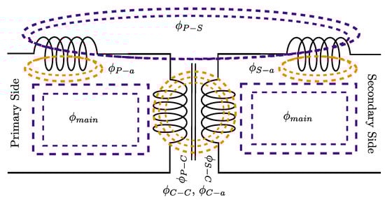
Figure 43. Flux leakage from core to air (ϕC−a), core to core (ϕC−C), primary winding to the core (ϕP−C), secondary winding to the core (ϕS−C), primary winding to air (ϕP−a), secondary winding to air (ϕS−a), primary winding to secondary winding (ϕP−S), and main flux (ϕmain).
Contrary to popular belief, the leakage inductance of a planar transformer is higher than that of a conventional transformer as an intrinsic property [29][24]. In [28][23], a comparison was conducted on the leakage inductance of a planar and a conventional structure, in which the leakage inductance of the planar structure is almost twice that of the conventional one. For the fairness of the experiment, the cross-section of the core, volume of the core, number of turns, and thickness of the conductors were kept the same. With increased core dimensions, the difference in leakage inductances between the two structures will increase. This is mainly due to the fact that the mean turn length (MTL) of planar magnetics is longer. Reference [29][24] compares the planar structure with other core structures, leading to the conclusion that planar structures do not have a low inductance by design; thus, the use of other methods, such as interleaving, should be considered to reduce the leakage inductance.
In addition, a planar winding with a higher aspect ratio of the conductor width to conductor thickness will naturally have a “radial effect”, which reduces leakage inductance [30][25]. There is a need to find accurate leakage inductance predictions for planar transformers since the winding width in a traditional transformer is much smaller than the winding height. Therefore, maximizing efficiency would require an optimized design. The leakage inductance for a nicely matched resonant frequency has also been investigated in planar transformers, such as LLC converters [31,32,33,34,35][26][27][28][29][30].
Research on the properties of planar transformers has focused on obtaining winding losses, largely using Dowell’s formula [36][31]. This formula may also be used to measure leakage inductance in conventional transformers. Accordingly, [37][32] proposed a novel set of formulas to calculate the self- and mutual inductances of a planar coil on a homogeneous ferromagnetic substrate. It should be noted that these formulas are not suitable for PCB windings with cores and are designed for air core planar windings and thick-film transformers.
As previously mentioned, a common misconception is that planar transformers have low leakage inductance intrinsically, compared to conventional counterparts. A planar transformer has an intrinsically longer MTL than a vertical structure [3][33]; leakage inductance is, therefore, increased. Dowell’s method has been extensively used in order to determine the leakage inductance of wire-wound transformers, whereas significant errors have been observed when applied to planar transformers. The main causes of these errors are as follows:
- 1.
-
Traditional analysis has only taken account of the leakage inductance at low frequency (frequency-independent), while high-frequency eddy currents have been ignored.
- 2.
-
The insulators between layers do not figure in traditional analytical expressions due to their small thickness. However, the copper thickness of a PCB winding (35–70 μm) is usually much smaller than its dielectric layer thickness, which is typically 200 μm. As a consequence of this, the analytical error can range up to ≈30%, or even higher [27][22], with regard to the layout dimensions.
- 3.
-
Conventional transformers were not affected by the “radial effect”.
The currents that are conducted along the inner edge of planar transformer windings concentrate towards the center of conductors. This affects the amplitude of the magnetic field adjacent to the center of the conductors. A novel analytical method was proposed in [30][25] for leakage inductances in planar transformers that combine all three factors discussed above, especially for “radial effects”. This approach separates the eddy current effect and the radial effect of leakage inductance by decomposing the leakage flux into longitudinal and transversal flux fields. With the proposed formula incorporating both high-frequency eddy current effects and radial effects, the accurate prediction of leakage inductance is available in transformers. Total leakage energy takes into account the stored energy from each elementary layer, which can be expressed using the following formula [30][25]:
where Ep, Es, and Ep are the energy stored in the primary winding, the energy stored in the secondary winding, and the energy stored in the dielectric layer, respectively. With the same layer thickness in every layer and defined turn, a total leakage inductance can be calculated by the following method:
where np and ns represent the number of turns in the primary and secondary. r1 and r2 are the distances between the center and the inner and outer edges of the core, respectively. hpℎ is equal to hsℎ, i.e., the thicknesses of the primary and secondary windings. hiℎ is the thickness of the dielectric. γ and μ0 are the propagation constant and permeability of air, respectively.
In [30][25], leakage inductance is compared between Dowell’s calculation [36][31] and a previous work presented in [38][34]. Along with the proposed calculation, an FEA simulation and experimental measurements are reported in the paper. The “radial effect” was neglected in the mentioned works, which led to over-estimations of the leakage inductance. Overall, the experimental measurement closely matches the proposed method.
Effect of PCB Layer Distance on Inductance
By changing the air gap lg, the magnetizing inductance of the transformer can be adjusted. This method uses two separate boards for the primary and secondary windings, providing an additional degree of freedom (lb). As a result, lb can be controlled to achieve precise leakage inductance values, which is a key design criterion for resonant converters. It is important to design the air gap length accurately to obtain the correct transformer parameters. The air gap length is calculated as follows: [1][35]:
where N is the number of primary side windings. Lm is the magnetizing inductance. le and Ae are the core’s effective length and area, respectively. μ0 and μr are the air permeability and relative permeability.
Having established the transformer parameters, the leakage inductance can then be determined by tuning lb. In order to calculate the lb, the length of the core’s leg, the air gap, and the thickness of the board must be taken into consideration.
5. Finite Element Analysis
Several different approaches have been introduced to model the behaviors of planar transformers. For electromagnetic analysis, FEA models [11,39,40,41,42,43,44,45,46,47,48][5][36][37][38][39][40][41][42][43][44][45] of the device provide accurate results compared to experiments [39,47][36][44] and reveal the detailed distributions of magnetic fields produced by the transformer. Another use of FEA is to obtain the parameters that are used in circuit models introduced in the previous section. In this way, it is possible to obtain the leakage inductance [44][41], or the entire impedance matrix [45][42] of the planar inductor. Due to the quasi-2D structure, the model can be reduced to a 2D one to reduce the computational complexity [40][37]. Moreover, a set of FEM models can be formulated for parameter variations and serve as the basis for the design and optimization of the transformer [42,43][39][40]. It is possible to extend the FEA to other physical domains in the FEA to obtain a more accurate picture of the situation. In [46][43], the authors built a numerical thermal model of a planar inductor based on FEA computations. When the behavior of the transformer with a core is of interest, the core can be included in the FEA. The core can be modeled as homogenous and the effects of lamination can be included by setting an anisotropic permeability [48][45]. Furthermore, the authors showed that any clamping can be neglected in the modeling without major decreases in accuracy. Even though FEA is an excellent tool, a 3D model is necessary for some arrangements, such as Litz structures, since 2D simulations cannot provide accurate results. A three-dimensional analysis of a planar magnetic device with a Litz structure faces two major challenges: the power and time required to simulate the model, as well as the requirement to provide accurate geometric representations of the structure [49][46].
References
- Shen, Z.; Wang, H.; Shen, Y.; Qin, Z.; Blaabjerg, F. An Improved Stray Capacitance Model for Inductors. IEEE Trans. Power Electron. 2019, 34, 11153–11170.
- Besri, A.; Chazal, H.; Keradec, J.P. Capacitive behavior of HF power transformers: Global approach to draw robust equivalent circuits and experimental characterization. In Proceedings of the 2009 IEEE Instrumentation and Measurement Technology Conference, Singapore, 5–7 May 2009; pp. 1262–1267.
- Lu, H.Y.; Zhu, J.G.; Hui, S.R. Experimental determination of stray capacitances in high frequency transformers. IEEE Trans. Power Electron. 2003, 18, 1105–1112.
- Duerbaum, T.; Sauerlaender, G. Energy based capacitance model for magnetic devices. In Proceedings of the APEC 2001. Sixteenth Annual IEEE Applied Power Electronics Conference and Exposition (Cat. No.01CH37181), Anaheim, CA, USA, 4–8 March 2001; Volume 1, pp. 109–115.
- Chen, M.; Araghchini, M.; Afridi, K.K.; Lang, J.H.; Sullivan, C.R.; Perreault, D.J. A Systematic Approach to Modeling Impedances and Current Distribution in Planar Magnetics. IEEE Trans. Power Electron. 2016, 31, 560–580.
- Tria, L.A.R.; Zhang, D.; Fletcher, J.E. High-Frequency Planar Transformer Parameter Estimation. IEEE Trans. Magn. 2015, 51, 8402604.
- Margueron, X.; Besri, A.; Lembeye, Y.; Keradec, J. Current Sharing Between Parallel Turns of a Planar Transformer: Prediction and Improvement Using a Circuit Simulation Software. IEEE Trans. Ind. Appl. 2010, 46, 1064–1071.
- Schellmanns, A.; Fouassier, P.; Keradec, J.; Schanen, J. Equivalent circuits for transformers based on one-dimensional propagation: Accounting for multilayer structure of windings and ferrite losses. IEEE Trans. Magn. 2000, 36, 3778–3784.
- Keradec, J.; Cogitore, B.; Blache, F. Power transfer in a two-winding transformer: From 1-D propagation to an equivalent circuit. IEEE Trans. Magn. 1996, 32, 274–280.
- Hutchinson, P.; Chaniotakis, P. Introduction to Electronics, Signals, and Measurement; Massachusetts Institute of Technology: Cambridge, MA, USA, 2004.
- Ghahfarokhi, N.S. Minimising Capacitive Couplings and Distributing Copper Losses in Planar Magnetic Elements. Ph.D. Thesis, Queensland University of Technology, Brisbane, Australia, 2010.
- Chu, Y.; Wang, S. A generalized common-mode current cancelation approach for power converters. IEEE Trans. Ind. Electron. 2015, 62, 4130–4140.
- Biela, J.; Kolar, J.W. Using transformer parasitics for resonant converters-A review of the calculation of the stray capacitance of transformers. In Proceedings of the Fourtieth IAS Annual Meeting. Conference Record of the 2005 Industry Applications Conference, Hong Kong, China, 2–6 October 2005; Volume 3, pp. 1868–1875.
- Saket, M.A.; Shafiei, N.; Ordonez, M. Planar transformer winding technique for reduced capacitance in LLC power converters. In Proceedings of the 2016 IEEE Energy Conversion Congress and Exposition (ECCE), Milwaukee, WI, USA, 18–22 September 2016; pp. 1–6.
- Magambo, J.S.N.T.; Bakri, R.; Margueron, X.; Le Moigne, P.; Mahe, A.; Guguen, S.; Bensalah, T. Planar magnetic components in more electric aircraft: Review of technology and key parameters for DC–DC power electronic converter. IEEE Trans. Transp. Electrif. 2017, 3, 831–842.
- Li, B.; Li, Q.; Lee, F.C. A novel PCB winding transformer with controllable leakage integration for a 6.6 kW 500 kHz high efficiency high density bi-directional on-board charger. In Proceedings of the 2017 IEEE Applied Power Electronics Conference and Exposition (APEC), Tampa, FL, USA, 26–30 March 2017; pp. 2917–2924.
- Chen, R.; Yu, S.Y. A high-efficiency high-power-density 1MHz LLC converter with GaN devices and integrated transformer. In Proceedings of the 2018 IEEE Applied Power Electronics Conference and Exposition (APEC), San Antonio, TX, USA, 4–8 March 2018; pp. 791–796.
- Demumieux, P.; Avino-Salvado, O.; Buttay, C.; Martin, C.; Sixdenier, F.; Joubert, C.; Magambo, J.S.N.T.; Löher, T. Design of a Low-Capacitance Planar Transformer for a 4 kW/500 kHz DAB Converter. In Proceedings of the 2019 IEEE Applied Power Electronics Conference and Exposition (APEC), Anaheim, CA, USA, 17–21 March 2019; pp. 2659–2666.
- Saket, M.A.; Shafiei, N.; Ordonez, M. LLC Converters With Planar Transformers: Issues and Mitigation. IEEE Trans. Power Electron. 2017, 32, 4524–4542.
- Everts, J.; Krismer, F.; Van den Keybus, J.; Driesen, J.; Kolar, J.W. Optimal ZVS modulation of single-phase single-stage bidirectional DAB AC–DC converters. IEEE Trans. Power Electron. 2013, 29, 3954–3970.
- Dang, Y.; Zhu, L.; Liu, J.; Zhan, C.; Long, L.; Ji, S. Module Integral Method for the Calculation of Frequency-Dependent Leakage Inductance of High-Frequency Transformers. IEEE Trans. Power Electron. 2022, 37, 7028–7038.
- Ouyang, Z.; Thomsen, O.C.; Andersen, M.A. The analysis and comparison of leakage inductance in different winding arrangements for planar transformer. In Proceedings of the 2009 International Conference on Power Electronics and Drive Systems (PEDS), Taipei, Taiwan, 2–5 November 2009; pp. 1143–1148.
- Ouyang, Z. Advances in Planar and Integrated Magnetics. Ph.D. Thesis, Technical University of Denmark (DTU), Lyngby, Denmark, 2011.
- Carsten, B. The low leakage inductance of planar transformers; fact or myth? In Proceedings of the APEC 2001. Sixteenth Annual IEEE Applied Power Electronics Conference and Exposition (Cat. No. 01CH37181), Anaheim, CA, USA, 4–8 March 2001; Volume 2, pp. 1184–1188.
- Ouyang, Z.; Hurley, W.G.; Andersen, M.A. Improved Analysis and Modeling of Leakage Inductance for Planar Transformers. IEEE J. Emerg. Sel. Top. Power Electron. 2018, 7, 2225–2231.
- Choi, J.M.; Byen, B.J.; Lee, Y.J.; Han, D.H.; Kho, H.S.; Choe, G.H. Design of leakage inductance in resonant dc-dc converter for electric vehicle charger. IEEE Trans. Magn. 2012, 48, 4417–4420.
- Biela, J.; Kolar, J.W. Electromagnetic integration of high power resonant circuits comprising high leakage inductance transformers. In Proceedings of the 2004 IEEE 35th Annual Power Electronics Specialists Conference (IEEE Cat. No. 04CH37551), Aachen, Germany, 20–25 June 2004; Volume 6, pp. 4537–4545.
- Huang, D.; Ji, S.; Lee, F.C. LLC resonant converter with matrix transformer. IEEE Trans. Power Electron. 2013, 29, 4339–4347.
- Xu, X.; Khambadkone, A.M.; Leong, T.M.; Oruganti, R. A 1-MHz zero-voltage-switching asymmetrical half-bridge DC/DC converter: Analysis and design. IEEE Trans. Power Electron. 2006, 21, 105–113.
- Jung, J.H. Bifilar winding of a center-tapped transformer including integrated resonant inductance for LLC resonant converters. IEEE Trans. Power Electron. 2012, 28, 615–620.
- Dowell, P. Effects of eddy currents in transformer windings. In Proceedings of the Institution of Electrical Engineers; IET: Stevenage, UK, 1966; Volume 113, pp. 1387–1394.
- Hurley, W.G.; Duffy, M.C. Calculation of self and mutual impedances in planar magnetic structures. IEEE Trans. Magn. 1995, 31, 2416–2422.
- Ouyang, Z.; Andersen, M.A.E. Overview of Planar Magnetic Technology—Fundamental Properties. IEEE Trans. Power Electron. 2014, 29, 4888–4900.
- Ouyang, Z.; Zhang, J.; Hurley, W.G. Calculation of leakage inductance for high-frequency transformers. IEEE Trans. Power Electron. 2014, 30, 5769–5775.
- He, P.; Mallik, A.; Sankar, A.; Khaligh, A. Design of a 1-MHz High-Efficiency High-Power-Density Bidirectional GaN-Based CLLC Converter for Electric Vehicles. IEEE Trans. Veh. Technol. 2019, 68, 213–223.
- Djuric, S.; Stojanovic, G.; Damnjanovic, M.; Radovanovic, M.; Laboure, E. Design, Modeling, and Analysis of a Compact Planar Transformer. IEEE Trans. Magn. 2012, 48, 4135–4138.
- Aime, J.; Cogitore, B.; Meunier, G.; Clavel, E.; Maréchal, Y. Numerical Methods for Eddy Currents Modeling of Planar Transformers. IEEE Trans. Magn. 2011, 47, 1014–1017.
- Taylor, L.; Margueron, X.; Le Menach, Y.; Le Moigne, P. Numerical modelling of PCB planar inductors: Impact of 3D modelling on high-frequency copper loss evaluation. IET Power Electron. 2017, 10, 1966–1974.
- Cove, S.R.; Ordonez, M.; Luchino, F.; Quaicoe, J.E. Applying Response Surface Methodology to Small Planar Transformer Winding Design. IEEE Trans. Ind. Electron. 2013, 60, 483–493.
- Deng, J.; Li, W.; Nguyen, T.D.; Li, S.; Mi, C.C. Compact and Efficient Bipolar Coupler for Wireless Power Chargers: Design and Analysis. IEEE Trans. Power Electron. 2015, 30, 6130–6140.
- Zhang, J.; Ouyang, Z.; Duffy, M.C.; Andersen, M.A.E.; Hurley, W.G. Leakage Inductance Calculation for Planar Transformers With a Magnetic Shunt. IEEE Trans. Ind. Appl. 2014, 50, 4107–4112.
- Zhang, X.; Ho, S.L.; Fu, W.N. Quantitative Analysis of a Wireless Power Transfer Cell With Planar Spiral Structures. IEEE Trans. Magn. 2011, 47, 3200–3203.
- Wrobel, R.; McNeill, N.; Mellor, P.H. Performance Analysis and Thermal Modeling of a High-Energy-Density Prebiased Inductor. IEEE Trans. Ind. Electron. 2010, 57, 201–208.
- Mu, M.; Zheng, F.; Li, Q.; Lee, F.C. Finite Element Analysis of Inductor Core Loss Under DC Bias Conditions. IEEE Trans. Power Electron. 2013, 28, 4414–4421.
- Jurković, Z.; Jurišić, B.; Župan, T. Fast Hybrid Approach for Calculation of Losses in Outer Packages of Transformer Core Due to Perpendicular Stray Flux. IEEE Trans. Magn. 2021, 57, 8401504.
- Kolahian, P.; Tazehkand, M.Z.; Baghdadi, M. Design and Assessment of Track Structures in High-Frequency Planar Inductors. TechRxiv, 2022; preprint.
More