1. Chemical Reactions of CWAs and Their Simulants Used in MOS Sensors
The available literature on metal oxide semiconductors (MOS) sensors is dominated by works describing the detection of simulants of nerve and blister chemical warfare agents (CWAs). At the same time, there are some papers on the detection of simulants of blood and choking agents. In addition, individual articles describing the detection of actual CWAs can be found
[1][2].
Most of the studies on the detection of nerve CWAs have been conducted with the use of dimethyl methylphosphonate (DMMP), which is a commonly used sarin simulant. The mechanism of the DMMP reaction on the surface of a semiconductor sensor has been studied many times and is well described in the literature
[3][4][5][6].
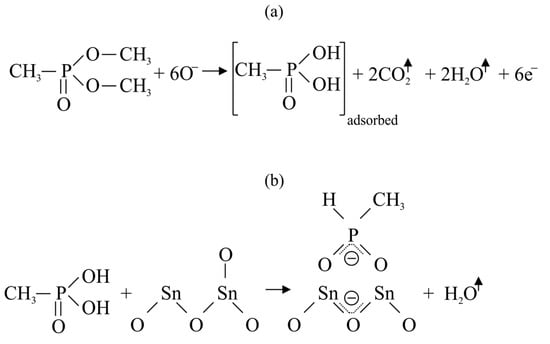
Figure 1 shows the reaction of DMMP with oxygen anions taking place on the surface of SnO
2 according to a generally accepted mechanism
[4].
Figure 1. Oxidation of DMMP molecule on the SnO2: (a) reaction between SnO2 and DMMP; (b) reaction between methylphosphonic acid and SnO2 resulting in adsorption of phosphorus compounds on the oxide surface.
At a temperature ranging from 300 to 600 °C, DMMP reacts with Oˉ ions, which leads to the release of electrons into the semiconductor and changes in the resistance of the sensor. In the case of DMMP detection, the phenomenon of sensor poisoning is often observed, manifested by prolonged signal recovery and even a permanent decrease in sensor sensitivity. This phenomenon is explained by the fact that the oxidized form of DMMP (methylphosphonic acid) is permanently adsorbed on the surface of the semiconductor (in this case, SnO
2 (
Figure 1b), but the poisoning effect is also observed for ZnO
[7], Mn
3O
4 [8] and many other materials). As a result, the active surface of the semiconductor available for oxygen ionosorption and reaction with DMMP decreases. The problem of sensor poisoning also occurs with other organophosphate simulants, such as diethyl methylphosphonate (DEMP)
[9].
In the case of blister agent detection, numerous tests were carried out with the simulants of sulfur mustard-2-chloroethyl ethyl sulfide (2-CEES) and with the simulant of nitrogen mustard-di(propylene glycol)monomethyl ether (DPGME). There is also work describing research with actual sulfur mustard
[1]. In addition, some papers contain studies on the detection of blood and choking agent simulants (primarily dichloromethane-DCM—a simulant of phosgene, and acetonitrile-ACN—a simulant of hydrogen cyanide).
The mechanisms underlying the detection of all these compounds in MOS sensors are very similar. In each case, the analyte is oxidized with the formation of simple gaseous products such as CO
2, H
2O, NO
2, Cl
2 or SO
2, which do not cause contamination of the sensor surface (the exception is the detection of DCM, which significantly poisons the SnO
2 sensor
[10][11] and dichloropentane (DCP)
[1]). An example of this type of reaction is the oxidation of 2-CEES on the surface of CdSnO
3 [12]:
At 300 °C, the 2-CEES molecule breaks down into radicals on the surface of the semiconductor. These radicals then react with adsorbed oxygen ions to release electrons. In this case, the sensor poisoning effect was not observed
[12][13][14]. It is also worth noting that in the available literature, there are papers that present in detail the mechanism of ACN detection
[15][16][17].
Historically, the first paper in which MOS sensors (SnO
2, ZnO) were used to detect vapors of organophosphorus compounds was published in 1993
[18]. Over the years, intensive research in this field has resulted in a number of significant achievements, including improvements in the sensitivity, selectivity and stability of sensors. The review of the subjectively most important achievements in the field of MOS sensors in CWAs detection was based on the criterion of the semiconductor material used, separating materials based on SnO
2, ZnO and other semiconductor oxides.
2. Sensors Based on SnO2
The first generation of semiconductor materials used in the detection of chemical warfare agents and their simulants were polycrystalline (also nanocrystalline) powders, mainly SnO
2. These materials were usually used in the form of thick layers (films) applied to the sensor surface by screen printing or in the form of pressed disks
[10][11][19][20][21][22][23]. In addition to sensors with thick layers (typically 1 to 300 μm thick), sensors with polycrystalline films classified in the literature as thin layers (up to about 1 μm thick) were also used. Thin layers were most often produced by the rheotaxial growth and thermal oxidation (RGTO) method
[24][25].
Paper
[10] describes the results of testing both undoped and doped SnO
2 thick film sensors used for DMMP, DPGME, ACN and DCM detection. In this study, SnO
2 sensors differing in grain size (40 and 15 nm) and applied dopants (Co
3O
4, Nb
2O
5, MoO
3, NiO, Sb
2O
3) were used. The sensors were operated at 350 °C and exposed to a gas stream with concentrations of simulants ranging from 0.02 to 0.8 ppm. The presented results showed the influence of the grain size, porosity of the semiconductor layer and the type of dopant used on the sensitivity, selectivity and dynamic parameters of the sensors. It was found that dopants significantly affect the sensitivity of the sensor. An example may be a sensor with SnO
2 doped with NiO, for which the response to DPGME, DMMP, DCM vapors increased by 24, 38 and 1300%, respectively, compared to the undoped sensor. Significant observations also concerned the recovery time of the sensors. In the case of DMMP and DCM detection using undoped SnO
2 sensors, prolonged recovery times and a decrease in sensor sensitivity were observed. These phenomena were attributed to the poisoning of the sensor surface with the products of analyte oxidation. The magnitude of the poisoning effect was significantly reduced in the case of the MoO
3-doped sensor.
The issue of optimizing the content and composition of dopants towards eliminating the poisoning effect was developed by the same research team in subsequent works
[11][19]. In work
[19], a sensor equipped with a thick SnO
2 layer doped simultaneously with NiO, MoO
3 and Sb
2O
3 was developed, which reportedly showed no poisoning effect during DMMP detection. The influence of individual dopants on the properties of the sensor was empirically identified: the addition of NiO improved the signal amplitude, while MoO
3 and Sb
2O
3 shortened the sensor recovery time. Similarly, work
[11] describes a completely reversible SnO
2 sensor for detecting DCM. In this case, the participation of NiO in the improvement of the response to DCM and MoO
3 and in the reduction of recovery time was also found.
Further studies, aimed at improving the dynamic parameters of SnO
2 sensors during DMMP detection are described in
[26]. The authors of the cited paper manufactured sensors with thick polycrystalline films made of undoped and doped SnO
2 nanoparticles. SnO
2 nanoparticles were obtained by the hydrothermal method and had a diameter of approximately 10 nm. Ni, Sb and Nb were used as dopants. As a reference, the sensor with a commercially available SnO
2 nanopowder (with an estimated grain size of several tens of nanometers) was used. The results revealed that the sensors with synthesized, undoped SnO
2 had a much higher sensitivity to DMMP than the sensor with commercial powder (72 vs. 3.1, respectively, for a DMMP concentration of 5 ppm). The increase in sensitivity was attributed to the larger specific surface area of the nanoparticles. At the same time, the sensors with synthesized SnO
2 returned to equilibrium much slower after switching off the DMMP. Doping with metals significantly shortened the response and recovery times. Particularly good results were achieved for sensors doped with 5% wt. Ni. As reported by the authors, this sensor was characterized by a complete signal recovery in less than 10 min after the DMMP was turned off. At the same time, doping SnO
2 with Ni significantly reduced the sensitivity of the sensor.
In
[20], thick-film SnO
2 sensors were also studied. In the cited publication, they were used to detect CWAs simulants such as DPGME, DMMP, DCM and ACN. The research was aimed at investigating the influence of the porosity of the semiconductor layer on the sensitivity toward individual analytes. For this purpose, sensors with four different SnO
2 materials, characterized by different specific surface areas and pore size distribution, were prepared. The results showed that the sensitivity of the sensor is influenced not only by the total specific surface area of the semiconductor layer, but also by the pore size distribution of the layer. For this reason, the sensitivity towards individual analytes differing in mass and molar volume does not increase monotonically with the increase in specific surface area. Research showed that sensors with larger pore sizes were more sensitive to larger molecules (DMMP and DCP). At the same time, materials with a higher specific surface area, but available mainly in micropores, showed lower sensitivity towards these substances.
Sensors with a porous SnO
2 film were also investigated in
[2]. In this case, a sensor with an ethanol-aged, nanoporous thin film of undoped SnO
2 was presented, which was used to detect real sarin gas (GB). The use of controlled ethanol aging (exposure to 100 ppm ethanol vapor in air at 300 °C for 12 h) significantly changed the performance of the sensor during GB detection. The sensor at a temperature of 300 °C showed unusual behavior for a sensor with an n-type semiconductor in the presence of reducing GB. As a result of the sorption of this gas, the resistance increased as in the case of oxidizing gases. At the same time, the effect was not observed with DMMP. Additionally, at 400 °C, the anomalous behavior towards GB was no longer observed. The authors explain this phenomenon by the adsorption of -CH
x groups on the SnO
2 surface as a result of previous exposure to ethanol. During the detection of GB, the fluorine atom present in GB captures electrons from the -CH
x groups and, thus, also from the semiconductor layer, causing an oxidative response of the sensor (increase in resistance). Parallel to this process, GB is oxidized by interaction with Oˉ, and electrons are released into the semiconductor. However, the result of these processes is an increase in the resistance of the sensor. As research has shown, the sensor can detect GB at a very low concentration of 6 ppb and distinguish GB from DMMP.
Noteworthy is also the interesting design solution of the sensor used in
[2], which allows for a significant reduction in electricity consumption. The device was made with MEMS technology. Its active part was made of a SiO
2/Si
3N
4 in the form of a square-shaped membrane with a side of 150 μm and a thickness of 1 μm. The membrane, which was integrated with the heater and platinum IDEs, was suspended over the bulk silicon slice via four slender cantilever beams. A film with SnO
2 was then applied to the membrane surface by the sacrificial template method. In the case of this method, the semiconductor layer is produced using a template (e.g., polystyrene), thanks to which it was possible to deposit a highly ordered monolayer of SnO
2 nanospheres from a liquid solution (the template itself is burned away in the process of annealing the film). The produced sensor was characterized by a significantly reduced power consumption (25 mW at 350 °C compared to typical 100–300 mW
[27]). A detailed description of the manufactured device is included in
[28].
A very problematic issue in the case of MOS sensors is the relatively low selectivity resulting from the fact that their principle of operation is based on rather non-specific oxidation and reduction reactions taking place on the grain surface. One of the ways to improve selectivity is the use of appropriately selected dopants. In the case of sensors with SnO
2 as the basic semiconductor material, the following dopants were most often used: Pt, Pd
[15][21], ZnO, ZrO
2, Al
2O
3, In
2O
3 [21], CuO, Sm
2O
3 [22], Co
3O
4, Nb
2O
5, MoO
3, NiO, Sb
2O
3 [10]. In most of the published works, the selection of dopants was carried out empirically rather than on the basis of general principles resulting from the mechanisms of the influence of individual dopants on the sensor’s selectivity. One such work is publication
[21], which describes a series of thick-film sensors based on SnO
2 doped with different contents of metals (Pt, Pd) or metal oxides (Al
2O
3, In
2O
3, ZnO, ZrO
2). Semiconductor materials were prepared by methods such as impregnation (Pt, Pd), physical milling (Al
2O
3, In
2O
3) or co-precipitation (ZnO, ZrO
2). Sensors prepared by screen printing were tested in the presence of DMMP, DPGME, DCM and ACN. As the research showed, the addition of sensitizers significantly influenced the sensitivity of the sensors to individual substances. From among the prepared sensors, four characterized by good sensitivity and stability were selected and used in a sensor array. The analysis of the four-dimensional signal was based on the principal components analysis. As the results showed, the array successfully distinguished vapors of individual simulants.
Another work aimed at improving the selectivity of MOS sensors is
[23]. The paper presents an array consisting of 15 commercial MOS sensors (manufactured by Figaro
[27]) with polycrystalline SnO
2 thick films. In the manufacturer’s catalog, individual sensors are described as intended for detecting various organic solvents and gases, but not as targeting CWAs. The intention of the authors was, therefore, to create an array of sensors for CWA detection that meets the definition of a dual-use device. The ability to selectively detect CWAs was to be ensured by using a relatively large number of different MOS sensors and using statistical analysis to interpret the multidimensional signal of the array. In the work, measurements were carried out with nerve CWA simulants such as diethyl diethyl cyanophosphate (DCNP), diisopropyl fluoride, chlorophosphonate and their derivatives, as well as some interferents. As the results showed, the array distinguished individual organophosphorus analytes. In addition, on the basis of the signal, a quantitative analysis was possible (calibration was performed against DCNP only, limit of detection (LOD) of 5 ppm was obtained). Despite the fact that the authors of the study found that the array may be suitable for detecting actual CWA in the field, the LOD values obtained for DCNP significantly exceed the immediate dangers to life or health (IDLH) values of nerve agents
[29]. Noteworthy, however, is the good selectivity of the array.
The use of polycrystalline sensor layers, especially those made of coarse grains, is associated with certain limitations. Larger grains are characterized by a lower surface to volume ratio, which limits the active surface on which redox reactions with analyte molecules can take place. Moreover, in the case of such grains, the depletion in charge carriers usually concerns only the surface layer of the grain (regional depletion), and not its entire volume. This results in less change in the conductivity of the layer due to depletion. For this reason, numerous research works focus on the use of semiconductor materials in the form of nanostructures such as: nanostrips, nanowires or nanotubes
[24][25][30][31][32]. In the case of nanostructures, it is possible to achieve lateral dimensions comparable to the depth of the charge carrier depletion area. Such materials will, therefore, show volume depletion, and thus, the processes occurring on their surface will strongly affect the conductivity of the semiconductor film. In addition, the peculiar structure of the nanomaterials is characterized by a larger specific surface area. It is also worth noting that the use of single (or parallel) monocrystalline nanostrips or nanowires opens up new perspectives in the field of MOS sensors, consisting of the production of sensors without grain boundaries. Sensors of this type could be characterized by a number of desirable features, such as the lack of long-term drift associated with the reorganization of grain boundaries (grain coarsening) under the influence of high temperatures
[33] or reducing the poisoning effect
[32].
The work
[24] presents a comparative study of MOS sensors equipped with SnO
2 and In
2O
3 nanowires and sensors equipped with traditional polycrystalline oxide layers. Semiconductor nanowires were fabricated using the vapor–liquid–solid (VLS) method. In this method, semiconductor powders are thermally evaporated and then absorbed to a supersaturated concentration in droplets of a catalytic liquid platinum alloy deposited on a sensor substrate. By maintaining appropriate thermodynamic conditions, the growth of single-crystalline nanowires is obtained in accordance with a specific crystallographic direction at the substrate–liquid alloy interface. In the cited paper, sensor responses to vapors of DMMP, DPGME, ACN and other substances (NH
3, acetone, ethanol and CO) were tested. Research has revealed a higher sensitivity of sensors with nanowires than with traditional films to DMMP and DPGME vapors (allowing their detection at concentrations close to 100 ppb). At the same time, lower sensitivity to other gases, such as NH
3 and CO, was observed. For all sensors, a strong signal drift was observed, indicating the occurrence of the poisoning effect. The sensor responses were also statistically analyzed to determine their suitability to the sensor array. The authors found that due to significant differences in sensitivity to individual substances, it is advisable to use both sensors equipped with nanowires and traditional polycrystalline films in the array.
A continuation of the above research was presented in
[25]. In this case, sensors with nanowires and polycrystalline SnO
2 films were also compared. The research focused on the qualitative and quantitative description of the sensor poisoning effect by phosphorus compounds during DMMP detection. Research includes testing sensor response to ethanol (25 ppm) and DMMP (0.2 ppm) vapors. The sensors were exposed alternately to these two gases to examine the degree of signal reduction from ethanol under the influence of DMMP poisoning. Studies have shown that the poisoning effect occurs on a similar scale for both types of semiconductor layers. The authors found that the drift of the sensor response in the short term is mainly caused by the contamination of the surface with phosphorus compounds. After a longer period of time without exposure to DMMP (in this work, it was 6 days at 400–500 °C), however, these compounds desorb, and full recovery of the sensor response was possible.
The use of sensors with SnO
2 nanowires for the detection of DMMP and ACN has also been described in
[31]. The study deepened the analysis of sensor poisoning under the influence of DMMP. Research has confirmed that initially, the sensitivity of the sensor decreases rapidly under the influence of repeated exposures to this gas. However, it was found that after long-term exposure (when the product of concentration and time reached approximately 800 ppm·min), the sensor’s response to DMMP stabilized, although the sensitivity was reduced by about 20 times. The effect of sensor poisoning on the detection of ethanol vapors (alternating exposure of the sensor to ethanol and DMMP vapors) was also studied. In this case, it was noted that despite the stabilization of the response to DMMP, subsequent exposures to this gas reduced the response to ethanol, which indicated progressive poisoning. Reduction of sensitivity to ethanol, and probably also to other reducing gases, may have an impact when the sensor is used in an array to distinguish CWAs from interfering gases.
Interesting research results are also presented in
[32], which describes a DMMP sensor using a single, monocrystalline, undoped SnO
2 nanobelt. The aim of the authors was to create a sensor free of grain boundaries. Tests conducted at 500 °C showed that the sensor relative signal reached 5 and 3% at 78 and 53 ppb of DMMP, respectively. Additionally, the authors did not observe the poisoning effect commonly seen with polycrystalline sensors. Noteworthy is the interesting design solution of the sensor setup. To ensure good thermal insulation, a system consisting of a single SnO
2 nanobelt and a heater (which was also a temperature sensor) was suspended in gas on silicon nitride fibers. Thanks to this, it was possible to significantly reduce the energy consumption of the sensor.
In the recently published work
[34], a sensor with oxygen vacancy-enriched SnO
2 decorated with Au nanoparticles was presented. Modification of commercial SnO
2 consisted of reaction with (CH
3)
2SnCl
2 and then calcination in air atmosphere. As a result, a significant increase in the concentration of oxygen vacancies on the semiconductor surface was obtained (increase of about 30%; the SnO
2 modification process was described in detail in
[35]). Au nanoparticles in the amount of 5% wt. Au were then deposited on the modified SnO
2 layer using the in situ reduction method (using HAuCl
4 aqueous solutions). The sensor prepared in this way was used to detect DMMP. The sensor obtained a relative signal of about 19% at a DMMP concentration of 240 ppb at 320 °C. The detection limit was estimated at 4.8 ppb. The sensor was also characterized by above-average dynamic parameters with response and complete recovery times of 26 and 32 s, respectively. Such good sensor properties were attributed by the authors of the cited paper to the total effect of three mechanisms: increasing the number of oxygen vacancies by modifying the surface with (CH
3)SnCl
2, creating metal-semiconductor junctions and thus better modulating the conductivity of the layer and the catalytic effect of Au nanoparticles. The sensor testing results presented in the cited paper are among the best obtained so far for SnO
2 sensors. It is noteworthy that, in this case, at the optimum operating temperature (320 °C), no poisoning was found, and the sensor was completely reversible.
3. Sensors Based on ZnO
ZnO is also often used in MOS sensors to detect CWA simulants
[7][14][36][37][38]. The advantages of this material include non-toxicity, abundance in the environment and stability. Similar to SnO
2, ZnO is an n-type semiconductor.
In
[39], a sensor with nanocrystalline ZnO powder modified with platinum (0.12% at.) was described. The sensor material was synthesized using the ultrasonic atomization technique and then applied to the substrates by screen printing to form thick films. Platinum was introduced by dipping pure ZnO films into an aqueous solution of chloroplatinic acid and annealing at a high temperature (500 °C). Sensors prepared in this way were tested for DMMP, 2-CEES and 2-chloroethyl phenyl sulfide (CEPS, sulfur mustard simulant). Studies have shown that the sensor with the optimal content of Pt (0.12% at.) was very sensitive and selective towards DMMP (the response to 2 ppm DMMP in 300 °C was about 9 and 26 times higher, respectively, than to 2-CEES and CEPS. Moreover, the sensor showed very good dynamic properties with DMMP response and recovery times of 15 and 45 s, respectively. There was also no sensor poisoning observed with alternating exposure to 2 ppm DMMP.
The work
[36] presents the sensor with a polycrystalline ZnO film. Undoped nanoparticles were obtained by the hydrothermal method and had diameters in the range of 30–50 nm. The sensor was used for the detection of 2-CEES and allowed to obtain a relative signal of 15 for a 2-CEES concentration of 1 ppm (estimated LOD of this compound was 0.2 ppm).
In subsequent work published by the same scientific group
[14], it was demonstrated that a significant improvement in the sensitivity of ZnO sensors is possible by appropriate doping of the semiconductor material. In the work, sensors doped with the following metals were tested: Al, Co, Cu and Mn. As research has shown, doping with Al significantly improves the sensitivity towards 2-CEES. For the sensor with optimal Al content (1% at.) at 500 °C and for an analyte concentration of 20 ppm, a relative signal of 954.2 was obtained (which is approximately 10 times more than for undoped sensor). In addition, the doped sensor was highly selective toward 2-CEES (the sensor responses obtained for 10 ppm NH
3, CO and NO were 0.73, 0.14 and 0.11, respectively). As stated by the authors, Al doping increases the concentration of oxygen vacancies on the ZnO surface. As a reason for observing a strong amplification only in the case of Al, the authors indicate a different electron configuration of this element with three valence electrons (in contrast to other used metals). Nevertheless, the work does not provide a detailed explanation and deeper analysis of this issue.
The issue of Al-doped ZnO was continued in
[37]. This paper describes a miniature GC system with an MOS detector for the detection of 2-CEES in mixtures. The MOS sensor was equipped with a film of 5 nm ZnO Quantum Dots doped with 1% at Al. The chromatograph used a 5 cm (0.15 cm diameter) packed column with Carbowax 20 M. The column was kept at 30 °C during analysis. Atmospheric air was used as the carrier gas, which was sucked into the system by means of a built-in pump. The sensor acted as a detector at a temperature of 430 °C. The detectability of 2-CEES was 0.5 ppm. Under optimal operating conditions, the retention time of 2-CEED was 150 s. The use of the column enabled the complete separation of CO, NO and NH
3, which thus did not interfere with the detection of 2-CEES. The intention of the authors was to significantly improve the selectivity of MOS sensors through the use of a combined technique. As the results of the analyses showed, the device was indeed characterized by above-average selectivity, at the cost of a significant complexity of construction. It is also worth paying attention to the parameters of the sensor produced as a detector in the GC system. The sensor was characterized by much higher sensitivity than the previously described solutions. In the case of 20 ppm 2-CEES at 450 °C, a relative signal of 5395 was obtained. The outstanding sensitivity was attributed to the effect of the size of the synthesized nanoparticles (under analogous conditions, a sensor with larger nanoparticles of doped ZnO achieved a signal of 673).
A significant achievement in the field of semiconductor sensors for DMMP detection is described in
[38]. The authors fabricated a sensor with a polycrystalline ZnO (average grain diameter of 25 nm) doped with 1% wt. Al. The nanoparticles were produced by the hydrothermal method. Tests have shown that the sensor was characterized by high sensitivity toward DMMP and low LOD. At the optimal operating temperature (350 °C), a relative signal of 4347 was obtained for the DMMP concentration of 10 ppm. At the same time, the estimated LOD of this substance was 100 ppb. The dynamic properties of this sensor are also noteworthy. With a response time of 2 s and a full recovery time of 96 s, it is probably the fastest MOS DMMP sensor reported in the literature. The sensor was also characterized by high selectivity to DMMP. The outstanding properties of the sensor reported in the cited paper were attributed by the authors to an increase in the concentration of oxygen vacancies in doped ZnO. Al
3+ ions replace Zn
2+ ions in the crystal lattice of the semiconductor. Due to the smaller ionic size, Al dopants can generate more oxygen vacancies and act as preferential adsorption sites for DMMP.
One of the ways to improve the sensitivity of MOS sensors is the use of dopants that form semiconductor junctions or metal–semiconductor junctions with the base semiconductor. When two different semiconductors come into intimate contact, due to the differences in the Fermi levels of both materials, energy bands will bend at the contact surface and a potential barrier (Schottky barrier) will be created. Changes in the concentration of charge carriers caused by the redox reaction, taking place on the surface of the semiconductor, affect the height of the created barrier and, thus, also the conductivity of the material. Changes in the conductivity of the layer in the case of an n-p heterojunction are proportional to the height of the potential barrier as follows
[40]:
where: k
B—Boltzmann constant, ΔΦ
B—change in height of Schottky barrier, T—temperature.
Particularly interesting results for a system of this type have been described in
[7]. In this case, a material based on ZnO nanostructures (called by authors “micron-scale ZnO flowers”) decorated with CuO nanoparticles was presented. In the cited paper, the responses of sensors with CuO/ZnO nanostructures and pristine ZnO nanostructures to DMMP were compared. During the measurements, it was revealed that the CuO/ZnO sensor is characterized by a much higher sensitivity to DMMP than the ZnO sensor and good selectivity towards this substance (the value of the relative signal for 10 ppm DMMP at 350 °C was 626.21, and for the same concentration of NH
3, CO, NO and NO
2 values of relative signals did not exceed 50). In addition, the response time of the CuO/ZnO sensor to DMMP was almost 13 times shorter than that of the ZnO sensor (26.2 and 330 s, respectively). The studies have shown that the addition of CuO causes a significant increase in sensor resistance in clean air, which may be caused by the expansion of the EDL by the formation of p-n junctions. At the same time, during exposure to DMMP, the width of the depletion area is reduced, and the resistance decreases to a value close to the value achieved by a sensor with pristine ZnO under the same conditions. As a result, the modulation of the sensor signal is four times wider than in the case of a sensor with pristine ZnO. A detailed analysis of the results contained in the cited publication also allows us to draw conclusions about the short-term repeatability of the sensors. It is clear that the sensors show a decrease in the sensitivity to DMMP during subsequent, repeated exposure cycles. This phenomenon has already been mentioned for SnO
2 sensors and results from the poisoning of the sensor surface with phosphorus compounds.
4. Sensors Based on Other Semiconductor Oxides
In addition to SnO
2 and ZnO-based materials, other oxides were also used in MOS sensors for the detection of CWAs and their simulants. These include materials such as: WO
3, In
2O
3, CuO
[1][24][41], MnO
2, Mn
3O
4 [8][42][43][44] or CdSnO
3 [12][14].
The work
[1] presents thick film sensors with undoped WO
3 and In
2O
3 used for the detection of actual CWAs and their simulants. The list of analytes included sarin, soman (GD), sulfur mustard (HD) and simulants (DMMP, DCP—dichloropentane). Both tested sensors showed high sensitivity to CWAs and estimated GB and HD detection limits of 10 ppb at 400 °C. In addition, the sensors were found to be much more sensitive to live agents than to their simulants. An interesting observation was the trend of increasing the sensitivity of the WO
3 sensor in the group of organophosphorus compounds: DMMP-GB-GD. This phenomenon was attributed to the increase in the number of methyl groups in the analyte molecule. During adsorption of the analyte, these groups are oxidized and constitute a source of additional electrons. As in the case of DMMP for GB and GD, the sensors showed poisoning.
In
[12], sensors with thin films of polycrystalline CdSnO
3 and Pt-doped CdSnO
3 are described. Several sensors with different thicknesses of semiconductor films were manufactured and tested. As determined by X-ray diffraction, CdSnO
3 grains were characterized by an average diameter of less than 5 nm. The films were deposited using the ultrasonic spray pyrolysis technique. The manufactured sensors were used to detect sulfur mustard simulants: 2-CEES and CEPS, as well as a sarin simulant-DMMP. The study revealed that both undoped and platinum-doped sensors were highly sensitive and selective towards 2-CEES. In the case of the undoped sensor (with a film thickness of 1.87 μm) at 350 °C, the signals for 4 ppm 2-CEES, CEPS and DMMP were: 12.05, 2.04 and 2.14, respectively. Under the same conditions at 250 °C, the signals for the Pt-doped sensor (1% vol., film thickness 1.14 μm) reached 58.63, 6 and 3.85. As the results showed, Pt doping significantly increased the sensitivity to 2-CEES and lowered the optimal operating temperature of the sensor from 300 to 250 °C. In addition, as the authors indicate, the dynamic parameters of the sensor have improved.
Further work on CdSnO
3 sensors focused on Ru doping
[13]. In this case, as before, the films were produced using the ultrasonic spray pyrolysis technique. Several sensors differing in the percentage content of ruthenium and the thickness of the polycrystalline films were manufactured and tested in the work. 2-CEES, CEPS and DMMP were used in the study. The best results were obtained for a sensor with a Ru content of 1.85% wt. and a film thickness of 365 nm. This sensor was characterized by a relative response to 2-CEES, CEPS and DMMP of 62.12, 7.23 and 4.9, respectively, at 350 °C. By comparing these results to those previously obtained for undoped CdSnO
3 and platinum-doped CdSnO
3 [12], it can be concluded that metal-doped sensors are characterized by similar sensitivity and selectivity towards 2-CEES. In the case of the Ru-CdSnO
3 sensor, a much shorter response and recovery time was obtained (for 4 ppm 2-CEES: 5 and 185 s, respectively). In the case of the Pt-CdSnO
3 sensor, it was 30 and 300 s, respectively. It is worth noting, however, that these values were obtained at the optimal operating temperatures of the sensors, for Ru-CdSnO
3: 350 °C and for Pt-CdSnO
3: 250 °C. Due to the much lower operating temperature, which is reflected in the electrical power consumption and long-term stability, the Pt-CdSnO
3 sensor is also worthy of attention.
Recently, Mn
3O
4 and MnO
2 sensors have also attracted a lot of interest
[8][42][44]. The paper
[8] describes sensors with undoped Mn
3O
4 layers manufactured by the chemical vapor deposition (CVD) method. Deposition of the layers was carried out in an oxygen atmosphere in the presence of water vapor and in dry oxygen, which resulted in obtaining films with different surface morphology and grain sizes (80 nm and elongated grains 110 × 270 nm, respectively). The sensors were tested in the presence of CH
3CN (hydrogen cyanide simulant) and DMMP. The results showed that the sensor manufactured in a humid oxygen atmosphere was more sensitive to CH
3CN than the second sensor. At the same time, both sensors have similar sensitivity to DMMP. Unfortunately, in both cases, significant sensor poisoning was observed during the detection of DMMP. Mn
3O
4, as a p-type semiconductor, decreased its conductivity under the influence of the detected reducing gases (CH
3CN, DMMP). The response time for CH
3CN at 300 °C at a concentration of 2 ppm was 1 min, and the recovery time was 8 min. DMMP at 200 °C at a concentration of 0.5 ppm was detected with a response time of 0.83 min; however, severe sensor poisoning occurred. The LOD for CH
3CN was estimated at 0.6 ppm and for DMMP at 0.04 ppm.
Another application of the Mn
3O
4 sensor is described in
[44]. In this case, DPGME was detected using Mn
3O
4 sensors doped with Au and Ag. The sensor layers were manufactured by depositing Mn
3O
4 with the CVD method on the substrate (40 nm grains were obtained) and then introducing metal nanoparticles onto it by radio frequency sputtering. The tests of the sensor’s response to DPGME and other substances (acetone, ethanol, ACN, DMMP) revealed that among the prepared sensors (Au-Mn
3O
4, Ag-Mn
3O
4 and Mn
3O
4), the Au-Mn
3O
4 sensor has the highest sensitivity and selectivity towards DPGME. The estimated DPGME detection limit for this sensor was 0.6 ppb (in contrast to 50 ppb for the sensor with undoped Mn
3O
4). This effect was attributed to the formation of Schottky junctions in the Au/Mn
3O
4 system (in the case of Ag/Mn
3O
4, a reduced share of this effect was found due to partial oxidation of Ag(0) to Ag(I) during deposition on Mn
3O
4). The formation of metal–semiconductor junctions enabled higher modulation of HAL during interaction with the analyte. The optimum operating temperature of the Au-Mn
3O
4 sensor was only 200 °C, while for the other sensors, it was 300 °C. Nevertheless, it was found that during the detection of DPGME, there is a slight poisoning resulting in a prolonged time of complete recovery (although irreversible poisoning did not occur). This effect was attributed to the low operating temperature of the sensor, which reduced the rate of desorption of products formed during DPGME oxidation. Taking into account the high sensitivity, reversibility and selectivity of the Au-Mn
3O
4 sensor, it can be concluded that the results presented in this paper are a significant achievement in the field of nitrogen mustard simulant detection. It is also worth noting that the DPGME LOD of 0.6 ppb is many times lower than the IDLH of nitrogen mustard. For this reason, a sensor of this type can potentially be used in devices for the selective detection of DPGME.
In work
[42], another manganese oxide was used (MnO
2), which is an n-type semiconductor. Sensor layers were produced using the plasma enhanced-CVD method, which allowed obtaining elongated MnO
2 nanoparticles with dimensions of 600 × 90 nm. Then, using radio frequency sputtering, CuO and SnO
2 dopants were applied. Doping MnO
2 with other semiconductor oxides was aimed at producing p-n (CuO/MnO
2) and n-n (SnO
2/MnO
2) semiconductor nanojunctions (and, as a result, improving the properties of the sensors resulting from charge transfer processes occurring across the junctions). The SnO
2/MnO
2 sensor allowed the detection of DPGME and DMMP with LODs of 0.1 ppm and 2.3 ppb, respectively, at 250 °C. However, the analysis of the results presented in the paper did not allow deeper conclusions about the selectivity of the CuO/MnO
2 and SnO
2/MnO
2 sensors.
Table 1 presents the most important information regarding some MOS sensor research, the subject of which was the detection of CWAs and their simulants.
Table 1. MOS sensors used for detection of CWAs and their simulants.