Your browser does not fully support modern features. Please upgrade for a smoother experience.
Please note this is a comparison between Version 1 by Edyta Chłopocka and Version 2 by Sirius Huang.
Resistive random access memory (RRAM), also often referred to as a memristor, is a non-volatile memory made from the simple structure of a metal–insulator–metal (MIM) sandwich, which is generally integrated into an elementary crossbar circuit. Resistive random access memory stands out among memory technologies due to its scalability, high-speed operation, and low power consumption.
- memristor
- resistive switching
- RRAM
1. Introduction
The last decades in human history can be called “the big data era”. Contemporary applications such as artificial intelligence, cloud storage, data mining, or the internet of things were possible due to the advances in data storage technology. Modern applications require high velocity and generate a large volume of data with less energy consumption. The conventional von Neumann architecture with silicon complementary metal-oxide-semiconductor systems (CMOS) and charge-based memory makes power scaling easier, as the charge leaks away easily in a smaller device. Therefore, non-charge-based memory technologies such as resistive random access memory (RRAM) have become promising for future applications [1][2][1,2].
Today, for data operation, both temporary and permanent storage are required. Currently, these demands are fulfilled with dynamic random access memory (DRAM), static random access memory (SRAM), and Flash memory [2]. A DRAM cell uses a capacitor to store charge and distinguish between the ‘0’ state and the ‘1’ state. The cell scaling is narrowed by the load of charge, which is accumulated in the scaled capacitor [2]. An SRAM cell stores information on the two nodes of a cross-coupled inverter pair. It is a very fast memory used to interact directly with the high-speed processor. However, an SRAM is volatile and has a lower density. Flash memories are employed for large capacity and nonvolatile requirements. A flash memory cell stores charge in the floating gate of a transistor and can store different amounts of charge to effectively store more than one bit of information per transistor [2]. All these existing charge-storage-based memory technologies face challenges in scaling down to 10 nm nodes or beyond. This is correlated with stored charge loss at the nanoscale, which results in the decrease in performance and reliability, performance, and widening of the noise margin. Furthermore, the leakage power for both SRAM and DRAM and requirements of high dynamical refresh power for DRAM pose serious design challenges [3].
Resistive random access memory (RRAM) devices have appeared as a potential candidate for the forthcoming flexible non-volatile memory (NVM) device due to their distinctive features such as scalability, higher speed operation, CMOS compatibility, and low power consumption. Therefore, in broad investigations have been carried out on RRAMs, focusing on improving their performance and eliminating limitations such as the high impact of process-induced variations [2]. Moreover, RRAM may be used in neuromorphic systems as synapse emulators [4], where one of the challenges is the lack of a compact analog RRAM that bridges the gap between the fundamental physics of the device and the behavior of the circuit/system [5].
RRAM, also often referred to as a memristor, is a non-volatile memory made from the simple structure of a metal–insulator–metal (MIM) sandwich, which is generally integrated into an elementary crossbar circuit [6][7][6,7]. Memristor is the physical realization of the fourth fundamental passive circuit element [8]. Its primary role is resistive switching. The device relies on the formation of conducting filaments to switch between low- and high-resistance states. This property makes it particularly useful for in-memory computing due to its non-volatile storage capability with a continuum of conductance states [9][10][9,10]. RRAM uses an electrical signal to activate the reversible transition between a high resistance state (HRS, OFF) and a low resistance state (LRS, ON) in a sandwiched structure, thus enabling the storage of data ‘0’ and ‘1’ [8][11][12][8,11,12]. Due to the characterization of the materials, the most crucial feature of MIM switches is their HRS/LRS switching ratio (the higher the ratio, the better the memristive behavior) [13].
 The basis of a switching mechanism is the growth of a conductive filament (CF) inside the insulator. A CF is a very narrow channel that connects the top and bottom electrodes of the memory cell. Low-resistant (LRS) states with high conductivity are achieved when the filament is connected, and high-resistance state (HRS) is obtained when the filament is disconnected from the gap between the electrodes. Based on the composition of the conductive filament and the mechanism of conduction, RRAM switching can be classified as a thermal chemical mechanism (TCM), valance change mechanism (VCM), and electrochemical metallization (ECM) [3][11][3,11].
Electrochemical metallization (ECM) is based on the migration of metal ions and subsequent reduction/oxidation (redox) reactions. The junction consists of a chemically active top electrode such as Ni, Cu or Ag, a nearly inert bottom electrode (e.g., W, Pt), and a sandwiched metal oxide layer. The filament formation in such memory cells occurs due to the dissolution of the active metal electrodes, the transport of cations (M+), and their deposition or reduction on the inert electrode [3][11][3,11].
In the valence change mechanism, the formation of a conduction filament is correlated with the creation of oxygen vacancies (V2+O) and the subsequent relocation of oxygen ions (O2), thus enabling the formation of a conductive filament between the upper and lower electrodes of RRAM cell. For the commissioning of the mechanism, it is necessary to knock out oxygen atoms from the lattice by applying a high electric field toward the anode interface. The oxygen ions (O2) drift toward the electrode whereas the oxygen vacancies (V2+O) are left in the oxide layer. If noble metals are used as materials for the anode to form an interfacial oxide layer, oxygen ions (O2−) react with anode materials or are released as neutral oxygen. Next, the conductive filament (CF) is formed and the appreciable current flows in the device through the accumulation of oxygen vacancies (V2+O) in the bulk oxide, which switch the RRAM cell to the low resistance state (LRS). To return the device to the high resistance state (HRS), the reset process occurs. In the process, the oxygen ions (O2) migrate back to bulk oxide from the anode interface and combine with the oxygen vacancies (V2+O) [3][11][3,11].
The thermochemical mechanism (TCM) explains the formation and fracture of CFs resulting from ion migration induced by a thermochemical reaction (Joule heating), which is independent of the switching modes (unipolar and bipolar) for RRAM devices. In the case of LRS, the ions are driven by the Joule heating effect towards the top electrode and, in the case of the unipolar device, left oxygen vacancies. For the RESET process of the unipolar device, the current steadily increases with increasing positive voltage bias, and the formed CFs finally break when it reaches the critical temperature induced by Joule heating, which causes the device to switch back to HRS. For the RESET process of the bipolar device, oxygen ions drift back to the insulating layer due to the melting of CF and the device to HRS [11].
The basis of a switching mechanism is the growth of a conductive filament (CF) inside the insulator. A CF is a very narrow channel that connects the top and bottom electrodes of the memory cell. Low-resistant (LRS) states with high conductivity are achieved when the filament is connected, and high-resistance state (HRS) is obtained when the filament is disconnected from the gap between the electrodes. Based on the composition of the conductive filament and the mechanism of conduction, RRAM switching can be classified as a thermal chemical mechanism (TCM), valance change mechanism (VCM), and electrochemical metallization (ECM) [3][11][3,11].
Electrochemical metallization (ECM) is based on the migration of metal ions and subsequent reduction/oxidation (redox) reactions. The junction consists of a chemically active top electrode such as Ni, Cu or Ag, a nearly inert bottom electrode (e.g., W, Pt), and a sandwiched metal oxide layer. The filament formation in such memory cells occurs due to the dissolution of the active metal electrodes, the transport of cations (M+), and their deposition or reduction on the inert electrode [3][11][3,11].
In the valence change mechanism, the formation of a conduction filament is correlated with the creation of oxygen vacancies (V2+O) and the subsequent relocation of oxygen ions (O2), thus enabling the formation of a conductive filament between the upper and lower electrodes of RRAM cell. For the commissioning of the mechanism, it is necessary to knock out oxygen atoms from the lattice by applying a high electric field toward the anode interface. The oxygen ions (O2) drift toward the electrode whereas the oxygen vacancies (V2+O) are left in the oxide layer. If noble metals are used as materials for the anode to form an interfacial oxide layer, oxygen ions (O2−) react with anode materials or are released as neutral oxygen. Next, the conductive filament (CF) is formed and the appreciable current flows in the device through the accumulation of oxygen vacancies (V2+O) in the bulk oxide, which switch the RRAM cell to the low resistance state (LRS). To return the device to the high resistance state (HRS), the reset process occurs. In the process, the oxygen ions (O2) migrate back to bulk oxide from the anode interface and combine with the oxygen vacancies (V2+O) [3][11][3,11].
The thermochemical mechanism (TCM) explains the formation and fracture of CFs resulting from ion migration induced by a thermochemical reaction (Joule heating), which is independent of the switching modes (unipolar and bipolar) for RRAM devices. In the case of LRS, the ions are driven by the Joule heating effect towards the top electrode and, in the case of the unipolar device, left oxygen vacancies. For the RESET process of the unipolar device, the current steadily increases with increasing positive voltage bias, and the formed CFs finally break when it reaches the critical temperature induced by Joule heating, which causes the device to switch back to HRS. For the RESET process of the bipolar device, oxygen ions drift back to the insulating layer due to the melting of CF and the device to HRS [11].
 A standard formation can be carried out by applying a voltage ramp [17][19] or a voltage/current pulse to each cell individually [16][18]. Both formation processes produce a non-destructive soft breakdown regime and a progressive breakdown regime of the dielectric and require a sufficiently high electric field [18][20]. Another method, the constant voltage formation process, enables the formation of conductive filaments at lower voltages rather than the conventional fast voltage ramp method [19][21].
2. RRAM Mechanism
As mentioned above, a random access memory resistor (RRAM) consists of a memory cell of resistance switching with a metal–insulator–metal structure, generally known as the MIM structure. The structure consists of a layer (I) of insulation between two metal electrodes (M) [3]. The number of electric charges flowing through it can reversibly modulate the memristor’s resistive states. The memristive device performs resistive switching behavior with an inherent memory effect. The resistive state depends both on the extra stimulations and its intrinsic states [14][17]. Depending on different criteria, the behavior of resistance exchange can be classified into different types. For example, resistive switching behavior can be divided into digital and analog categories based on switching dynamics. Digital resistance switches describe sudden changes between high resistance states (HRS) and low resistance states (LRS), and sudden current jumps appear in the digital cell I–V loops. Analog switching relates gradual modulation—switching cells exhibit continuous I-V loops [14][17]. According to the retention characteristics of the resistive states, the resistive switching behavior can be classified into volatile and non-volatile switching groups [14][17]. The switch from HRS to LRS is the ‘set’ process. In contrast, the LRS–HRS switch event is called a ‘reset’ process. Applying the external voltage pulse through the RRAM cell allows a transition of the device from a high resistance state (HRS), or the OFF state generally referred to as logic value ‘0’, to a low resistance state (LRS), or the ON state—logic value ‘1’ and vice versa. The resistance change phenomenon (RS) is considered the reason behind the change in resistance values in RRAM cells. In most cases, in new samples with initial resistance conditions, a voltage greater than the set voltage is required to trigger resistive switching behaviors in subsequent cycles [3][15][3,15]. To read data from the RRAM cell, a small voltage which cannot destroy the current state is applied for determination whether the cell is in the logic 0 (HRS) or logic 1 (LRS) state. Since LRS and HRS maintain their respective values even after applying voltage, RRAM is a non-volatile memory [3].2.1. Resistive Switching
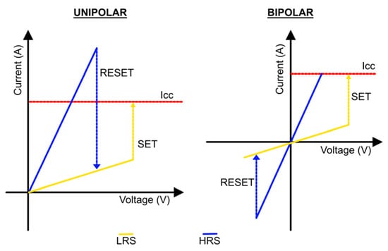
According to the current polarity, the RRAM can be divided into two modes: unipolar and bipolar (Figure 1). In unipolar switching, changing between modes does not depend on the polarity of the applied voltage. In bipolar switching, the SET and RESET processes rely on the polarity of the applied voltage. A switch from an HRS to an LRS occurs at one polarity (positive or negative) and the opposite polarity shifts the RRAM cell back into the HRS [3]. Resistance-switching properties in memristive devices were highly dependent on materials, device structures, external simulations, and switching mechanisms. Therefore, many reports deal with the adjustment of switching behavior characteristics by modifying the structure of the device and the simulation parameters [11][15][11,15].Figure 1.
Unipolar and bipolar modes for RRAM devices.
2.2. Activation Process
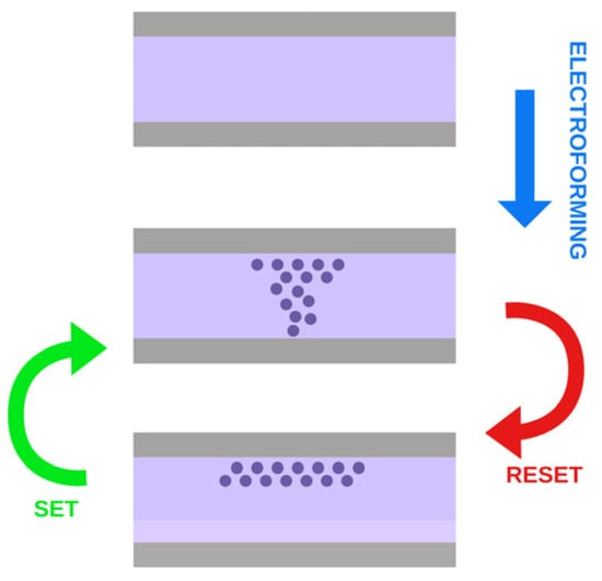
The RRAM behavior is based on the possibility of electrically modifying the conductivity of a stack of metal–insulator–metal (MIM). To activate the switching mechanism, some technologies require a preliminary formation operation [16][18], which is shown in Figure 2. The electroforming process (soft or hard) is usually realized by applying a large electrical bias across the two electrodes within a certain specific time interval to generate initial conductive channels via the Joule heating effect. The formation step can be conquered by appropriately modifying the fabrication process to readily introduce oxygen vacancies to facilitate the migration of anions within the switching layer [6]. Even if the forming process is performed once, this initial state plays a fundamental role in determining the subsequent array and system performance. The performance of the formation process relies on its ability to create homogeneous conductive conditions among cells, thus easing successive SET/RESET operations [16][18]. As explanations of the driving force of anion transport during the formation process, the following are suggested: (i) drift by electric potential gradient, (ii) electromigration assuming an electron kinetic energy, (iii) Fick diffusion due to ion concentration gradient, and (iv) thermophoresis due to temperature gradient [6].Figure 2.
Process of electroforming, SET and RESET.