Your browser does not fully support modern features. Please upgrade for a smoother experience.
Please note this is a comparison between Version 1 by Abdulaziz Alkhaldi and Version 2 by Jason Zhu.
The conventional boost DC/DC converter is used to step up the input voltage to a desired higher level within the practical limit required by the load with very few components. Stepping up the voltage is achieved by storing the energy in the inductor and releasing it to the output at a higher voltage. The boost converter is very popular for capacitive load applications such as photo-flashers and battery chargers. It is also used in automotive applications, power amplifiers, adaptive control applications, battery power systems, consumer electronics, DC motor drives and power factor correction circuits.
- high voltage gain
- DC/DC converter
- step-up techniques
1. High Step-Up Techniques
High step-up DC/DC converters, which are used for voltage boosting, are mainly classified as switched capacitors (SCs) (or charge pumps (CPs)), voltage multipliers (VM), switched inductor (SL), voltage lift (VL) and converters with multistage/multilevel structures. Depending on the application, these have merits and demerits in terms of cost, complexity, power density, reliability and efficiency. Some of the families classified are distinct to one known technique such as switched capacitor, voltage lift and switched inductor. Other families are extended to a few subfamilies such as the multi-stage family where it has been extended to cascaded, interleaved and multilevel.
2. Multistage/Multilevel Structures
One of the simplest methods of stepping up voltage is connecting various stages of a converter. This can be implemented by integrating symmetric or different converter modules (non-symmetric) with various high voltage gain techniques. The voltage gain increases linearly as a function of the topology used. Broadly, such topologies can be further classified as cascaded, interleaved and multilevel.
2.1. Cascaded Topology
2.1.1. Symmetric and Non-Symmetric Converters
In the general setup of cascaded DC/DC converters Figure 1a,b, two or more symmetric or non-symmetric converters that use two or more controllable switches [1][2][3][17,18,19] or a single switch [4][5][6][20,21,22] can be connected to increase the voltage gain without high duty cycle operation.
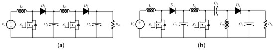
Figure 1. General Configuration of Cascaded DC/DC Converter (a) Symmetric (b) Non-symmetric.
As seen in Figure 2a, the low voltage stress on the power switch in the first stage of the cascade enables high frequency operation. A low frequency operates in the second stage [7][8][23,24]; hence, the switching losses are reduced [2][18]. However, a cascaded circuit has two sets of power devices, which makes it not only complex but also expensive [9][25]. Moreover, both power devices need to be synchronised to prevent the beat frequency from causing circuit stability issues [10][26]. An n-stage cascade boost converter with a single active switch is presented in [11][12][27,28]; such converters are an alternative solution for decreasing the total losses caused by active switches, as shown in Figure 2b. Moreover, they have a simple control circuitry. A comparative study on boost and zeta converters is presented in [13][29]. A single switch step-up DC/DC converter based on the new SEPIC technology and buck/boost converter [14][30] is shown in Figure 2c. Its voltage gain is higher than those of SEPIC and buck/boost converters. Therefore, the voltage stress on the power switch is low, and the input current is continuous. An integrated double boost and SEPIC converter (IDBS) is presented in [15][31] as shown in Figure 2d; it can attain a high voltage conversion ratio at a low duty cycle. The advantages of this combination converter are its capability to achieve a high step-up voltage gain (boost) and a low input current ripple (SEPIC).
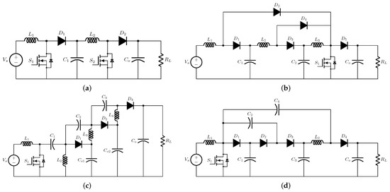
Figure 2. Cascaded Topologies for Symmetric and Non-symmetric Converters. (a) Double Boost Converter (DBC), (b) N-Stage Boost Converter, (c) SEPIC based on Buck-Boost Converter and (d) Double Boost SEPIC Converter.
2.1.2. Quadratic Boost Converters (QBC)
Figure 3 illustrates the general setup of a quadratic boost converter which comprises one switch, three diodes and four passive elements. A high step-up voltage gain can be obtained by using a quadratic converter Figure 3 at a moderate duty cycle [6][16][22,32], but the main drawback of such converters is that the voltage stress on the power switch is equal to the output voltage. Therefore, efficiency is compromised. The conventional quadratic boost converter has a limited voltage gain and is thus unsuitable for high-step-up applications.
Figure 3. General Setup of Quadratic Boost Converter (QBC).
Figure 4a shows a quadratic boost converter with a modified VL cell [17][33]; it achieves a high voltage gain at the output side. Furthermore, it reduces the voltage stress on the power switch, which is an issue with traditional quadratic boost converters. In the literature [18][19][20][21][22][23][24][25][26][27][28][29][30][31][32][33][34][35][36][34,35,36,37,38,39,40,41,42,43,44,45,46,47,48,49,50,51,52], many DC/DC converters based on quadratic boost converters and modified quadratic boost converters have been proposed to inhibit the dominant constraints in conventional boost converters. A quadratic following boost converter (QFBC) is presented in [22][38]. It consists of two switches, three capacitors, three diodes and two inductors, and it can step up the voltage gain at a moderate duty cycle. In the modified QFBC (MQFBC) proposed in [23][39], a bootstrap network is integrated to improve the conventional boost converter. In Figure 4b, a high voltage gain and reduced voltage stress are achieved by using a quadratic boost converter with a coupled inductor [24][25][40,41]. However, the power switch suffers from a high voltage stress caused by the leakage inductance of the coupled inductor. Passive clamping circuits are adopted to reduce this high voltage stress. The quadratic boost converter and SEPIC topologies in Figure 4c, which are presented in [26][42], increase the voltage conversion ratio without an extreme duty ratio. This converter takes advantage of two well-known DC/DC converters, namely, a quadratic boost converter, which has a high step-up capability, and a SEPIC converter which can reduce the input current ripple. A quadratic SEPIC with a switched-coupled inductor, shown in Figure 4d, is proposed in [27][43] to increase the voltage gain. In [28][44], a quadratic boost converter and a zeta converter are proposed for a high voltage gain and efficiency. Additionally, both the input and output current ripples are low (features of the quadratic boost converter and zeta converter, respectively). A quadratic boost converter and a Ćuk converter are combined in [29][45] to provide a high step-up voltage. Two configurations of this proposed converter are shown in Figure 4e,f. The configuration in Figure 4e is called hybrid QBC type I and its voltage stress is lower than the output voltage of the converter. The configuration in Figure 4f is called hybrid QBC type II, and its voltage gain is higher than that of hybrid QBC type I. A novel quadratic boost converter with low inductor currents is proposed in [30][46]; it can increase the voltage gain as well as the conventional quadratic boost converter can. Furthermore, it has a non-pulsating input current and low voltage stress on the power switch. The main drawback of this converter is its use of two switches. A hybrid cascaded DC/DC converter usually consists of a quadratic boost converter and voltage multiplier circuits. A high voltage gain in [31][47] is achieved by using a quadratic boost converter and a coupled inductor with an extended voltage doubler cell. Quadratic boost with a voltage multiplier cell was proposed in [32][48], the output voltage is much higher under the same duty cycle of the traditional quadratic boost converter. Moreover, the input current ripple is low, and the voltage stress is reduced.
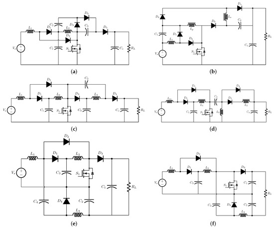
Figure 4. Cascaded Topology of Conventional Quadratic Boost Converter. (a) QBC based on VL, (b) QBC based on Coupled Inductor, (c) QBC and SEPIC Converters, (d) QBC-SEPIC based on SC and coupled Inductor, (e) QBC and Ćuk Converter Type-I and (f) QBC and Ćuk Converter Type-II.
2.2. Interleaved Converters
The interleaved step-up DC/DC converter consists of passive or active clamp circuits and voltage multiplier modules between the input switches and the output diode for providing a high voltage conversion ratio. However, this technique decreases the current ripple and increases the power density because the input current level in the step-up DC/DC converters is higher than the output current level. Various interleaved DC/DC converters with different techniques can be found in the literature [37][38][39][40][41][42][43][44][45][46][53,54,55,56,57,58,59,60,61,62].
In Figure 5a, the interleaved converter with voltage multiplier cell proposed in [37][53] can reduce the input current ripple and improve the power level because the interleaved structure is employed at the input side. Furthermore, the voltage gain is increased at the output side because of the voltage multiplier cell. In Figure 5b, a conventional interleaved boost converter achieves high voltage gain by integrating a voltage multiplier module consisting of switched capacitors and coupled inductors [38][39][54,55]. Additionally, it can reduce the input current ripple and doubles the power transfer. In order to increase the voltage gain, the interleaved quadratic boost DC/DC converter has been proposed by using two structures of quadratic boost converter as shown in Figure 5c. It can achieve the voltage gain by using a voltage lift capacitor [40][56]. In [41][57], an interleaved step-up converter with a single capacitor snubber is presented. A Winding Crossed Coupled Inductor (WCCI) has been presented in [42][58] consisting of three winding coupled inductors to boost the voltage gain. In addition, the first phase has two windings, while the second phase has the third winding. To recycle the leakage energy and absorb the voltage spike caused by the leakage inductance, either a passive clamp or an active clamp is adopted [43][59]. In [44][60], the proposed converter is an interleaved high step-up DC/DC converter combining with three techniques. However, it takes the advantage of the coupled inductor, switched capacitor and the conventional interleaved boost converter. In order to increase the voltage conversion ratio without using a coupled inductor, a non-isolated high gain interleaved DC/DC converter with reduced voltage stress on semiconductor devices has been proposed in [45][61]. In Figure 5d, the proposed converter contains two interleaved modified step-up KY converters. The voltage gain is higher than the conventional interleaved boost, Ćuk, ZETA and SEPIC converters. The voltage stress on the semiconductor devices is low; therefore, the efficiency of the proposed converter is increased due to low on-state resistance and low conduction loss. A high step-up interleaved DC/DC converter by combining voltage multiplier and coupled inductor has been proposed in [46][62]. Two coupled inductors and voltage multiplier are utilised to provide a very high step-up voltage gain; hence, the input current ripple is low because the proposed converter uses the interleaved boost converter at the input side. In addition, it can alleviate the reverse recovery current problem of the diode, and it recycles the leakage energy. Eventually, the efficiency of the proposed converter can be improved by implementing low-voltage-rated MOSFETs with a small on-state resistance which can reduce the conduction loss.
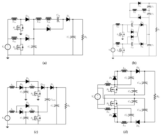
Figure 5. Interleaved Converters. (a) Interleaved with VMC and Coupled Inductor, (b) Interleaved with VMC based on SC and Coupled Inductor, (c) Interleaved QBC and (d) Tow Interleaved Modified Step-Up KY Converters.
2.3. Multilevel Converters
A Multilevel DC/DC converter helps to decrease or nearly eliminate the magnetic components leading to desirable cost, size, weight, and managing high-temperature operation [47][63]. Concerning the input voltage, multiple level converters can be categorised into single DC and multiple DC sources groups. Single source multilevel structures are majorly used in electric or fuel cell-based vehicles and traction motors. In contrast, the multiple DC source multilevel converters with cascaded structures are used in modular renewable energy sources such as PV or fuel cells [48][16].
The switch capacitor structures are usually used in multilevel converter. The Capacitor-Clamped module for multilevel converters in Figure 6a is an essential module for boosting the voltage level, which contains three switches and one capacitor [49][50][51][64,65,66]. In [52][67], double the DC input voltage can be achieved by utilising two capacitors and four switches, as shown in Figure 6b. PV modules can increase the output voltage level by using a series connection; hence, the DC/DC converter should be used with each PV module to maintain the voltage regulated. The advantages of this connection are higher reliability, higher safety/protection, low maintenance and lower cost [53][68]. This converter is well known as the Modular Multilevel Converter (MMC) [54][55][56][69,70,71].
Figure 6. (a) Multilevel Modular Capacitor Clamped Converter (MMCCC) and (b) 6X Switched Capacitor.
Despite its features such as modularity structure, high power density, reliability, the MMC can provide high efficiency and high voltage/current levels. The fundamental multistage/level has shortcomings, such as a complex control scheme and many components. All of this will be relatively heavy, large and bulky. This technique can be used in HVDC transmission, renewable energy systems, DC microgrids, high power DC supply and space technology.
3. Switched Capacitor (SC)
Topologies using SCs are majorly used in low power electronic applications, especially in systems with limited physical dimensions involving higher power density [57][72]. The concept of SCs is based on charge pump (CP), which is the number of capacitors used in SC cell where the high step-up ratio is attainable [58][59][60][61][73,74,75,76]. It comprises only capacitors, MOSFETs and diodes, and does not include any inductive element. Their characteristics allow monolithic integration, minimised levels of EMI, and reduced weight and volume [62][77]. Depending on the non-inverting and inverting cell terms, the polarity of input and output voltages are the same or opposite [63][78]. As shown in Figure 7, it consists of two capacitors and three diodes, and is placed in conventional DC/DC converters (such as Zeta, SEPIC and Ćuk converters) to build a new converter. The voltage divider circuit describes the functionality of the new converters. During the ON state of the diodes (D1and D2), the capacitors (C1 and C2) are charged in parallel. During the OFF state of the diodes (D1 and D2), the capacitors (C1 and C2) are charged in series. From Figure 7a,e, non-inverting SC or inverting SC are used in many different step-up DC/DC converters. Figure 7a,b are non-inverting and inverting SC cell Zeta converters, respectively. It is developed by utilising the cell of non-inverting and inverting SC instead of the capacitor, the output inductor and the output diode of the conventional Zeta converter. As a result of the additional components, the voltage gain is higher than that achieved by a conventional Zeta converter. Moreover, there is a lower voltage stress on the power switch. Figure 7c depicts a SEPIC converter based on a non-inverting SC cell. Instead of the conventional SEPIC converter’s output diode, the non-inverting SC cell is employed. Compared to a conventional SEPIC converter, it improves the voltage conversion ratio and decreases the voltage stress on the main switch. Figure 7d represents an inverting SC cell Ćuk converter. It is established by modifying the conventional Ćuk converter’s capacitor, output inductor and output diode with an inverted SC cell. However, it boosts the voltage conversion ratio and decreases the switch’s voltage stress. While Figure 7e is a similar circuit to Figure 7d, the voltage doubler cell has been added to the output side. Thus, the voltage gain is higher than the prior circuit and has lower voltage stress. In addition, the Ćuk converter has inductors on both sides, so current flows continuously in both directions. Combining both coupled inductor and switched capacitor [64][79], an ultra-high step-up DC/DC converter with low voltage stress and high efficiency has been achieved. It does not need extra windings for an ultra-high step-up conversion ratio. In addition, the passive clamp circuit can recycle the leakage energy, which can avoid the voltage spikes across the switch, and the efficiency is increased. The voltage stress on the main switch is lower than the other converter, and it maintains steady for the entire duty cycle range. Moreover, the reverse recovery current problem of the diode is alleviated through the leakage inductance of the coupled inductor.
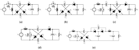
Figure 7. Switched Capacitor (SC) Techniques. (a) Zeta Converter based on Non-inverting SC Cell, (b) Zeta Converter based on Inverting SC Cell, (c) SEPIC Converter based on Non-inverting SC Cell, (d) Ćuk Converter based on Inverting SC Cell and (e) Ćuk Converter with Voltage Doubler based on Inverting SC Cell.
There are five standard techniques based on SC: Voltage Doubler, Ladder, Dickson, Makowski or Fibonacci, and Series-Parallel. The Voltage Doubler SC is based on two phases, where the switching devices are turning ON and OFF in complement, and the output voltage is double the value of the input voltage [65][80]. The ladder SC consists of two sets of capacitors. Therefore, the capacitor of the lower ladder is changing the input voltage node, which is made different voltage gain [65][80]. The Dickson SC can be utilised as a voltage multiplier. In the Dickson SC, the diodes are used to charge pumps instead of active switches. Two strings of pulses with proper phase shift are needed to drive the switching devices, typically at tens of kilohertz or up to megahertz. Another technique based on SC is the Makowski SC; it is also known as Fibonacci because its voltage gain can be boosted according to the Fibonacci number. However, the Makowski SC requires fewer devices to obtain high voltage gain [48][16]. The voltage regulation ranges of techniques have been limited, and the voltage gains of the circuit are predetermined.
An inductor can be utilised in this topology by replacing one active switch in the five standards SC to achieve higher step-up gain and broad voltage regulations [66][81]. In order to increase the voltage conversion ratio of step-up DC/DC converter, non-isolated high step-up soft-switching DC/DC converter by using interleaving and Dickson SC techniques have been presented [67][82]. The advantage of this proposed converter is an improved voltage conversion ratio due to the Dickson SC technique. They can alleviate high current spikes by adding a small resonant inductor into the Dickson SC technique [68][69][83,84]. In addition, it can reduce the input current ripple and increase the power density due to interleaving operation.
4. Voltage Multiplier
Voltage Multiplier circuits contain diodes and capacitors to provide high DC voltage at the output side. Hence, it is efficient, low cost and has a simple structure. The Voltage Multipliers are majorly classified into Voltage Multiplier cells (VMC) and Voltage Multiplier Rectifier (VMR). VMC can be placed after the main switch to reduce its voltage stress. Moreover, a high voltage conversion ratio and higher efficiency are the other advantages of the VMC. VMR can be placed at the output stage of the transformer or coupled inductor. However, it helps to rectify the AC or pulsating DC voltage. Meanwhile, it acts as a voltage multiplier [48][16].
In many applications, the multiplication of the input voltage is applied; hence, various structures have been famous in these cells. In addition, it has low weight, size and cost even if the operation is at high frequency because the bulky capacitors are not used [70][85]. Some VMCs are also known as switched-diode capacitor voltage multiplier cells, which only contain diodes and capacitors [71][86]. For a higher voltage conversion ratio, the inductors of some VMC is required [63][78]; hence, the power switch can operate with zero current switching (ZCS) [70][85]. The modified conventional boost converter and modified voltage multiplier cell present a high gain non-isolated DC/DC converter [72][87]. In [73][88], a high step-up DC/DC converter based on SEPIC converter is introduced by adopting a coupled inductor with voltage multiplier cell. Low input current ripple, high voltage gain and higher efficiency are the advantages of this converter, which combines two voltage boosting techniques with a SEPIC converter. High step-up DC/DC converter based on a new modified single switch SEPIC (-SEPIC) is proposed in [74][89]. The output voltage gain can be achieved by adding a coupled inductor and voltage multiplier rectifier (VMR). The advantages of the -SEPIC are continuous input current, zero current switching (ZCS) and low reverse recovery loss. Therefore, the voltage spike on the main switch is low.
There are many different configurations of Half-wave [75][90] or Full-wave voltage multipliers that contain diodes and capacitors [76][91]. The Greinacher Voltage Doubler Rectifier (G-VD) is illustrated in Figure 11c, which is used in many DC/DC converters at the output stage of transformer-based converter or multistage converters with modular series output [77][92]. The shortage of the VMR is the high voltage stress on diodes, and output capacitor voltage is equal to the output voltage. The Cockcroft–Walton (CW) is another voltage multiplier, same as G-VMR, introduced in different year, but it is famous for its cascading structure [78][93]. A full-bride voltage doubler rectifier is commonly used in various DC/DC converters because its voltage stress on the output capacitor is half the output voltage [79][80][94,95]. Sometimes the VMR is considered a voltage triple rectifier; therefore, it can be used in many ultra-step-up DC/DC converters. In isolated structures and multilevel output series structures, the VMR can be applied [81][96]. Despite its features, such as high voltage ability with simple topology and cell-based structure, voltage multiplier can be integrated into various converters. The voltage multiplier also has shortcomings, such as high voltage stress on components. This needs several cells for high voltage application. This technique can be used in medical (X-ray, laser), high power laser and physics (plasma research, particle accelerator) applications.
5. Voltage Lift (VL)
The presence of parasitic elements restricts the output voltage and causes poor transfer efficiency of DC/DC converters. The voltage lift technique provides an excellent opportunity to improve circuit characteristics. The basic structure of the voltage lift is shown in Figure 8. A popular converter that uses VL technique is Luo converter which has been introduced in [82][83][97,98]. The capacitor is charged to a specific voltage, and the output voltage is lifted with the voltage level of a charged capacitor.
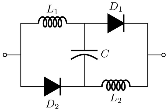
Figure 8. Basic Structure of Voltage Lift (VL) Cell.
Depending on the number of capacitors in the circuit, the output voltage can be further re-lifted, triple-lifted and quadruple lifted by reapplying the method as shown in Figure 9a [84][85][86][99,100,101]. The significant advantages of this topology are high power density, high efficiency and cost-effectiveness. In addition, the output voltage ripple is small for high voltage applications. In the literature, various converters, namely, the Ćuk, SEPIC and Zeta converters apply the VL technique [87][88][102,103]. The N-Stage quadratic boost converter based on the voltage life technique and voltage multiplier (NQBC-VLVM) described in [21][37]. By replacing the input inductor of NQBC-VLVM with the VL technique, the voltage conversion ratio with a small duty cycle can be improved. Additionally, the voltage gain can be multiplied by two, which is a benefit of VM, and the voltage stress on the main switch is half the output voltage, leading to higher efficiency. A quadratic boost converter with voltage doubler and voltage life technique is presented in [89][90][104,105], which increases the voltage gain four times by utilising the VL technique as shown in Figure 9b. In addition, it can double the voltage gain by using a voltage doubler cell and reduce the voltage stress to half of the output voltage on the main switch. The quadratic boost converter based on the elementary VL technique is proposed in [91][106] to obtain high voltage gain. Depending on the number of inductors, the proposed converter can exponentially step up the voltage gain. Therefore, the voltage gain of the double lift circuit in Figure 9c is eight times the input voltage, and the voltage gain of the triple lift in Figure 9d is nearly 16 times the input voltage. In contrast, the efficiency decreases with the increase of the number of inductors. In [92][107], cascaded boost converter based on the double VL technique is proposed. The first stage output of this converter becomes the second stage’s input voltage; hence, it can achieve high voltage gain and low voltage stress on the switches at a low duty cycle.
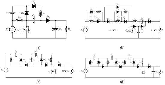
Figure 9. Voltage Lift (VL) Techniques. (a) Boost Converter based on VL, (b) QBC based on Voltage Doubler and VL, (c) QBC based on elementary VL (Double Lift) and (d) QBC based on elementary VL (Triple Lift).
6. Switched Inductor (SL)
The basic Switched Inductor (SL) cell is illustrated in Figure 10. The main operation of such cell is that inductors are charged in parallel and discharged in series. This kind of operation was first introduced in [71][86]. The input inductor replaces a hybrid boost converter in a conventional boost converter to switched inductor circuit. Hence, it provides a higher voltage gain than the conventional boost converter.
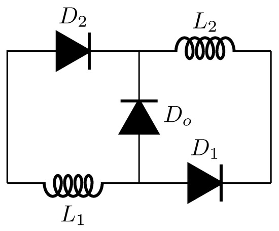
Figure 10. Basic Switched Inductor (SL) Cell.
These two inductors can be integrated into a single inductor because they have the same inductance, which helps reduce the size and weight of the converter. Recently, a high voltage conversion ratio DC/DC converter has been achieved by adding a small resonant inductor to the primary VL cell’s circuit and replacing the output diode (Do) [93][108]. A simple structure and high efficiency are the main advantages of this converter. The self-lift SL cell is formed by implementing the elementary VL cell in the SL cell, and the double self-lift SL cell is formed by adding another diode and capacitor to the self-lift SL cell [94][109]. Therefore, the double self-lift SL cell switch is an operation in reverse using (So) instead of (Do) the primary SL cell. For high voltage gain, a transformer-less step-up DC/DC converter based on a switched inductor (SL) and switched capacitor (SC) techniques have been proposed in [95][110]. Furthermore, it can reduce the voltage stress on the semiconductor switches, but the cost will increase because of the two switches.
7. Magnetic Coupling
One of the most popular voltage boosting techniques is magnetic coupling, which is used in many DC/DC converters as either non-isolated or isolated converters. The outstanding feature of magnetic coupling is its ability to achieve a higher voltage gain in the output by turning the windings beside the switch duty cycle [96][114]. The magnetic coupling though has some problems such as leakage inductance [97][115]. Broadly, it can be further classified as transformer, coupled inductor or multi-track topologies.7.1. Transformer
An electrical isolated DC/DC converter requires a medium/high frequency transformer. There are several isolated DC/DC converters that use such device such as full or half-bridge converter, forward converter, push-pull converter and flyback converter. In the past decade, the performance of the conventional DC/DC converter for many applications has been enhanced by using isolated DC/DC converters [98][99][100][101][102][103][104][116,117,118,119,120,121,122].7.2. Coupled Inductor
Since isolation is not required in many applications, coupled inductor circuits can take the advantage of transformer coupling without isolation to increase the voltage in DC/DC converters [105][106][107][108][109][110][111][112][113][114][123,124,125,126,127,128,129,130,131,132]. Figure 11 shows a general setup for a step-up converter with coupled inductor. The voltage source is a secondary winding, while the clamp capacitor and diode are used to recover the leakage energy recycled directly or through the secondary winding to the load [105][123]. In addition, a snubber circuit can be used to absorb the energy of the leakage inductance and to improve efficiency [106][124] as shown in Figure 12a. In [107][125], a higher voltage gain can be achieved by using a combination of the charge pump and switched capacitor voltage multiplier with a coupled inductor, as shown in Figure 12b, which is helpful in distributed generation systems. A non-isolated high step-up DC/DC converter with continuous input current integrating coupled inductor is introduced in [115][133] and shown in Figure 12c. It consists of three diodes, three capacitors and one inductor. Further, the coupled inductor in this converter is employed, which achieves higher voltage gain and low input current ripple because the inductor is connected in series to the input. The clamp circuit reduces the voltage stress on the main switch. As a result, low on-state resistance RDS(ON) can be achieved, which helps to reduce the conduction losses. Therefore, the switching loss is reduced when the switch is turned on under zero current. A single switch high voltage gain and high-efficiency DC/DC converter are proposed in [116][134]. The voltage gain is achieved by charging the intermediate capacitors through the coupled inductor in parallel and discharging in series. In [117][135], a high step-up DC/DC converter based on three winding coupled inductors using two Cockcroft–Walton was proposed, as shown in Figure 12d. Impedance (Z-) source is another area of research in high step-up DC/DC converters. It can increase the voltage gain by using a small duty cycle [118][119][120][121][122][136,137,138,139,140].
Figure 11. General Setup of the Coupled Inductor Circuit.
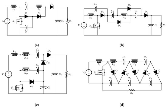
Figure 12. Coupled Inductor Techniques. (a) Boost Converter based on Coupled Inductor, (b) Boost Converter based on Two Capacitors and Coupled Inductor, (c) Boost Converter based on a Coupled Inductor and (d) Boost Converter with 3-winding Coupled Inductor.