With the rapid development of artificial intelligence and the Internet of Things, there is an explosion of available data for processing and analysis in any domain. However, signal processing efficiency is limited by the Von Neumann structure for the conventional computing system. Therefore, the design and construction of artificial synapse, which is the basic unit for the hardware-based neural network, by mimicking the structure and working mechanisms of biological synapses, have attracted a great amount of attention to overcome this limitation. In addition, a revolution in healthcare monitoring, neuro-prosthetics, and human–machine interfaces can be further realized with a flexible device integrating sensing, memory, and processing functions by emulating the bionic sensory and perceptual functions of neural systems. Therefore, low-dimensional materials, including both 0-dimensional materials (0D), one-dimensional (1D) materials, and two-dimensional (2D), have been employed in flexible neuromorphic devices and systems.
- artificial synapse
- memristor
- transistor
1. Introduction
2. Low-Dimensional Materials
With the development of material science and processing technology, several novel materials with distinct electrical and physical properties have been discovered and synthesized. Among them, low-dimensional materials with at least one dimension at the nanoscale level, have distinct properties from their corresponding bulk materials [35]. Due to their outstanding properties, low-dimensional materials have attracted a great amount of attention [36,37,38,39,40][36][37][38][39][40]. For example, 2D materials, such as transitional metal dichalcogenides (TMDs), 2D oxides, and MXene, and 1D materials, such as carbon nanotubes, metal oxide nanotubes, and silicon nanowires, have been synthesized and widely applied. In addition, 0D materials, such as quantum dots and nanoparticles, were used in the dielectric layer of a memristive device [26,27,41][26][27][41]. These materials show superior flexibility for the implementation of flexible electronics than their bulk counterparts. Mechanical flexibility allows the devices to stably adhere on the surfaces of an arbitrary object, including human skin and organs, as shown in Figure 1. [42]. In addition, the electrical properties of low-dimensional materials range from insulators to conductors, and a number of flexible electronics, ranging from flexible electrodes to heterostrcure devices consisting of both insulators and conductors, can be fabricated with low-dimensional materials. Furthermore, the properties can be tuned by various methods, which will further contribute to the various applications of low-dimensional materials. For example, the electrical and physical properties of 2D materials can be tuned by adjusting the layer or doping with other elements [43]. For1D and 0D materials, the modification of the surface morphology and the functional groups can also change the properties [44,45][44][45]. In addition, size, diameter, and surface roughness will also lead to a variety of electrical and physical properties of low-dimensional materials [46,47][46][47].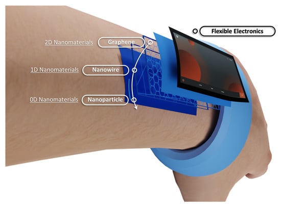
| 0D Material | 1D Material | 2D Material | |
|---|---|---|---|
| Synthesis of the materials | Easy | Medium | Difficult |
| Material stability | Medium | High | Low |
| Type of synaptic device | Memristor | Memristor/Transistor | Memristor/Transistor |
| Device fabrication | Easy | Difficult | Medium |
| Wafer scale fabrication | Easy | Difficult | Difficult |
| Uniformity | Low | Low | High * |
2.1. Zero Dimensional Materials
2.2. One-Dimensional Materials
2.3. Two-Dimensional Materials
References
- Von Neumann, J. First Draft of a Report on the EDVAC. IEEE Ann. Hist. Comput. 1993, 15, 27–75.
- McKee, S. Reflections on the Memory Wall. In Proceedings of the 1st Conference on Computing Frontiers, Ischia, Italy, 14–16 April 2004.
- Merolla, P.A.; Arthur, J.V.; Alvarez-Icaza, R.; Cassidy, A.S.; Sawada, J.; Akopyan, F.; Jackson, B.L.; Imam, N.; Guo, C.; Nakamura, Y.; et al. A million spiking-neuron integrated circuit with a scalable communication network and interface. Science 2014, 345, 668.
- Markram, H. The blue brain project. Nat. Rev. Neurosci. 2006, 7, 153–160.
- Nawrocki, R.A.; Voyles, R.M.; Shaheen, S.E. A mini review of neuromorphic architectures and implementations. IEEE Trans. Electron Devices 2016, 63, 3819–3829.
- Wang, X.J.; Zhou, Z.; Ban, C.Y.; Zhang, Z.P.; Ju, S.; Huang, X.; Mao, H.W.; Chang, Q.; Yin, Y.H.; Song, M.Y.; et al. Multifunctional polymer memory via bi-interfacial topography for pressure perception recognition. Adv. Sci. 2020, 7, 1902864.
- Groothuis, S.S.; Folkertsma, G.A.; Stramigioli, S. A general approach to achieving stability and safe behavior in distributed robotic architectures. Front. Robot. AI 2018, 5, 108.
- Field, D.J. What is the goal of sensory coding? Neural Comput. 1994, 6, 559–601.
- Cohen, J.; Peristein, W.; Braver, T.; Nystrom, L.; Noll, D.C.; Jonides, J.; Smith, E.E. Temporal dynamic of brain activation during a working-memory task. Nature 1997, 386, 604–607.
- Berridge, M.J. Neuronal calcium signaling. Neuron 1998, 21, 13–26.
- Sun, F.; Lu, Q.; Feng, S.; Zhang, T. Flexible artificial sensory systems based on neuromorphic devices. ACS Nano 2021, 15, 3875–3899.
- Sebastian, A.; Le Gallo, M.; Khaddam-Aljameh, R.; Eleftheriou, E. Memory devices and applications for in-memory computing. Nat. Nanotechnol. 2020, 15, 529–544.
- Zhou, F.; Chai, Y. Near-sensor and in-sensor computing. Nat. Electron. 2020, 3, 664–671.
- Jang, B.C.; Kim, S.; Yang, S.Y.; Park, J.; Cha, J.H.; Oh, J.; Choi, J.; Im, S.G.; Dravid, V.P.; Choi, S.Y. Polymer analog memristive synapse with atomic-scale conductive filament for flexible neuromorphic computing system. Nano Lett. 2019, 19, 839–849.
- Sangwan, V.K.; Hersam, M.C. Neuromorphic nanoelectronic materials. Nat. Nanotechnol. 2020, 15, 517–528.
- Park, H.L.; Lee, Y.; Kim, N.; Seo, D.G.; Go, G.T.; Lee, T.W. Flexible neuromorphic electronics for computing, soft robotics, and neuroprosthetics. Adv. Mater. 2020, 32, 1903558.
- Fu, T.; Liu, X.; Fu, S.; Woodard, T.; Gao, H.; Lovley, D.R.; Yao, J. Self-sustained green neuromorphic interfaces. Nat. Commun. 2021, 12, 3351.
- Ge, J.; Li, D.; Huang, C.; Zhao, X.; Qin, J.; Liu, H.; Ye, W.; Xu, W.; Liu, Z.; Pan, S. Memristive synapses with high reproducibility for flexible neuromorphic networks based on biological nanocomposites. Nanoscale 2020, 12, 720–730.
- Guo, T.; Ge, J.; Sun, B.; Pan, K.; Pan, Z.; Wei, L.; Yan, Y.; Zhou, Y.N.; Wu, Y.A. Soft Biomaterials Based Flexible Artificial Synapse for Neuromorphic Computing. Adv. Electron. Mater. 2022, 8, 2200449.
- Nguyen-Dang, T.; Harrison, K.; Lill, A.; Dixon, A.; Lewis, E.; Vollbrecht, J.; Hachisu, T.; Biswas, S.; Visell, Y.; Nguyen, T.Q. Biomaterial-Based Solid-Electrolyte Organic Electrochemical Transistors for Electronic and Neuromorphic Applications. Adv. Electron. Mater. 2021, 7, 2100519.
- Vendamme, R.; Onoue, S.Y.; Nakao, A.; Kunitake, T. Robust free-standing nanomembranes of organic/inorganic interpenetrating networks. Nat. Mater. 2006, 5, 494–501.
- Kim, D.H.; Xiao, J.; Song, J.; Huang, Y.; Rogers, J.A. Stretchable, curvilinear electronics based on inorganic materials. Adv. Mater. 2010, 22, 2108–2124.
- Lu, Q.; Sun, F.; Liu, L.; Li, L.; Wang, Y.; Hao, M.; Wang, Z.; Wang, S.; Zhang, T. Biological receptor-inspired flexible artificial synapse based on ionic dynamics. Microsyst. Nanoeng. 2020, 6, 84.
- Liang, S.-J.; Li, Y.; Cheng, B.; Miao, F. Emerging Low-Dimensional Heterostructure Devices for Neuromorphic Computing. Small Struct. 2022, 3, 2200064.
- Jin, T.; Gao, J.; Wang, Y.; Chen, W. Flexible neuromorphic electronics based on low-dimensional materials. Sci. China Mater. 2022, 65, 2154–2159.
- Khan, M.; Mutee Ur Rehman, H.M.; Tehreem, R.; Saqib, M.; Rehman, M.M.; Kim, W.-Y. All-Printed Flexible Memristor with Metal–Non-Metal-Doped TiO2 Nanoparticle Thin Films. Nanomaterials 2022, 12, 2289.
- Younis, A.; Chu, D.; Lin, X.; Yi, J.; Dang, F.; Li, S. High-performance nanocomposite based memristor with controlled quantum dots as charge traps. ACS Appl. Mater. Interfaces 2013, 5, 2249–2254.
- Ren, Z.; Nie, J.; Shao, J.; Lai, Q.; Wang, L.; Chen, J.; Chen, X.; Wang, Z.L. Fully elastic and metal-free tactile sensors for detecting both normal and tangential forces based on triboelectric nanogenerators. Adv. Funct. Mater. 2018, 28, 1802989.
- Ren, Z.; Ding, Y.; Nie, J.; Wang, F.; Xu, L.; Lin, S.; Chen, X.; Wang, Z.L. Environmental energy harvesting adapting to different weather conditions and self-powered vapor sensor based on humidity-responsive triboelectric nanogenerators. ACS Appl. Mater. Interfaces 2019, 11, 6143–6153.
- Ren, Z.; Nie, J.; Xu, L.; Jiang, T.; Chen, B.; Chen, X.; Wang, Z.L. Directly visualizing tactile perception and ultrasensitive tactile sensors by utilizing body-enhanced induction of ambient electromagnetic waves. Adv. Funct. Mater. 2018, 28, 1805277.
- Wang, F.; Ren, Z.; Nie, J.; Tian, J.; Ding, Y.; Chen, X. Self-powered sensor based on bionic antennae arrays and triboelectric nanogenerator for identifying noncontact motions. Adv. Mater. Technol. 2020, 5, 1900789.
- Wu, P.; He, T.; Zhu, H.; Wang, Y.; Li, Q.; Wang, Z.; Fu, X.; Wang, F.; Wang, P.; Shan, C. Next-generation machine vision systems incorporating two-dimensional materials: Progress and perspectives. InfoMat 2022, 4, e12275.
- Islam, M.M.; Krishnaprasad, A.; Dev, D.; Martinez-Martinez, R.; Okonkwo, V.; Wu, B.; Han, S.S.; Bae, T.-S.; Chung, H.-S.; Touma, J. Multiwavelength optoelectronic synapse with 2D materials for mixed-color pattern recognition. ACS Nano 2022, 16, 10188–10198.
- Yang, Q.; Luo, Z.D.; Zhang, D.; Zhang, M.; Gan, X.; Seidel, J.; Liu, Y.; Hao, Y.; Han, G. Controlled optoelectronic response in van der Waals heterostructures for in-sensor computing. Adv. Funct. Mater. 2022, 32, 202207290.
- Dresselhaus, M.S.; Chen, G.; Tang, M.Y.; Yang, R.; Lee, H.; Wang, D.; Ren, Z.; Fleurial, J.P.; Gogna, P. New directions for low-dimensional thermoelectric materials. Adv. Mater. 2007, 19, 1043–1053.
- Wang, J.; Jin, X.; Li, C.; Wang, W.; Wu, H.; Guo, S. Graphene and graphene derivatives toughening polymers: Toward high toughness and strength. Chem. Eng. J. 2019, 370, 831–854.
- Novoselov, K.S.; Geim, A.K.; Morozov, S.V.; Jiang, D.E.; Zhang, Y.; Dubonos, S.V.; Grigorieva, I.V.; Firsov, A.A. Electric field effect in atomically thin carbon films. Science 2004, 306, 666–669.
- Yin, W.; Tan, H.; Ding, P.; Wen, B.; Li, X.B.; Teobaldi, G.; Liu, L.-M. Recent advances in low-dimensional janus materials: A theory and simulation perspective. Mater. Adv. 2021, 1, 7543–7558.
- Zhang, A.; Wang, Z.; Ouyang, H.; Lyu, W.; Sun, J.; Cheng, Y.; Fu, B. Recent progress of two-dimensional materials for ultrafast photonics. Nanomaterials 2021, 11, 1778.
- Raagulan, K.; Kim, B.M.; Chai, K.Y. Recent advancement of electromagnetic interference (EMI) shielding of two dimensional (2D) MXene and graphene aerogel composites. Nanomaterials 2020, 10, 702.
- Sokolov, A.S.; Ali, M.; Riaz, R.; Abbas, Y.; Ko, M.J.; Choi, C. Silver-adapted diffusive memristor based on organic nitrogen-doped graphene oxide quantum dots (N-GOQDs) for artificial biosynapse applications. Adv. Funct. Mater. 2019, 29, 1807504.
- Park, J.; Hwang, J.C.; Kim, G.G.; Park, J.U. Flexible electronics based on one-dimensional and two-dimensional hybrid nanomaterials. InfoMat 2020, 2, 33–56.
- Wan, J.; Lacey, S.D.; Dai, J.; Bao, W.; Fuhrer, M.S.; Hu, L. Tuning two-dimensional nanomaterials by intercalation: Materials, properties and applications. Chem. Soc. Rev. 2016, 45, 6742–6765.
- Yang, S.; Liu, F.; Wu, C.; Yang, S. Tuning surface properties of low dimensional materials via strain engineering. Small 2016, 12, 4028–4047.
- Choudhary, K.; Cheon, G.; Reed, E.; Tavazza, F. Elastic properties of bulk and low-dimensional materials using van der Waals density functional. Phys. Rev. B 2018, 98, 014107.
- Kamlapure, A.; Simonato, M.; Sierda, E.; Steinbrecher, M.; Kamber, U.; Knol, E.J.; Krogstrup, P.; Katsnelson, M.I.; Rösner, M.; Khajetoorians, A.A. Tuning lower dimensional superconductivity with hybridization at a superconducting-semiconducting interface. Nat. Commun. 2022, 13, 4452.
- Liu, Y.; Xiao, C.; Li, Z.; Xie, Y. Vacancy engineering for tuning electron and phonon structures of two-dimensional materials. Adv. Energy Mater. 2016, 6, 1600436.
- Han, X.; Li, S.; Peng, Z.; Al-Yuobi, A.O.; Bashammakh, A.S.O.; Leblanc, R.M. Interactions between carbon nanomaterials and biomolecules. J. Oleo Sci. 2016, 65, 1–7.
- Fang, J.; Zhou, Z.; Xiao, M.; Lou, Z.; Wei, Z.; Shen, G. Recent advances in low-dimensional semiconductor nanomaterials and their applications in high-performance photodetectors. InfoMat 2020, 2, 291–317.
- Zhou, Z.; Zhang, H.; Liu, J.; Huang, W. Flexible electronics from intrinsically soft materials. Giant 2021, 6, 100051.
- Meng, J.L.; Wang, T.Y.; Chen, L.; Sun, Q.Q.; Zhu, H.; Ji, L.; Ding, S.J.; Bao, W.Z.; Zhou, P.; Zhang, D.W. Energy-efficient flexible photoelectric device with 2D/0D hybrid structure for bio-inspired artificial heterosynapse application. Nano Energy 2021, 83, 105815.
- Yu, H.; Wei, H.; Gong, J.; Han, H.; Ma, M.; Wang, Y.; Xu, W. Evolution of bio-inspired artificial synapses: Materials, structures, and mechanisms. Small 2021, 17, 2000041.
- Chen, T.; Yang, S.; Wang, J.; Chen, W.; Liu, L.; Wang, Y.; Cheng, S.; Zhao, X. Flexible Artificial Memristive Synapse Constructed from Solution-Processed MgO-Graphene Oxide Quantum Dot Hybrid Films. Adv. Electron. Mater. 2021, 7, 2000882.
- Liang, K.; Wang, R.; Huo, B.; Ren, H.; Li, D.; Wang, Y.; Tang, Y.; Chen, Y.; Song, C.; Li, F. Fully Printed Optoelectronic Synaptic Transistors Based on Quantum Dot-Metal Oxide Semiconductor Heterojunctions. ACS Nano 2022, 16, 8651–8661.
- Wang, K.; Dai, S.; Zhao, Y.; Wang, Y.; Liu, C.; Huang, J. Light-stimulated synaptic transistors fabricated by a facile solution process based on inorganic perovskite quantum dots and organic semiconductors. Small 2019, 15, 1900010.
- Vishwanath, S.K.; Kim, J. Resistive switching characteristics of all-solution-based Ag/TiO2/Mo-doped In2O3 devices for non-volatile memory applications. J. Mater. Chem. C 2016, 4, 10967–10972.
- Zou, C.; Sun, J.; Gou, G.; Kong, L.-A.; Qian, C.; Dai, G.; Yang, J.; Guo, G.-h. Polymer-electrolyte-gated nanowire synaptic transistors for neuromorphic applications. Appl. Phys. A 2017, 123, 57.
- Ting, Y.H.; Chen, J.Y.; Huang, C.W.; Huang, T.K.; Hsieh, C.Y.; Wu, W.W. Observation of resistive switching behavior in crossbar core-shell Ni/NiO nanowires memristor. Small 2018, 14, 1703153.
- Zhao, B.; Xiao, M.; Zhou, Y.N. Synaptic learning behavior of a TiO2 nanowire memristor. Nanotechnology 2019, 30, 425202.
- Albano, L.G.; Boratto, M.H.; Nunes-Neto, O.; Graeff, C.F. Low voltage and high frequency vertical organic field effect transistor based on rod-coating silver nanowires grid electrode. Org. Electron. 2017, 50, 311–316.
- Zhu, B.; Gong, S.; Lin, F.; Wang, Y.; Ling, Y.; An, T.; Cheng, W. Patterning vertically grown gold nanowire electrodes for intrinsically stretchable organic transistors. Adv. Electron. Mater. 2019, 5, 1800509.
- Chen, K.; Gao, W.; Emaminejad, S.; Kiriya, D.; Ota, H.; Nyein, H.Y.Y.; Takei, K.; Javey, A. Printed carbon nanotube electronics and sensor systems. Adv. Mater. 2016, 28, 4397–4414.
- Gong, S.; Cheng, W. One-dimensional nanomaterials for soft electronics. Adv. Electron. Mater. 2017, 3, 1600314.
- Zhang, M.; Fang, S.; Zakhidov, A.A.; Lee, S.B.; Aliev, A.E.; Williams, C.D.; Atkinson, K.R.; Baughman, R.H. Strong, transparent, multifunctional, carbon nanotube sheets. Science 2005, 309, 1215–1219.
- Milano, G.; Pedretti, G.; Montano, K.; Ricci, S.; Hashemkhani, S.; Boarino, L.; Ielmini, D.; Ricciardi, C. In materia reservoir computing with a fully memristive architecture based on self-organizing nanowire networks. Nat. Mater. 2022, 21, 195–202.
- Zota, C.B.; Lind, E. Size-effects in indium gallium arsenide nanowire field-effect transistors. Appl. Phys. Lett. 2016, 109, 063505.
- Yoon, J.; Huang, F.; Shin, K.H.; Sohn, J.I.; Hong, W.K. Effects of Applied Voltages on the Charge Transport Properties in a ZnO Nanowire Field Effect Transistor. Materials 2020, 13, 268.
- Chang, P.C.; Fan, Z.; Wang, D.; Tseng, W.Y.; Chiou, W.A.; Hong, J.; Lu, J.G. ZnO nanowires synthesized by vapor trapping CVD method. Chem. Mater. 2004, 16, 5133–5137.
- You, Y.; Mayyas, M.; Xu, S.; Mansuri, I.; Gaikwad, V.; Munroe, P.; Sahajwalla, V.; Joshi, R. Growth of NiO nanorods, SiC nanowires and monolayer graphene via a CVD method. Green Chem. 2017, 19, 5599–5607.
- Chevalier-César, C.; Capochichi-Gnambodoe, M.; Leprince-Wang, Y. Growth mechanism studies of ZnO nanowire arrays via hydrothermal method. Appl. Phys. A 2014, 115, 953–960.
- Hong, W.K.; Sohn, J.I.; Hwang, D.K.; Kwon, S.S.; Jo, G.; Song, S.; Kim, S.M.; Ko, H.J.; Park, S.J.; Welland, M.E. Tunable electronic transport characteristics of surface-architecture-controlled ZnO nanowire field effect transistors. Nano Lett. 2008, 8, 950–956.
- Milano, G.; Porro, S.; Valov, I.; Ricciardi, C. Nanowire memristors: Recent developments and perspectives for memristive devices based on metal oxide nanowires. Adv. Electron. Mater. 2019, 5, 1970044.
- Liao, Z.M.; Hou, C.; Zhang, H.Z.; Wang, D.S.; Yu, D.P. Evolution of resistive switching over bias duration of single Ag2S nanowires. Appl. Phys. Lett. 2010, 96, 203109.
- Sun, Q.; Wang, Q.; Kawazoe, Y.; Jena, P. Soft breakdown of an insulating nanowire in an electric field. Nanotechnology 2003, 15, 260.
- Shan, X.; Wang, Z.; Lin, Y.; Zeng, T.; Zhao, X.; Xu, H.; Liu, Y. Silent Synapse Activation by Plasma-Induced Oxygen Vacancies in TiO2 Nanowire-Based Memristor. Adv. Electron. Mater. 2020, 6, 2000536.
- Baca, A.J.; Ahn, J.H.; Sun, Y.; Meitl, M.A.; Menard, E.; Kim, H.S.; Choi, W.M.; Kim, D.H.; Huang, Y.; Rogers, J.A. Semiconductor wires and ribbons for high-performance flexible electronics. Angew. Chem. Int. Ed. 2008, 47, 5524–5542.
- Robertson, A.W. Synthesis and Characterisation of Large Area Graphene; University of Oxford: Oxford, UK, 2013.
- Fu, W.; Jiang, L.; van Geest, E.P.; Lima, L.M.; Schneider, G.F. Sensing at the surface of graphene field-effect transistors. Adv. Mater. 2017, 29, 1603610.
- Pei, J.; Gai, X.; Yang, J.; Wang, X.; Yu, Z.; Choi, D.Y.; Luther-Davies, B.; Lu, Y. Producing air-stable monolayers of phosphorene and their defect engineering. Nat. Commun. 2016, 7, 10450.
- Sangwan, V.K.; Hersam, M.C. Electronic transport in two-dimensional materials. arXiv 2018, arXiv:1802.01045.
- Liu, N.; Baek, J.; Kim, S.M.; Hong, S.; Hong, Y.K.; Kim, Y.S.; Kim, H.S.; Kim, S.; Park, J. Improving the stability of high-performance multilayer MoS2 field-effect transistors. ACS Appl. Mater. Interfaces 2017, 9, 42943–42950.
- Xu, R.; Jang, H.; Lee, M.H.; Amanov, D.; Cho, Y.; Kim, H.; Park, S.; Shin, H.J.; Ham, D. Vertical MoS2 double-layer memristor with electrochemical metallization as an atomic-scale synapse with switching thresholds approaching 100 mV. Nano Lett. 2019, 19, 2411–2417.
- Wu, X.; Ge, R.; Kim, M.; Akinwande, D.; Lee, J.C. Atomristors: Non-volatile resistance switching in 2D monolayers. In Proceedings of the 2020 Pan Pacific Microelectronics Symposium (Pan Pacific), Big Island, HI, USA, 10–13 February 2020; pp. 1–6.
- Yang, S.; Pi, L.; Li, L.; Liu, K.; Pei, K.; Han, W.; Wang, F.; Zhuge, F.; Li, H.; Cheng, G. 2D Cu9S5/PtS2/WSe2 double heterojunction bipolar transistor with high current gain. Adv. Mater. 2021, 33, 2106537.
- Kim, S.; Myeong, G.; Shin, W.; Lim, H.; Kim, B.; Jin, T.; Chang, S.; Watanabe, K.; Taniguchi, T.; Cho, S. Thickness-controlled black phosphorus tunnel field-effect transistor for low-power switches. Nat. Nanotechnol. 2020, 15, 203–206.
- Zhao, M.Q.; Ren, C.E.; Ling, Z.; Lukatskaya, M.R.; Zhang, C.; Van Aken, K.L.; Barsoum, M.W.; Gogotsi, Y. Flexible MXene/carbon nanotube composite paper with high volumetric capacitance. Adv. Mater. 2015, 27, 339–345.
- Er, D.; Li, J.; Naguib, M.; Gogotsi, Y.; Shenoy, V.B. Ti3C2 MXene as a high capacity electrode material for metal (Li, Na, K, Ca) ion batteries. ACS Appl. Mater. Interfaces 2014, 6, 11173–11179.
- Yu, X.F.; Li, Y.C.; Cheng, J.B.; Liu, Z.B.; Li, Q.Z.; Li, W.Z.; Yang, X.; Xiao, B. Monolayer Ti2CO2: A promising candidate for NH3 sensor or capturer with high sensitivity and selectivity. ACS Appl. Mater. Interfaces 2015, 7, 13707–13713.
- Xu, B.; Zhu, M.; Zhang, W.; Zhen, X.; Pei, Z.; Xue, Q.; Zhi, C.; Shi, P. Ultrathin MXene-micropattern-based field-effect transistor for probing neural activity. Adv. Mater. 2016, 28, 3333–3339.
- He, J.; Ding, G.; Zhong, C.; Li, S.; Li, D.; Zhang, G. Cr2TiC2-based double MXenes: Novel 2D bipolar antiferromagnetic semiconductor with gate-controllable spin orientation toward antiferromagnetic spintronics. Nanoscale 2019, 11, 356–364.
- Shao, S.; Talsma, W.; Pitaro, M.; Dong, J.; Kahmann, S.; Rommens, A.J.; Portale, G.; Loi, M.A. Field-Effect Transistors Based on Formamidinium Tin Triiodide Perovskite. Adv. Funct. Mater. 2021, 31, 2008478.