Metal-oxide semiconducting materials are promising for building high-performance field-effect transistor (FET) based biochemical sensors. The existence of well-established top-down scalable manufacturing processes enables the reliable production of cost-effective yet high-performance sensors, two key considerations toward the translation of such devices in real-life applications. Metal-oxide semiconductor FET biochemical sensors are especially well-suited to the development of Point-of-Care testing (PoCT) devices, as illustrated by the rapidly growing body of reports in the field. Yet, metal-oxide semiconductor FET sensors remain confined to date, mainly in academia.
- point-of-care testing
- field effect transistor sensor
- semiconductor materials
- metal-oxide
1. Introduction
2. Nano-FET Biosensor-Based Metal-Oxide Semiconductor Materials
2.1. Overview of Metal-Oxide Semiconductor Materials
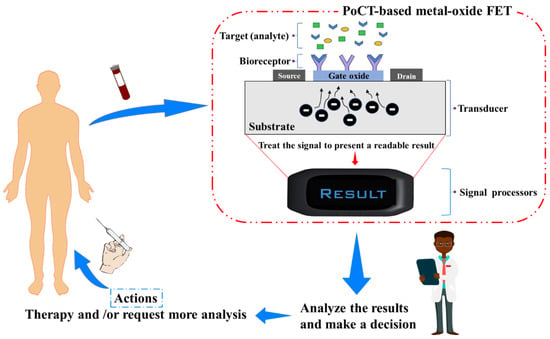
2.2. Operation of Metal-Oxide FET-Based Biosensor
Several types of analytes/biomarkers (e.g., antigen, nucleic acid, virus and virus protein/capsid, bacteria) have been successfully implemented in metal-oxide FET sensors. A FET-based biosensor typically relies on the integration of an ISFET and bioreceptors with suitable binding affinity and specificity to the target analyte. The nature of the target analyte influences the design of the overall assay and detection mechanisms. As with other FET sensors, different classes of bioreceptors can be used, the most common being antibodies and antibody-fragments, enzymes, nucleic acid-based probes, and aptamers. Bioreceptors are typically immobilized on the semiconductor material (the sensing channel) and display biding sites to capture the target analyte(s). The surface potential of the FET sensors and, therefore, the channel conductance changes when these bioreceptors bind with the targets. The channel conductance variation resulting from the presence of the target can be correlated to a sensitivity index by measuring the changes in the drain current. The presence of the target on the sensing channel is typically detected either directly (label-free operation) or via a secondary amplification step. In addition, competitive and displacement affinity assays can also be used, with or without amplification. Label-free assays rely on the intrinsic charges present on the target at the measurement condition [7][35][15,74] or conformational changes induced by its binding and are conceptually easier to design and implement than two-step sandwich assays. However, the issue of the sensor non-specific fouling by biomolecules present in the test matrix typically imposes a limit on the analytical performance. In addition, it is worth mentioning that the Debye length, which governs the extent to which the analytes’ charges affect the FET channel electrical surface characteristics, should also be considered, as it severely limits the direct detection of the analytes in physiological solutions. Various approaches have been proposed to overcome the Debye length effect. For example, an oligonucleotide stem-loop bioreceptor was successfully used for adaptive target recognition in ultrathin In2O3 FETs [36][55]. Another approach modulated the Debye screening length without affecting the FET’s channel surface by fabricating a Meta-Nano-Channel Bio-FET to tune the double-layer shielding electrostatically [37][75]. Signal amplification is typically achieved via an enzymatic reaction, either directly if the bioreceptor is an enzyme or indirectly via a secondary probe conjugated with an enzyme. Direct enzymatic assays are easier to implement than two-step sandwich assays; however, only a limited number of analyte/bioreceptor pairings are available. Biochemical sensing based-FETs can be carried out either in quasi-real time or in steady-state manners. In the former case, a short pulse of gate voltage is applied to enable high-frequency transient measurements while the drain current is continuously monitored, with the sensing channels being immersed in the measuring solution [10][14][38][18,22,49]. Real-time measurements are beneficial for accessing binding kinetic information. However, measuring binding kinetic data ideally requires a fluidic system to deliver the sample and buffer solutions [39][45] and is, therefore, more complex to implement. In the steady measurement, the affinity FET sensors are exposed to the sample containing the target molecules to allow for the binding reaction to take place and eventually reach binding equilibrium or saturation state. Drain currents before and after completion of the assay are acquired, and these measurements are used to extrapolate the concentrations of the target analytes based on a calibration curve [6][40][14,79].3. Development and Integration of Metal-Oxide Nano-FET Biosensor for PoCT
3.1. Fabrication of Nanoscale Metal-Oxide Semiconductors: Vapor-Based Approaches
Scaling down metal-oxide semiconductors into the nanoscale increases their analytical performance due to the comparable size of metal-oxide nanostructures to the targeted molecules [41][82]. Metal-oxide nanostructures, including nanowires (NWs), nanoribbons (NRs), nanobelts, nanorods, and nano-thin films, can be grown using vapor-phase fabrication techniques, which include chemical vapor deposition (CVD) and physical vapor deposition (PVD). Vapor-phase-grown metal-oxide nanostructures. Metal-oxide NWs and nanobelts can be synthesized using vapor processes such as CVD and PVD. As detailed previously, two mechanisms typically govern these fabrication methods: vapor-liquid-solid and vapor-solid mechanisms [42][83]. CVD synthesizes nanostructures (NWs, nanobelts, or nanorods) through chemical reactions in the vapor phase with the assistance of a noble metal catalyst (e.g., Pt, Au). Different metal-oxide NWs have been synthesized through laser ablation CVD procedure [42][43][44][45][83,84,85,86]. Here, NWs are grown in a pre-coated substrate (usually Si/SiO2 substrate) with a catalyst (either a thin film or nanoparticles). During the reaction of the laser beam with the targeted material, clusters or droplets of the targeted material are generated and form the NW backbone based on the catalyst size in the pre-coated substrate. A drawback of using a thin film catalyst is that this produces significantly different NW diameters, so it lacks reproducibility [7][15]. On the other hand, monodisperse metal clusters catalysts allow more control over the NW diameters as the nanocluster catalyst’s size guides the formation of the metal-oxide NWs [46][47][87,88]. Since the synthesis reaction takes place at a high temperature (>770 °C), NWs grown with CVD are crystalline as reported for SnO2 [48][49][50][51][89,90,91,92], In2O3 [45][52][53][54][53,86,93,94], and ZnO [10][55][56][18,44,46]. On the other hand, PVD produces nanostructures by either thermal evaporation or gaseous plasma. In the thermal evaporation process, a high temperature evaporates the material powder under a vacuum. To prepare a functional FET device from metal oxide nanostructures grown in the vapor phase, a patterning/transfer technique is typically required, which aims to transfer the as-synthesized nanostructures to a secondary (receiver) substrate. The patterned semiconductor nanostructures can then be integrated with electrical contacts and isolated using a passivation layer. Shadow masks and conventional photolithography with an etching or lift-off process are mainly used in the patterning step [15][16][57][58][59][23,24,99,100,101]. Conversely, dip-coating is the most used method for transferring metal-oxide FETs to the patterned substrate [60][98]. In this methodology, the as-grown semiconductor materials are transferred from the growth substrate into an organic solvent (usually an alcoholic solution) using ultrasonication. The resulting suspension is then dispensed drop-by-drop onto the secondary substrate. Although there are many reports of successful transfer of CVD/PVD-fabricated metal-oxide nanostructures using dip-coating (e.g., In2O3 [60][61][62][51,98,102], ZnO [10][55][18,44], and SnO2 [49][51][63][90,92,103]), this procedure is limited by the substantial damages occurring in the metal-oxide nanostructures during the ultrasonication step. Alternatively, CVD/PVD-fabricated metal-oxide semiconductors can be transferred with direct contact printing [42][51][83,92]. Vapor-phase thin film deposition techniques. When combined with a patterning process, metal-oxide FET can also be fabricated by top-down vapor-phase thin film deposition approaches. The most commonly used vapor-phase thin film deposition techniques for this purpose include sputtering, atomic layer deposition (ALD), and pulsed laser deposition (PLD). Sputtering is a widely used thin film deposition technique [15][16][57][58][23,24,99,100]. Metal-oxide FET fabrication based on sputtering has several merits, namely (1) relatively low-temperature processing (from room temperature to a few hundred degrees), which makes it readily compatible with a wide range of substrates, for example, flexible plastic substrates [64][65][104,105], silicon/glass substrate, (2) efficient control of the thickness and morphology of the metal thin films by modulating the sputtering conditions (e.g., sputtering power, time, and gas flow rate), and 3) control of the composition of the deposited film by co-sputtering different material targets [65][105]. Metal-oxide thin films can be deposited either from the respective metal-oxide targets in an inert atmosphere or from a pure metal target within an oxidative gas environment, which is typically referred to as reactive sputtering [66][106]. Sputtering of oxide targets in an inert atmosphere is superior due to the simplicity and superior reproducibility of the process, while reactive sputtering is more sensitive to contaminants and process parameters.3.2. Fabrication of Nanoscale Metal-Oxide Semiconductors: Solution-Based Approaches
Most metal-oxide nanostructures/thin films can be synthesized through solution-based routes (e.g., sol-gel [67][68][69][113,114,115], and wet-chemical synthesis [43][68][70][84,114,116]). In this paradigm, the nanoscale metal-oxide elements are subsequently deposited on substrates, for example, using spin coating, spray coating, bar coating, and printing [65][67][71][105,113,117]. When combined with the patterning technique, the solution-based route is cost-effective and more compatible with large-area deposition than vapor-based techniques [67][68][72][113,114,118]. In a typical sol-gel process, a dissolved metal salt precursor is spin-coated or printed directly on a substrate at room temperature. A high-temperature annealing (200–350 °C) step is then used to convert the precursor framework into the desired metal-oxide framework by decomposing and desorbing by-products of the synthesis reaction [45][71][73][86,117,119]. This step determines the metal-oxide FET’s electrical properties. In2O3 thin films [17][73][74][25,119,120], In2O3 nanoribbons [30][72][38,118], and ZnO thin films [69][115] have been successfully fabricated by a sol-gel process with electron mobility μFE > 10 cm2 V−1 s−1, current on/off ratios from 104 to 107, and SS values from 81 mV/decade to 600 mV/decade [17][72][73][74][25,118,119,120]. High-temperature annealing requirement is a drawback of the sol-gel approach. It restricts the substrate material choice as many polymeric substrates cannot tolerate the required high temperature. Therefore, new strategies to lower the annealing temperature are needed to combine this approach with flexible substrates, for example, using novel precursors and/or developing innovative annealing methods [69][71][115,117].3.3. Surface Functionalization of Metal-Oxide-Based FET Sensors
A range of biorecognition approaches, including enzyme/substrate, antibody/antigen interactions, and nucleic acid hybridization, has been exploited to impart selectivity to biosensors for a specific molecular target [75][124]. These bio-affinity recognition methods have been successfully implemented to realize experimental FET biosensors for testing many diseases with high prevalence, such as cancers (e.g., protein biomarkers) [13][67][21,113], cardiovascular diseases (e.g., protein biomarkers) [76][77][125,126], infectious diseases (e.g., nucleotide biomarkers) [29][37], and diabetes (e.g., protein and enzyme biomarkers) [16][24]. An essential step in preparing a nano-FET biosensing device is introducing a molecular bioreceptor with high and specific binding affinities to the target of interest on the surface of the FET. Metal-oxide-based FETs are, therefore, typically functionalized first with a chemical agent to enable covalent immobilization of the specific bioreceptors on their surface. In this regard, organosilanes and phosphonic acids are widely used. Organosilanes covalently bind to many metal-oxides such as In2O3 [30][58][78][79][38,78,100,127], SnO2 [31][39], ZnO [55][44], SiO2 [80][81][128,129], Fe3O4 [82][130], and β-Ga2O3 [83][131]. Presently, 3-aminopropyltriethoxysilane (APTES), 3-mercaptopropyltrimethoxysilane, and 3-(trimethoxysilyl) propyl aldehyde are the most used amongst the organosilanes. Silanization is carried out either in vapor or liquid phases using a mixture of ethanol/water 95%/5% (v/v), or toluene [80][84][85][128,132,133]. Prior to surface functionalization, metal-oxide surfaces are often activated using UV-ozone or oxygen plasma. This activation step generates –OH groups on the surface, facilitating the reaction with the organosilanes. The mechanisms and characteristics of metal-oxide functionalization with organosilanes have been reported in detail elsewhere [80][82][86][87][128,130,134,135]. In the case of APTES, the amine functional groups can be subsequently reacted with a mono or hetero bifunctional linker, such as glutaraldehyde, to introduce reactive groups able to covalently conjugate bioreceptors including DNA probes [88][136], antibodies [13][89][21,137], proteins [89][137], or enzymes [10][18]. After immobilization, unreacted groups (e.g., CHO) are usually blocked, and the surface is passivated toward reducing non-specific adsorption events [84][90][91][132,138,139].4. Tailoring Metal-Oxide Nano-FETs toward Point-of-Care Testing Applications
PoCT as a diagnostic device must be fast time-to-result (ideally in less than an hour), cost-effective, portable, instrument- and technician-free, robust enough in the implementation environments (i.e., weather and shelf-time), and sensitive. Recent advances in metal-oxide nano-FET make it possible to meet the PoCT requirements satisfactorily.