Two-dimensional nanostructures (2DNS) attract tremendous interest and have emerged as potential materials for a variety of applications, including biomolecule sensing, due to their high surface-to-volume ratio, tuneable optical and electronic properties. Advancements in the engineering of 2DNS and associated technologies have opened up new opportunities. Surface-enhanced Raman scattering (SERS) is a rapid, highly sensitive, non-destructive analytical technique with exceptional signal amplification potential. Several structurally and chemically engineered 2DNS with added advantages (e.g., π–π* interaction), over plasmonic SERS substrates, have been developed specifically towards biomolecule sensing in a complex matrix, such as biological fluids.
- surface-enhanced Raman spectroscopy
- chemical enhancement
- two-dimensional nanostructures
1. Introduction
2. 2DNS as SERS Substrates
As mentioned earlier, the Raman signal enhancement by 2DNS is mainly through a charge-transfer mechanism. The electronic structure of the analyte–substrate interface, which is primarily accomplished by the transfer of an electron from the highest occupied molecular orbital (HOMO) to the lowest unoccupied molecular orbital (LUMO), determines the contribution of CM (charge-transfer) to Raman signal amplification. Moreover, the π-interaction facilitates the accumulation of analytes on their surface, which has a significant effect at lower concentrations. On the other hand, 2DNS can anchor the plasmonic nanostructures for better dispersion, i.e., prevention of agglomeration. Here, the SERS enhancement factor (EF), the degree of signal amplification [15], is improved as the essential nano-gaps are created by the well-separated plasmonic nanostructures. Therefore, 2DNS were widely deployed for the later purpose. Figure 2 1 illustrates the use of 2DNS as a SERS substrate and support for nanostructured plasmonic SERS substrates. Table 1 lists representative examples of various 2DNS employed as SERS substrates and support for plasmonic NPs.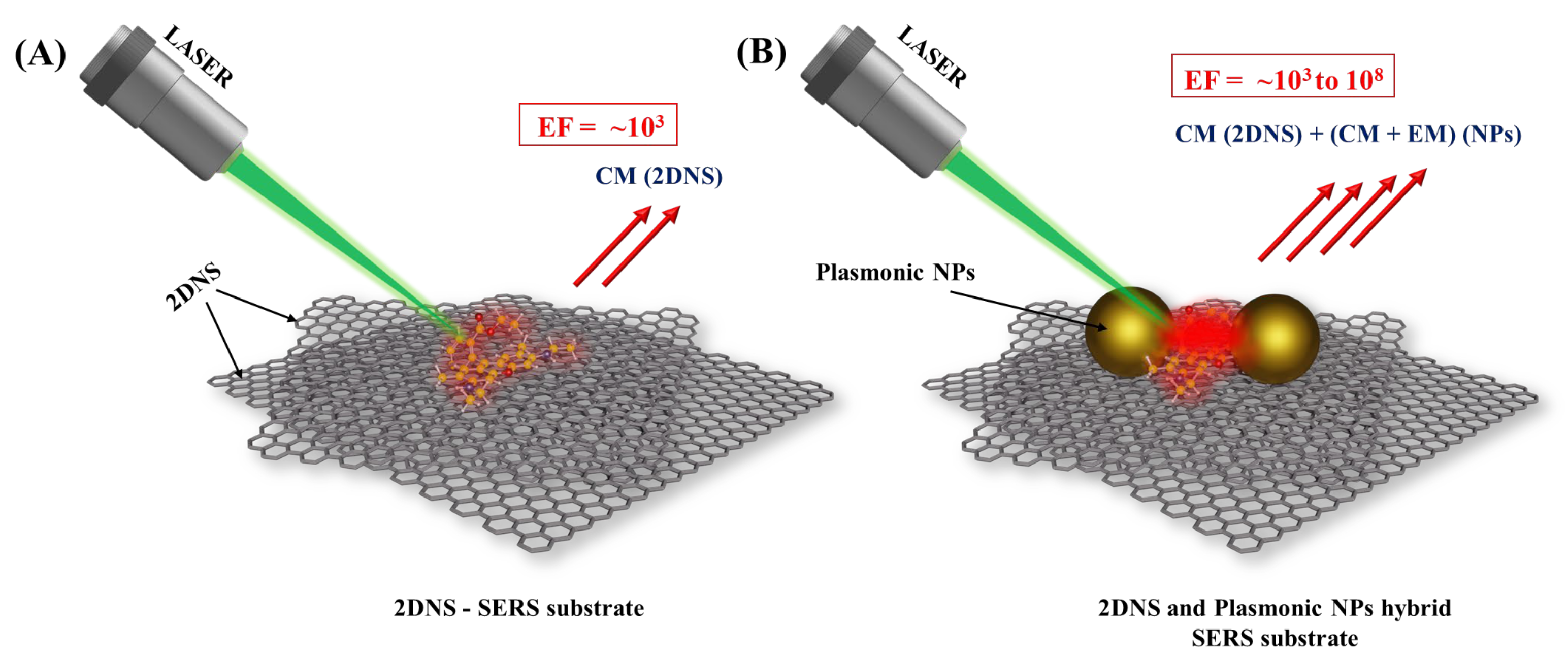
| 2DNS-SERS Substrate |
Probe Molecules | Mechanism | EF | Ref. |
|---|---|---|---|---|
| Graphene | ||||
| Graphene | Rh6G | CM | 1.7 to 5.6 | [32][26] |
| UV/Ozone-GO | RhB, Rh6G, and CV | CM | ∼104 | [33][27] |
| rGO | Rh6G | CM | ∼103 | [34][28] |
| AgNPs/rGO | Rh6G | CM + EM | 2.3 × 10⁸ | [35][29] |
| AuNPs/GO/CW | Rh6G | CM + EM | 1.0 × 10⁶ | [36][30] |
| AgNPs/rGO | RhB | CM + EM | 2.0 × 10⁷ | [37][31] |
| AuNPs/rGO/ | MG | CM + EM | 3.8 × 10³ | [38][32] |
| AgNPs/CVD Graphene | Rh6G | CM + EM | ∼109 | [39][33] |
| TMD | ||||
| TiS2 | Rh6G | CM | 3.2 × 10⁵ | [40][34] |
| 1T-W(MoTe2) | Rh6G | CM | 1.8 × 10⁹ | [41][35] |
| 2H-TaS2 | Rh6G | CM | 1.3 × 10¹⁴ | [42][36] |
| Oxygen incorporated MoS2 | Rh6G | CM | 1.4 × 10⁵ | [43][37] |
| MoTe2 | β-sitosterol | CM | 1.3 × 10⁴ | [44][38] |
| HfTe2 | Rh6G, CV, MB, and MG | CM | ∼106 | [45][39] |
| AuNPs/HfTe2 | MB | CM + EM | 1.7 × 10⁸ | [46][40] |
| AuNWs/MoS2 | Rh6G and MB | CM + EM | ∼107 | [47][41] |
| Black phosphorous (BP) | ||||
| BPQDs/AgNPs/TiO2 | 4-MBA | CM + EM | 2.5 × 10⁵ | [48][42] |
| BP flakes | RhB | CM | ∼106 | [49][43] |
| BP Nanosheets | Rh6G | CM | 6.7 × 10⁷ | [50][44] |
| AgNPs/BP | Interleukin-3 (IL-3) and procalcitonin (PCT) | CM + EM | ∼1014 | [51][45] |
| Nitride | ||||
| Hexagonal Boron Nitride (h-BN) | MG, MB and Rh6G | CM | ∼104 | [52][46] |
| Fluorinated h-BN | Rh6G and CV | CM | ∼108 | [53][47] |
| AgNPs/g-C3N4 | CV | CM + EM | 2.1 × 10⁹ | [54][48] |
| Hydrophilic hydrophobic g-C3N4@Ag | MG | CM + EM | 3.2 × 10⁶ | [55][49] |
| AuNPs/g-C3N4 | Rh6G and Melamine | CM + EM | ∼108 | [56][50] |
| MXenes | ||||
| AuNPs/Mo2C MXene | MB | CM + EM | 2.2 × 10⁴ | [57][51] |
| Ti2N MXene | Rh6G | CM | ∼1012 | [58][52] |
| Ti3C2 | MB | CM | ∼105 | [59][53] |
| Ti3C2 MXene | MB | CM | 2.9 × 10⁶ | [60][54] |
| V4C3 and V2C | Rh6G | CM | ∼105 | [61][55] |
| AuNPs/TiC | Chlorpromazine | CM + EM | ∼109 | [62][56] |
| TiVC | Rh6G | CM | 3.3 × 10¹² | [63][57] |
| Nb2C, Mo2C, Ti2C, V2C, Ti3C2, Mo2TiC2, and Ti3CN | Rh6G | CM | - | [64][58] |
| 2D MOFs/COFs | ||||
| Co-MOFs | Rh6G | CM | - | [65][59] |
| AuNPs/COF-paper | PAHs | CM + EM | 12 to 194 | [66][60] |
2.1. Graphene SERS (GERS) Substrates
Graphene is a single sheet of sp2-bonded carbon atoms in a hexagonal honeycomb lattice. It is the well-known and most explored two-dimensional allotrope of carbon with unusual electronic, optical properties, and high theoretical surface area [67,68][61][62]. The free π-electron, rich in graphene, can make π-interaction with other systems and accumulate on its surface. Consequently, the charge-transfer between the graphene substrate and the adsorbed molecules is enhanced to observe the SERS signal augmentation [69][63]. This phenomenon has been exploited in graphene-enhanced Raman scattering (GERS) for a wide range of applications, including materials development [70][64], energy [71][65] and biomedicine [72,73][66][67].2.2. Nitrides SERS Substrates
The lone-pair electrons in nitrides have an advantage while using them as SERS substrates. A hexagonal lattice made up of boron and nitrogen atoms makes up the equivalent of graphene, known as hexagonal boron nitride (h-BN). Boron nitride possesses a dipole-coupled Raman amplification mechanism, according to a recent investigation [74][68]. Highly sensitive, label-free, and non-destructive biomolecule detection is achieved using h-BN nanostructures [75][69]. However, their wider band gap (~6 eV) requires high excitation energy for a conventional CM signal enhancement, which is not suitable for biological molecules [76][70]. Carbon nitrides are other important 2DNS for Raman signal amplification. Redemann et al. discovered in 1940 that graphitic carbon nitride (g-C3N4) possesses a graphite-like van der Waals layered structure [77][71]. Despite having good physicochemical stability, the poor signal enhancement from pristine g-C3N4 has hindered its use as an independent SERS substrate for sensing applications. However, chemical and structural (e.g., induced disorders to the heptazine chain) modifications may help improve the enhancement factor. Few compound nitride thin films have also been reported as SERS substrates due to their resonant plasmonic characteristics. For example, Shaoli et.al. have prepared titanium nitride (TiN), aluminium nitride (AlN) and titanium-aluminium nitride (TiAlN) thin film SERS substrates with 95% higher signal strength compared to bare glass substrate [78][72]. A highly stable niobium nitride thin film with good uniformity has been prepared by reduction nitridation that enhances the Raman signal of Rh6G by 4 × 103 factor [79][73].2.3. Black Phosphorous (BP) SERS Substrates
Bulk BP was first synthesized in 1914, however, an atomically thin BP 2DNS is realized just recently [80][74]. Compared to red and white phosphorus, BP is the most stable form of elemental phosphorus [81][75]. The 2D zig-zag structure of BP sheets consists of phosphorus atoms with three covalently bonded nearest neighbours, while the sheets are bound together by weak van der Waals forces. These layers can be easily exfoliated into 2D BP nanosheets, since the multi-level quantum chemical calculations indicate an exfoliation energy of −151 meV per atom [82][76]. These wrinkly sheets of honeycomb lattice have armchair and zigzag forms, as in graphene. The layer-dependent band gap, from 0.3 (bulk) to 2.0 eV, of BP allows the use of a wide range of excitation light in the UV, visible and NIR ranges for SERS analysis [83][77]. Interestingly, Lin et al. reported an anisotropic SERS substrate using few-layered BP and ReS2, which exhibited polarization-dependent signal enhancement [84][78]. Therefore, BP nanosheets have recently received great attention for a wide range of applications, particularly in biomedicine, photothermal therapy, photodynamic therapy, drug administration, 3D printing, bio-imaging, and theranostics [85,86,87][79][80][81].2.4. MXenes SERS Substrates
Transition metal carbides, nitrides or carbonitrides make a new class of 2D material, known as MXenes. They typically have a layered structure with (n + 1) layers of M connected by n layers of X in the pattern [MX]n-M, where M is an early transition metal (such as Sc, Ti, Zr, Hf, V, Nb, Ta, Cr or Mo), and X is either carbon or nitrogen. A general formula for these compounds is Mn+1Xn (n = 1–3) [88,89][82][83]. Since its first discovery (Ti3C2) in 2011, MXenes have attracted immense attention in a variety of applications, including energy, environmental and healthcare sectors. The high electrical conductivity of highly metallic MXenes, having unique electronic and optical properties and intense LSPR effect in the visible or near-infrared range, makes them a promising SERS substrate [58][52]. Here, both EM and CM contribute to boosting the Raman signal [90][84]. Their flexibility and hydrophilic nature make functionalization or tagging with Raman reporters, easy.2.5. Transition Metal Dichalcogenide (TMD) SERS Substrates
Compounds with the generalised formula MX2, where M is a transition metal and X is a chalcogen, such as S, Se or Te, make up the family of layered materials known as “transition metal dichalcogenides”. Strong intralayer bonding and weak interlayer binding enable the exfoliation of these van der Waals solids into 2D nanosheets [91][85]. A layer of transition metal sandwiched between two saturated chalcogen layers makes these less reactive 2D TMD layers. The confinement of charge carriers in two dimensions in TMDs dramatically alters their characteristics for a variety of applications [30,92][86][87]. These atomically flat sheets enable effective charge transfer between the probe molecules and substrates through weak contacts, such as π–π* interactions, and make them suitable for chemical Raman signal enhancement [93,94][88][89]. These TMDs are particularly interesting since they facilitate attachment of probed molecules to induce the CM effect [95][90].2.6. Metal Oxide SERS Substrates
Most semiconductors exhibit weak SERS signals due to their large band gaps and lack of surface plasmon resonance. Oxygen incorporation in semiconductors increases the Raman enhancement factor as good as 105 times, probably due to the enhanced charge-transfer from the semiconductor band edges to the adsorbed molecules [96][91]. Metal oxide semiconductors, such as titanium oxide (TiO2), tungsten oxide (WoOx) and molybdenum oxide (MoOx), were recently tested as SERS substrates [43][37]. The surface polarisation effect due to the oxygen defect states boosts the Raman signals in these substrates [97][92]. For instance, few-layered MoO3 nanosheets act as a sensitive SERS substrate, which enhances the Raman signal up to 2.28 × 10⁴ times and makes it capable of detecting 2 × 10⁻⁸ M of an Rh6G molecule [98][93]. Similarly, ultrathin, chemical vapour-deposited MoO2 nanosheets show enhancement of the Raman signal up to 2.1 × 10⁵ and possess excellent reusability and uniformity [99][94]. In both cases, it has been found that the EF further increased by decreasing the thickness of the MoOx nanosheets.2.7. 2D MOFs/COFs SERS Substrates
Metal-Organic Frameworks (MOFs) are crystalline porous materials consisting of metal ions or cluster nodes linked by organic ligands such as carboxylate ligands and other negatively charged ligands [100,101][95][96]. MOFs show excellent SERS performance that is generally attributed to the charge transfer enhancement mechanism [102][97]. Several studies have been carried out to deploy MOFs as SERS substrates. For the first time, Yu et al. reported the Raman signal enhancement of Methyl Orange adsorbed on Matériaux Institut Lavoisier (MIL)-type MOFs [103][98]. Later, several other MOFs, including ZIF-67, Co-TCPP MOFs and Co-MOF-74 were employed directly as SERS substrates, which shows an EF of about 106 for an Rh6G molecule [104][99]. Covalent Organic Frameworks (COFs) are ordered structures built up from organic building blocks via covalent bonds [105][100]. The use of COFs as SERS substrate is still in its infancy, while MOFs gained more popularity because of the plasmonic hybrids. Two-dimensional allotropes of these MOFs and COFs are attracting increasing research attention due to their ultrathin morphology, which offers a high surface-to-volume atom ratio [100][95]. Their high surface area with molecular structure facilitating a π–π* interaction is a critical advantage for their application in SERS substrates.References
- Clark, L.C., Jr.; Lyons, C. Electrode systems for continuous monitoring in cardiovascular surgery. Ann. N. Y. Acad. Sci. 1962, 102, 29–45.
- Naresh, V.; Lee, N. A Review on Biosensors and Recent Development of Nanostructured Materials-Enabled Biosensors. Sensors 2021, 21, 1109.
- Arlett, J.L.; Myers, E.B.; Roukes, M.L. Comparative advantages of mechanical biosensors. Nat. Nanotechnol. 2011, 6, 203–215.
- Murugasenapathi, N.K.; Ghosh, R.; Ramanathan, S.; Ghosh, S.; Chinnappan, A.; Mohamed, S.A.J.; Esther Jebakumari, K.A.; Gopinath, S.C.B.; Ramakrishna, S.; Palanisamy, T. Transistor-Based Biomolecule Sensors: Recent Technological Advancements and Future Prospects. Crit. Rev. Anal. Chem. 2021, 1–22.
- Fleischmann, M.; Hendra, P.J.; McQuillan, A.J. Raman spectra of pyridine adsorbed at a silver electrode. Chem. Phys. Lett. 1974, 26, 163–166.
- Nie, S.; Emory, S.R. Probing Single Molecules and Single Nanoparticles by Surface-Enhanced Raman Scattering. Science 1997, 275, 1102–1106.
- Kneipp, K.; Wang, Y.; Kneipp, H.; Perelman, L.T.; Itzkan, I.; Dasari, R.R.; Feld, M.S. Single molecule detection using surface-enhanced Raman scattering (SERS). Phys. Rev. Lett. 1997, 78, 1667.
- Jeanmaire, D.L.; Van Duyne, R.P. Surface raman spectroelectrochemistry: Part I. Heterocyclic, aromatic, and aliphatic amines adsorbed on the anodized silver electrode. J. Electroanal. Chem. Interfacial Electrochem. 1977, 84, 1–20.
- Albrecht, M.G.; Creighton, J.A. Anomalously intense Raman spectra of pyridine at a silver electrode. J. Am. Chem. Soc. 1977, 99, 5215–5217.
- Moskovits, M. Surface roughness and the enhanced intensity of Raman scattering by molecules adsorbed on metals. J. Chem. Phys. 1978, 69, 4159–4161.
- Managò, S.; Quero, G.; Zito, G.; Tullii, G.; Galeotti, F.; Pisco, M.; De Luca, A.C.; Cusano, A. Tailoring lab-on-fiber SERS optrodes towards biological targets of different sizes. Sens. Actuators B Chem. 2021, 339, 129321.
- Fang, X.; Zheng, C.; Yin, Z.; Wang, Z.; Wang, J.; Liu, J.; Luo, D.; Liu, Y.J. Hierarchically Ordered Silicon Metastructures from Improved Self-Assembly-Based Nanosphere Lithography. ACS Appl. Mater. Interfaces 2020, 12, 12345–12352.
- Pisco, M.; Galeotti, F.; Grisci, G.; Quero, G.; Cusano, A. Self-assembled periodic patterns on the optical fiber tip by microsphere arrays. In Proceedings of the 24th International Conference on Optical Fibre Sensors, Curitiba, Brazil, 28 September–2 October 2015; pp. 165–168.
- Gersten, J.I.; Birke, R.L.; Lombardi, J.R. Theory of enhance i light scattering from molecules adsorbed at the metal-solution interface. Phys. Rev. Lett. 1979, 43, 147.
- Ru, E.L.; Etchegoin, P. Principles of Surface-Enhanced Raman Spectroscopy: And Related Plasmonic Effects; Elsevier Science: Amsterdam, The Netherlands, 2008.
- Langer, J.; Jimenez de Aberasturi, D.; Aizpurua, J.; Alvarez-Puebla, R.A.; Auguié, B.; Baumberg, J.J.; Bazan, G.C.; Bell, S.E.J.; Boisen, A.; Brolo, A.G.; et al. Present and Future of Surface-Enhanced Raman Scattering. ACS Nano 2020, 14, 28–117.
- Lee, S.; Kadam, U.S.; Craig, A.P.; Irudayaraj, J. In Vivo Biodetection using Surface-Enhanced Raman Spectroscopy; CRC Press, Taylor and Francis Group: Boca Raton, FL, USA, 2014.
- Kadam, U.S.; Chavhan, R.L.; Schulz, B.; Irudayaraj, J. Single molecule Raman spectroscopic assay to detect transgene from GM plants. Anal. Biochem. 2017, 532, 60–63.
- Novoselov, K.S.; Geim, A.K.; Morozov, S.V.; Jiang, D.; Zhang, Y.; Dubonos, S.V.; Grigorieva, I.V.; Firsov, A.A. Electric Field Effect in Atomically Thin Carbon Films. Science 2004, 306, 666–669.
- Murali, A.; Lokhande, G.; Deo, K.A.; Brokesh, A.; Gaharwar, A.K. Emerging 2D nanomaterials for biomedical applications. Mater. Today 2021, 50, 276–302.
- Cheng, L.; Wang, X.; Gong, F.; Liu, T.; Liu, Z. 2D Nanomaterials for Cancer Theranostic Applications. Adv. Mater. 2020, 32, 1902333.
- Zhang, J.; Chen, H.; Zhao, M.; Liu, G.; Wu, J. 2D nanomaterials for tissue engineering application. Nano Res. 2020, 13, 2019–2034.
- Karthick Kannan, P.; Shankar, P.; Blackman, C.; Chung, C.H. Recent Advances in 2D Inorganic Nanomaterials for SERS Sensing. Adv. Mater. 2019, 31, 1803432.
- Serafinelli, C.; Fantoni, A.; Alegria, E.C.B.A.; Vieira, M. Plasmonic Metal Nanoparticles Hybridized with 2D Nanomaterials for SERS Detection: A Review. Biosensors 2022, 12, 225.
- Zheng, T.; Zhou, Y.; Feng, E.; Tian, Y. Surface-enhanced Raman Scattering on 2D Nanomaterials: Recent Developments and Applications. Chin. J. Chem. 2021, 39, 745–756.
- Deng, S.; Xu, W.; Wang, J.; Ling, X.; Wu, J.; Xie, L.; Kong, J.; Dresselhaus, M.S.; Zhang, J. Direct measurement of the Raman enhancement factor of rhodamine 6G on graphene under resonant excitation. Nano Res. 2014, 7, 1271–1279.
- Huh, S.; Park, J.; Kim, Y.S.; Kim, K.S.; Hong, B.H.; Nam, J.M. UV/Ozone-Oxidized Large-Scale Graphene Platform with Large Chemical Enhancement in Surface-Enhanced Raman Scattering. ACS Nano 2011, 5, 9799–9806.
- Yu, X.; Cai, H.; Zhang, W.; Li, X.; Pan, N.; Luo, Y.; Wang, X.; Hou, J.G. Tuning Chemical Enhancement of SERS by Controlling the Chemical Reduction of Graphene Oxide Nanosheets. ACS Nano 2011, 5, 952–958.
- Kavitha, C.; Bramhaiah, K.; John, N.S.; Ramachandran, B.E. Low cost, ultra-thin films of reduced graphene oxide–Ag nanoparticle hybrids as SERS based excellent dye sensors. Chem. Phys. Lett. 2015, 629, 81–86.
- Shi, G.; Wang, M.; Zhu, Y.; Shen, L.; Wang, Y.; Ma, W.; Chen, Y.; Li, R. A flexible and stable surface-enhanced Raman scattering (SERS) substrate based on Au nanoparticles/Graphene oxide/Cicada wing array. Opt. Commun. 2018, 412, 28–36.
- Yan, Z.-X.; Zhang, Y.L.; Wang, W.; Fu, X.Y.; Jiang, H.-B.; Liu, Y.Q.; Verma, P.; Kawata, S.; Sun, H.B. Superhydrophobic SERS substrates based on silver-coated reduced graphene oxide gratings prepared by two-beam laser interference. ACS Appl. Mater. Interfaces 2015, 7, 27059–27065.
- Fu, W.L.; Zhen, S.J.; Huang, C.Z. One-pot green synthesis of graphene oxide/gold nanocomposites as SERS substrates for malachite green detection. Analyst 2013, 138, 3075–3081.
- Ayhan, M.E. CVD graphene-based flexible and transparent SERS substrate towards L-tyrosine detection. Microelectron. Eng. 2021, 241, 111546.
- Weng, C.; Luo, Y.; Wang, B.; Shi, J.; Gao, L.; Cao, Z.; Duan, G.J. Layer-dependent SERS enhancement of TiS2 prepared by simple electrochemical intercalation. J. Mater. Chem. C 2020, 8, 14138–14145.
- Tao, L.; Chen, K.; Chen, Z.; Cong, C.; Qiu, C.; Chen, J.; Wang, X.; Chen, H.; Yu, T.; Xie, W.; et al. 1T′ Transition Metal Telluride Atomic Layers for Plasmon-Free SERS at Femtomolar Levels. J. Am. Chem. Soc. 2018, 140, 8696–8704.
- Ekoya, B.G.; Shan, Y.; Cai, Y.; Okombi, N.I.; Yue, X.; Xu, M.; Cong, C.; Hu, L.; Qiu, Z.-J.; Liu, R. 2H Tantalum Disulfide Nanosheets as Substrates for Ultrasensitive SERS-Based Sensing. ACS Appl. Nano Mater. 2022, 5, 8913–8920.
- Zheng, Z.; Cong, S.; Gong, W.; Xuan, J.; Li, G.; Lu, W.; Geng, F.; Zhao, Z. Semiconductor SERS enhancement enabled by oxygen incorporation. Nat. Commun. 2017, 8, 1993.
- Fraser, J.P.; Postnikov, P.; Miliutina, E.; Kolska, Z.; Valiev, R.; Švorčík, V.; Lyutakov, O.; Ganin, A.Y.; Guselnikova, O. Application of a 2D Molybdenum Telluride in SERS Detection of Biorelevant Molecules. ACS Appl. Mater. Interfaces 2020, 12, 47774–47783.
- Li, Y.; Chen, H.; Guo, Y.; Wang, K.; Zhang, Y.; Lan, P.; Guo, J.; Zhang, W.; Zhong, H.; Guo, Z.; et al. Lamellar hafnium ditelluride as an ultrasensitive surface-enhanced Raman scattering platform for label-free detection of uric acid. Photonics Res. 2021, 9, 1039–1047.
- Li, Y.; Guo, Y.; Ye, B.; Zhuang, Z.; Lan, P.; Zhang, Y.; Zhong, H.; Liu, H.; Guo, Z.; Liu, Z. Rapid label-free SERS detection of foodborne pathogenic bacteria based on hafnium ditelluride-Au nanocomposites. J. Innov. Opt. Heal. Sci. 2020, 13, 2041004.
- Yuan, H.; Yu, S.; Kim, M.; Lee, J.-E.; Kang, H.; Jang, D.; Ramasamy, M.S.; Kim, D.H. Dopamine-mediated self-assembled anisotropic Au nanoworms conjugated with MoS2 nanosheets for SERS-based sensing. Sens. Actuators B Chem. 2022, 371, 132453.
- Guo, J.; Ding, C.; Gan, W.; Chen, P.; Zhang, M.; Sun, Z. Fabrication of black phosphorous quantum dots and Ag nanoparticles co-sensitized TiO2 nanorod arrays as powerful SERS substrate. J. Alloy. Compd. 2022, 918, 165621.
- Kundu, A.; Rani, R.; Hazra, K.S. Controlled nanofabrication of metal-free SERS substrate on few layered black phosphorus by low power focused laser irradiation. Nanoscale 2019, 11, 16245–16252.
- Lin, C.; Liang, S.; Peng, Y.; Long, L.; Li, Y.; Huang, Z.; Long, N.V.; Luo, X.; Liu, J.; Li, Z.; et al. Visualized SERS Imaging of Single Molecule by Ag/Black Phosphorus Nanosheets. Nanomicro Lett. 2022, 14, 75.
- Kundu, A.; Rani, R.; Ahmad, A.; Kumar, A.; Raturi, M.; Gupta, T.; Khan, R.; Hazra, K.S. Ultrasensitive and label-free detection of prognostic and diagnostic biomarkers of sepsis on a AgNP-laden black phosphorous-based SERS platform. Sensors Diagn. 2022, 1, 449–459.
- Basu, N.; Satya Bharathi, M.S.; Sharma, M.; Yadav, K.; Parmar, A.S.; Soma, V.R.; Lahiri, J. Large Area Few-Layer Hexagonal Boron Nitride as a Raman Enhancement Material. Nanomaterials 2021, 11, 622.
- Ahmad, A.u.; Abbas, Q.; Ali, S.; Fakhar-e-alam, M.; Farooq, Z.; Farid, A.; Abbas, A.; Javid, M.; Muhammad Afzal, A.; Umair Arshad, H.M.; et al. Fluorinated hexagonal boron nitride as a spacer with silver nanorods for surface enhanced Raman spectroscopy analysis. Ceram. Int. 2021, 47, 6528–6534.
- Jiang, J.; Zou, J.; Wee, A.T.S.; Zhang, W. Use of Single-Layer g-C3N4/Ag Hybrids for Surface-Enhanced Raman Scattering (SERS). Sci. Rep. 2016, 6, 34599.
- Jiang, Y.; Sun, H.; Gu, C.; Zhang, Y.; Jiang, T. A hydrophilic–hydrophobic graphitic carbon hybrid substrate for recyclable surface-enhanced Raman scattering-based detection without the coffee-ring effect. Analyst 2021, 146, 5923–5933.
- Tiwari, M.; Singh, A.; Thakur, D.; Pattanayek, S.K. Graphitic carbon nitride-based concoction for detection of melamine and R6G using surface-enhanced Raman scattering. Carbon 2022, 197, 311–323.
- Rajput, P.; Devi, P. In-situ synthesized gold nanoparticles modified Mo2C MXene for surface enhanced Raman scattering. Graphene 2D Mater. 2022, 7, 107–117.
- Soundiraraju, B.; George, B.K. Two-Dimensional Titanium Nitride (Ti2N) MXene: Synthesis, Characterization, and Potential Application as Surface-Enhanced Raman Scattering Substrate. ACS Nano 2017, 11, 8892–8900.
- Satheeshkumar, E.; Makaryan, T.; Melikyan, A.; Minassian, H.; Gogotsi, Y.; Yoshimura, M. One-step Solution Processing of Ag, Au and Hybrids for SERS. Sci. Rep. 2016, 6, 32049.
- Peng, Y.; Cai, P.; Yang, L.; Liu, Y.; Zhu, L.; Zhang, Q.; Liu, J.; Huang, Z.; Yang, Y. Theoretical and Experimental Studies of Ti3C2 MXene for Surface-Enhanced Raman Spectroscopy-Based Sensing. ACS Omega 2020, 5, 26486–26496.
- Lan, L.; Fan, X.; Yu, S.; Gao, J.; Zhao, C.; Hao, Q.; Qiu, T. Flexible Two-Dimensional Vanadium Carbide MXene-Based Membranes with Ultra-Rapid Molecular Enrichment for Surface-Enhanced Raman Scattering. ACS Appl. Mater. Interfaces 2022, 14, 40427–40436.
- Barveen, N.R.; Wang, T.-J.; Chang, Y.H. A photochemical approach to anchor Au NPs on MXene as a prominent SERS substrate for ultrasensitive detection of chlorpromazine. Microchim. Acta 2021, 189, 16.
- He, Z.; Rong, T.; Li, Y.; Ma, J.; Li, Q.; Wu, F.; Wang, Y.; Wang, F. Two-Dimensional TiVC Solid-Solution MXene as Surface-Enhanced Raman Scattering Substrate. ACS Nano 2022, 16, 4072–4083.
- Shevchuk, K.; Sarycheva, A.; Gogotsi, Y. Evaluation of two-dimensional transition-metal carbides and carbonitrides (MXenes) for SERS substrates. MRS Bull. 2022, 47, 545–554.
- Sun, H.; Gong, W.; Cong, S.; Liu, C.; Song, G.; Lu, W.; Zhao, Z. Ultrathin Two-Dimensional Metal–Organic Framework Nanosheets with Activated Ligand-Cluster Units for Enhanced SERS. ACS Appl. Mater. Interfaces 2022, 14, 2326–2334.
- Zhang, G.-L.; Zhang, M.; Shi, Q.; Jiang, Z.; Tong, L.; Chen, Z.; Tang, B. In Situ Construction of COF-Based Paper Serving as a Plasmonic Substrate for Enhanced PSI-MS Detection of Polycyclic Aromatic Hydrocarbons. ACS Appl. Mater. Interfaces 2021, 13, 43438–43448.
- Yang, G.; Li, L.; Lee, W.B.; Ng, M.C. Structure of graphene and its disorders: A review. Sci. Technol. Adv. Mater. 2018, 19, 613–648.
- Xu, W.; Paidi, S.K.; Qin, Z.; Huang, Q.; Yu, C.-H.; Pagaduan, J.V.; Buehler, M.J.; Barman, I.; Gracias, D.H. Self-folding hybrid graphene skin for 3D biosensing. Nano Lett. 2018, 19, 1409–1417.
- Ding, S.-Y.; You, E.-M.; Tian, Z.Q.; Moskovits, M. Electromagnetic theories of surface-enhanced Raman spectroscopy. Chem. Soc. Rev. 2017, 46, 4042–4076.
- Li, D.; Kaner, R.B. Graphene-based materials. Science 2008, 320, 1170–1171.
- Sun, Y.; Wu, Q.; Shi, G. Graphene based new energy materials. Energy Environ. Sci. 2011, 4, 1113–1132.
- Kim, T.-H.; Lee, D.; Choi, J.-W. Bioelectronics. Live cell biosensing platforms using graphene-based hybrid nanomaterials. Biosens. Bioelectron. 2017, 94, 485–499.
- Huang, S.; Pandey, R.; Barman, I.; Kong, J.; Dresselhaus, M. Raman enhancement of blood constituent proteins using graphene. ACS Photon. 2018, 5, 2978–2982.
- Geng, Z.-Q.; Xu, D.; Song, Y.; Wang, W.-P.; Li, Y.-P.; Han, C.-Q.; Yang, G.-H.; Qu, L.-L.; Ajayan, P.M. Sensitive label-free detection of bilirubin in blood using boron nitride-modified nanorod arrays as SERS substrates. Sens. Actuators B Chem. 2021, 334, 129634.
- Cai, Q.; Li, L.H.; Yu, Y.; Liu, Y.; Huang, S.; Chen, Y.; Watanabe, K.; Taniguchi, T. Boron nitride nanosheets as improved and reusable substrates for gold nanoparticles enabled surface enhanced Raman spectroscopy. Phys. Chem. Chem. Phys. 2015, 17, 7761–7766.
- Li, L.H.; Cervenka, J.; Watanabe, K.; Taniguchi, T.; Chen, Y. Strong oxidation resistance of atomically thin boron nitride nanosheets. ACS Nano 2014, 8, 1457–1462.
- Huang, D.; Yan, X.; Yan, M.; Zeng, G.; Zhou, C.; Wan, J.; Cheng, M.; Xue, W. Graphitic carbon nitride-based heterojunction photoactive nanocomposites: Applications and mechanism insight. ACS Appl. Mater. Interfaces 2018, 10, 21035–21055.
- Zhu, S.; Xiao, L.; Cortie, M.B. Surface enhanced Raman spectroscopy on metal nitride thin films. Vib. Spectrosc. 2016, 85, 146–148.
- Wang, X.; Wu, Z.; Wei, Y.; Wu, M.; Chen, Y.; Hu, S.; Pei, Y.; Cui, Y.; Lv, D.; Chen, Y.; et al. Synthesis and SERS activity of niobium nitride thin films via reduction nitridation of sol-gel derived films. Opt. Mater. 2022, 123, 111879.
- Li, L.; Yu, Y.; Ye, G.J.; Ge, Q.; Ou, X.; Wu, H.; Feng, D.; Chen, X.H.; Zhang, Y.J. Black phosphorus field-effect transistors. Nat. Nanotechnol. 2014, 9, 372–377.
- Zhang, Y.; Zheng, Y.; Rui, K.; Hng, H.H.; Hippalgaonkar, K.; Xu, J.; Sun, W.; Zhu, J.; Yan, Q.; Huang, W. 2D black phosphorus for energy storage and thermoelectric applications. Small 2017, 13, 1700661.
- Sansone, G.; Maschio, L.; Usvyat, D.; Schütz, M.; Karttunen, A. Toward an Accurate Estimate of the Exfoliation Energy of Black Phosphorus: A Periodic Quantum Chemical Approach. J. Phys. Chem. Lett. 2016, 7, 131–136.
- Luo, Z.-C.; Liu, M.; Guo, Z.-N.; Jiang, X.-F.; Luo, A.-P.; Zhao, C.-J.; Yu, X.-F.; Xu, W.-C.; Zhang, H. Microfiber-based few-layer black phosphorus saturable absorber for ultra-fast fiber laser. Opt. Express 2015, 23, 20030–20039.
- Lin, J.; Liang, L.; Ling, X.; Zhang, S.; Mao, N.; Zhang, N.; Sumpter, B.G.; Meunier, V.; Tong, L.; Zhang, J. Enhanced Raman Scattering on In-Plane Anisotropic Layered Materials. J. Am. Chem. Soc. 2015, 137, 15511–15517.
- Choi, J.R.; Yong, K.W.; Choi, J.Y.; Nilghaz, A.; Lin, Y.; Xu, J.; Lu, X.J. Black phosphorus and its biomedical applications. Theranostics 2018, 8, 1005.
- Gui, R.; Jin, H.; Wang, Z.; Li, J.J. Black phosphorus quantum dots: Synthesis, properties, functionalized modification and applications. Chem Soc Rev. 2018, 47, 6795–6823.
- Zhou, Y.; Qiao, H.; Huang, Z.; Ma, Q.; Liu, F.; Liao, G.; Luo, S.; Zhong, J.; Qi, X. Black Phosphorus Quantum Dots as Hole Capturers in Group-VA Monoelemental Heterostructures for the Application of High-Performance Flexible Photodetectors. ACS Sustain. Chem. Eng. 2021, 9, 14918–14926.
- Naguib, M.; Kurtoglu, M.; Presser, V.; Lu, J.; Niu, J.; Heon, M.; Hultman, L.; Gogotsi, Y.; Barsoum, M.W. Two-dimensional nanocrystals produced by exfoliation of Ti3AlC2. Adv. Mater. 2011, 23, 4248–4253.
- Anasori, B.; Lukatskaya, M.R.; Gogotsi, Y. 2D metal carbides and nitrides (MXenes) for energy storage. Nat. Rev. Mater. 2017, 2, 16098.
- Sarycheva, A.; Makaryan, T.; Maleski, K.; Satheeshkumar, E.; Melikyan, A.; Minassian, H.; Yoshimura, M.; Gogotsi, Y. Two-dimensional titanium carbide (MXene) as surface-enhanced Raman scattering substrate. J. Phys. Chem. C 2017, 121, 19983–19988.
- Chhowalla, M.; Liu, Z.; Zhang, H. Two-dimensional transition metal dichalcogenide (TMD) nanosheets. Chem. Soc. Rev. 2015, 44, 2584–2586.
- Chen, M.; Liu, D.; Du, X.; Lo, K.H.; Wang, S.; Zhou, B.; Pan, H. 2D materials: Excellent substrates for surface-enhanced Raman scattering (SERS) in chemical sensing and biosensing. TrAC Trends Anal. Chem. 2020, 130, 115983.
- Ghopry, S.A.; Alamri, M.; Goul, R.; Cook, B.; Sadeghi, S.M.; Gutha, R.R.; Sakidja, R.; Wu, J.Z. Au Nanoparticle/WS2 Nanodome/Graphene van der Waals heterostructure substrates for surface-enhanced Raman spectroscopy. ACS Appl. Nano Mater. 2020, 3, 2354–2363.
- Geim, A.K.; Novoselov, K.S. The rise of graphene. Nat. Mater. 2007, 6, 183–191.
- Geim, A.K.; Grigorieva, I.V. Van der Waals heterostructures. Nature 2013, 499, 419–425.
- Ling, X.; Fang, W.; Lee, Y.-H.; Araujo, P.T.; Zhang, X.; Rodriguez-Nieva, J.F.; Lin, Y.; Zhang, J.; Kong, J.; Dresselhaus, M.S. Raman enhancement effect on two-dimensional layered materials: Graphene, h-BN and MoS2. Nano Lett. 2014, 14, 3033–3040.
- Cong, S.; Yuan, Y.; Chen, Z.; Hou, J.; Yang, M.; Su, Y.; Zhang, Y.; Li, L.; Li, Q.; Geng, F.; et al. Noble metal-comparable SERS enhancement from semiconducting metal oxides by making oxygen vacancies. Nat. Commun. 2015, 6, 7800.
- Wu, H.; Wang, H.; Li, G. Metal oxide semiconductor SERS-active substrates by defect engineering. Analyst 2017, 142, 326–335.
- He, R.; Lai, H.; Wang, S.; Chen, T.; Xie, F.; Chen, Q.; Liu, P.; Chen, J.; Xie, W. Few-layered vdW MoO3 for sensitive, uniform and stable SERS applications. Appl. Surf. Sci. 2020, 507, 145116.
- Wu, H.; Zhou, X.; Li, J.; Li, X.; Li, B.; Fei, W.; Zhou, J.; Yin, J.; Guo, W. Ultrathin Molybdenum Dioxide Nanosheets as Uniform and Reusable Surface-Enhanced Raman Spectroscopy Substrates with High Sensitivity. Small 2018, 14, 1802276.
- Zhao, M.; Huang, Y.; Peng, Y.; Huang, Z.; Ma, Q.; Zhang, H. Two-dimensional metal–organic framework nanosheets: Synthesis and applications. Chem. Soc. Rev. 2018, 47, 6267–6295.
- Carrasco, S. Metal-Organic Frameworks for the Development of Biosensors: A Current Overview. Biosensors 2018, 8, 92.
- Sun, H.; Yu, B.; Pan, X.; Zhu, X.; Liu, Z. Recent progress in metal–organic frameworks-based materials toward surface-enhanced Raman spectroscopy. Appl. Spectrosc. Rev. 2022, 57, 513–528.
- Yu, T.-H.; Ho, C.-H.; Wu, C.-Y.; Chien, C.-H.; Lin, C.-H.; Lee, S. Metal–organic frameworks: A novel SERS substrate. J. Raman Spectrosc. 2013, 44, 1506–1511.
- Sun, H.; Cong, S.; Zheng, Z.; Wang, Z.; Chen, Z.; Zhao, Z. Metal–Organic Frameworks as Surface Enhanced Raman Scattering Substrates with High Tailorability. J. Am. Chem. Soc. 2019, 141, 870–878.
- Geng, K.; He, T.; Liu, R.; Dalapati, S.; Tan, K.T.; Li, Z.; Tao, S.; Gong, Y.; Jiang, Q.; Jiang, D. Covalent Organic Frameworks: Design, Synthesis, and Functions. Chem. Rev. 2020, 120, 8814–8933.