2. 2DNS as SERS Substrates
As mentioned earlier, the Raman signal enhancement by 2DNS is mainly through a charge-transfer mechanism. The electronic structure of the analyte–substrate interface, which is primarily accomplished by the transfer of an electron from the highest occupied molecular orbital (HOMO) to the lowest unoccupied molecular orbital (LUMO), determines the contribution of CM (charge-transfer) to Raman signal amplification. Moreover, the π-interaction facilitates the accumulation of analytes on their surface, which has a significant effect at lower concentrations. On the other hand, 2DNS can anchor the plasmonic nanostructures for better dispersion, i.e., prevention of agglomeration. Here, the SERS enhancement factor (EF), the degree of signal amplification
[15], is improved as the essential nano-gaps are created by the well-separated plasmonic nanostructures. Therefore, 2DNS were widely deployed for the later purpose.
Figure 1 2 illustrates the use of 2DNS as a SERS substrate and support for nanostructured plasmonic SERS substrates.
Table 1 lists representative examples of various 2DNS employed as SERS substrates and support for plasmonic NPs.
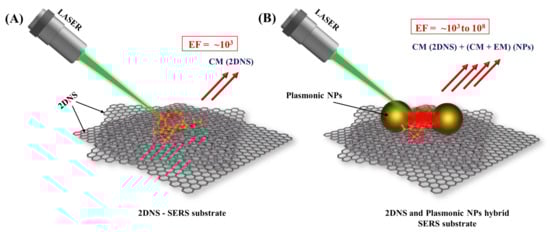
Figure 12. Schematic illustration of (A) 2DNS SERS substrate rendering enhancement through CM and (B) 2DNS as support for plasmonic NPs SERS substrate that enhances Raman signal by both CM (from 2DNS and NPs) and EM (from NPs).
Table 1. Representative examples of 2DNS-SERS substrates (Rhodamine 6G (Rh6G); Rhodamine B (RhB); Malachite Green (MG); Methylene Blue (MB); Crystal Violet (CV).
2.1. Graphene SERS (GERS) Substrates
Graphene is a single sheet of sp
2-bonded carbon atoms in a hexagonal honeycomb lattice. It is the well-known and most explored two-dimensional allotrope of carbon with unusual electronic, optical properties, and high theoretical surface area
[61][62][67,68]. The free π-electron, rich in graphene, can make π-interaction with other systems and accumulate on its surface. Consequently, the charge-transfer between the graphene substrate and the adsorbed molecules is enhanced to observe the SERS signal augmentation
[63][69]. This phenomenon has been exploited in graphene-enhanced Raman scattering (GERS) for a wide range of applications, including materials development
[64][70], energy
[65][71] and biomedicine
[66][67][72,73].
2.2. Nitrides SERS Substrates
The lone-pair electrons in nitrides have an advantage while using them as SERS substrates. A hexagonal lattice made up of boron and nitrogen atoms makes up the equivalent of graphene, known as hexagonal boron nitride (h-BN). Boron nitride possesses a dipole-coupled Raman amplification mechanism, according to a recent investigation
[68][74]. Highly sensitive, label-free, and non-destructive biomolecule detection is achieved using h-BN nanostructures
[69][75]. However, their wider band gap (~6 eV) requires high excitation energy for a conventional CM signal enhancement, which is not suitable for biological molecules
[70][76].
Carbon nitrides are other important 2DNS for Raman signal amplification. Redemann et al. discovered in 1940 that graphitic carbon nitride (g-C
3N
4) possesses a graphite-like van der Waals layered structure
[71][77]. Despite having good physicochemical stability, the poor signal enhancement from pristine g-C
3N
4 has hindered its use as an independent SERS substrate for sensing applications. However, chemical and structural (e.g., induced disorders to the heptazine chain) modifications may help improve the enhancement factor.
Few compound nitride thin films have also been reported as SERS substrates due to their resonant plasmonic characteristics. For example, Shaoli et.al. have prepared titanium nitride (TiN), aluminium nitride (AlN) and titanium-aluminium nitride (TiAlN) thin film SERS substrates with 95% higher signal strength compared to bare glass substrate
[72][78]. A highly stable niobium nitride thin film with good uniformity has been prepared by reduction nitridation that enhances the Raman signal of Rh6G by 4 × 10
3 factor
[73][79].
2.3. Black Phosphorous (BP) SERS Substrates
Bulk BP was first synthesized in 1914, however, an atomically thin BP 2DNS is realized just recently
[74][80]. Compared to red and white phosphorus, BP is the most stable form of elemental phosphorus
[75][81]. The 2D zig-zag structure of BP sheets consists of phosphorus atoms with three covalently bonded nearest neighbours, while the sheets are bound together by weak van der Waals forces. These layers can be easily exfoliated into 2D BP nanosheets, since the multi-level quantum chemical calculations indicate an exfoliation energy of −151 meV per atom
[76][82]. These wrinkly sheets of honeycomb lattice have armchair and zigzag forms, as in graphene. The layer-dependent band gap, from 0.3 (bulk) to 2.0 eV, of BP allows the use of a wide range of excitation light in the UV, visible and NIR ranges for SERS analysis
[77][83]. Interestingly, Lin et al. reported an anisotropic SERS substrate using few-layered BP and ReS
2, which exhibited polarization-dependent signal enhancement
[78][84]. Therefore, BP nanosheets have recently received great attention for a wide range of applications, particularly in biomedicine, photothermal therapy, photodynamic therapy, drug administration, 3D printing, bio-imaging, and theranostics
[79][80][81][85,86,87].
2.4. MXenes SERS Substrates
Transition metal carbides, nitrides or carbonitrides make a new class of 2D material, known as MXenes. They typically have a layered structure with (
n + 1) layers of
M connected by
n layers of
X in the pattern
[MX]n-M, where
M is an early transition metal (such as Sc, Ti, Zr, Hf, V, Nb, Ta, Cr or Mo), and
X is either carbon or nitrogen. A general formula for these compounds is
Mn+1Xn (
n = 1–3)
[82][83][88,89]. Since its first discovery (Ti
3C
2) in 2011, MXenes have attracted immense attention in a variety of applications, including energy, environmental and healthcare sectors. The high electrical conductivity of highly metallic MXenes, having unique electronic and optical properties and intense LSPR effect in the visible or near-infrared range, makes them a promising SERS substrate
[52][58]. Here, both EM and CM contribute to boosting the Raman signal
[84][90]. Their flexibility and hydrophilic nature make functionalization or tagging with Raman reporters, easy.
2.5. Transition Metal Dichalcogenide (TMD) SERS Substrates
Compounds with the generalised formula
MX2, where
M is a transition metal and
X is a chalcogen, such as S, Se or Te, make up the family of layered materials known as “transition metal dichalcogenides”. Strong intralayer bonding and weak interlayer binding enable the exfoliation of these van der Waals solids into 2D nanosheets
[85][91]. A layer of transition metal sandwiched between two saturated chalcogen layers makes these less reactive 2D TMD layers. The confinement of charge carriers in two dimensions in TMDs dramatically alters their characteristics for a variety of applications
[86][87][30,92]. These atomically flat sheets enable effective charge transfer between the probe molecules and substrates through weak contacts, such as π–π* interactions, and make them suitable for chemical Raman signal enhancement
[88][89][93,94]. These TMDs are particularly interesting since they facilitate attachment of probed molecules to induce the CM effect
[90][95].
2.6. Metal Oxide SERS Substrates
Most semiconductors exhibit weak SERS signals due to their large band gaps and lack of surface plasmon resonance. Oxygen incorporation in semiconductors increases the Raman enhancement factor as good as 10
5 times, probably due to the enhanced charge-transfer from the semiconductor band edges to the adsorbed molecules
[91][96]. Metal oxide semiconductors, such as titanium oxide (TiO
2), tungsten oxide (WoOx) and molybdenum oxide (MoOx), were recently tested as SERS substrates
[37][43]. The surface polarisation effect due to the oxygen defect states boosts the Raman signals in these substrates
[92][97]. For instance, few-layered MoO
3 nanosheets act as a sensitive SERS substrate, which enhances the Raman signal up to 2.28 × 10
4 times and makes it capable of detecting 2 × 10
−8 M of an Rh6G molecule
[93][98]. Similarly, ultrathin, chemical vapour-deposited MoO
2 nanosheets show enhancement of the Raman signal up to 2.1 × 10
5 and possess excellent reusability and uniformity
[94][99]. In both cases, it has been found that the EF further increased by decreasing the thickness of the MoO
x nanosheets.
2.7. 2D MOFs/COFs SERS Substrates
Metal-Organic Frameworks (MOFs) are crystalline porous materials consisting of metal ions or cluster nodes linked by organic ligands such as carboxylate ligands and other negatively charged ligands
[95][96][100,101]. MOFs show excellent SERS performance that is generally attributed to the charge transfer enhancement mechanism
[97][102]. Several studies have been carried out to deploy MOFs as SERS substrates. For the first time, Yu et al. reported the Raman signal enhancement of Methyl Orange adsorbed on Matériaux Institut Lavoisier (MIL)-type MOFs
[98][103]. Later, several other MOFs, including ZIF-67, Co-TCPP MOFs and Co-MOF-74 were employed directly as SERS substrates, which shows an EF of about 10
6 for an Rh6G molecule
[99][104]. Covalent Organic Frameworks (COFs) are ordered structures built up from organic building blocks via covalent bonds
[100][105]. The use of COFs as SERS substrate is still in its infancy, while MOFs gained more popularity because of the plasmonic hybrids. Two-dimensional allotropes of these MOFs and COFs are attracting increasing research attention due to their ultrathin morphology, which offers a high surface-to-volume atom ratio
[95][100]. Their high surface area with molecular structure facilitating a π–π* interaction is a critical advantage for their application in SERS substrates.