Your browser does not fully support modern features. Please upgrade for a smoother experience.
Please note this is a comparison between Version 1 by Adnan Alhaj Hasan and Version 4 by Dean Liu.
With the growth of the radioelectronic complexity and the demand for cutting edge devices, the need to protect them and increase their reliability is also rising. There are many methods to provide this. Modal reservation is one of the most effective, reliable, and least complicated methods used nowadays. Using this method in tracing and mounting of printed circuit boards can guarantee both electromagnetic compatibility (by using modal filtering) and reliability (by using the cold redundancy) of the final electronic device.
- electromagnetic compatibility
- redundancy
- modal reservation
1. Introduction
A highly reliable system requires that engineers should increase component reliability (for example, changing the component material) or apply redundancy methods using the existing resources without violating the system’s cost, weight, and volume constraints [1][2][1,2]. The second choice is preferable because of its simplicity [3] and its first implementation is referred in the literature to the work conducted in 1956 [4]. Redundancy is likely to be applied in critical systems where uninterrupted operation is required, and the maintenance is difficult and expensive, for example in the case of onboard radioelectronic systems. In this case, the mission time of communication satellites may last for more than 10 years [5]. Systems or subsystems may be reserved in active or inactive mode with lower failure rates, since the reserved components will be in standby mode until failure [6]. In addition, those reservation types can be combined and divided into sub-types: parallel and k-out-of-n active reservation types, and the cold, hot, and warm standby reservation types [7][8][7,8]. Reservation can be employed not only to improve a system’s reliability, but also its efficiency [9]. Moreover, reservation is considered to be a quick solution to achieve any desirable level of reliability in the early design stage [10]. Since reservation can be performed in different forms, the optimized design of the system can be obtained by reaching the balance between the system’s cost and reliability. Several works have been devoted to developing mathematical models to determine system reliability [11][12][13][11,12,13], even in real-time applications [14]. Reservation in all its types has been used in different fields. It has been employed in information protection [15], memristive devices [16], and in neural networks [17]. It has even been employed in nanotechnology which has a high defect rate [18][19][18,19]. Moreover, this technique is also popular in space [20][21][20,21] and aviation [22] applications, and in modern systems related to unmanned aerial vehicles, for example to protect their datalink [23]. Reservation is also used in communication applications [24]. The printed circuit board (PCB) failures can lead to critical problems and have various causes such as aging, heating, and insulting [25]. To manage these failures, reservation should be commonly used in PCB design. Several works have described the use of this technique for this purpose [26][27][26,27]. However, reservation is not always useful, for example, if the system is not designed to deal with artificial or natural electromagnetic interference (EMI), that can be caused by reservation itself [28]. Thus, ensuring electromagnetic compatibility (EMC) in PCB design, even when the design includes reservation, is unavoidable when dealing with electromagnetic disturbances [29][30][29,30]. Some researchers have tried to increase the reliability of PCBs with reservation taking EMI into account [31], but there was no comprehensive way to do this [32][33][32,33]. In general, one can say that all traditional ways to deal with EMI consequences are not highly effective especially against ultrashort pulses (USP) [34].
Modal reservation (MR) , considered in this work, is a method that can both improve the reliability of radioelectronic devices using cold standby reservation and ensures their EMC by using the so-called technique of modal filtering [35]. Modal filtering is used to protect radioelectronic devices from USPs; it is also used as a method to detect and diagnose contactless electrical connections in hidden walls [36]. MR can also be used in different applications. However, the most important application of this method is in critical and onboard radioelectronic devices. For example, MR is used to increase noise immunity of digital signal processing units [37] and power systems [38] of spacecraft autonomous navigation systems. This method has several types: based on the multiplicity of redundancy (single, dual, triple, … n-tuple) [39], based on the structure symmetry (symmetrical and asymmetrical) [40], and based on the target item (PCB trace or components, cable, dielectric) [41]. Most of these types have been extensively investigated in terms of conducted emissions. To fully explain the mechanism of this method and interpret its consequences, it is also necessary to study its characteristics in terms of radiated emissions (RE). This has been reflected in only a few works [42][43][44][45][42,43,44,45], where such investigations were performed using only the analysis of simulation results and without taking into account climate impacts.
2. Recent Research on RE from PCBs with MR
RThesearchers carried out the research following is a review of the recent studies and their results related to the investigation of REs from structures with MR. This review was carried out to estimate and evaluate the efficiency of MR in terms of RE. All the results have been presented at different conferences and will soon be published. In addition, they form a necessary base to investigate the effect of climate conditions on REs from PCBs. As mentioned above, the RE from PCBs with MR has not been studied in detail except for a few works. Recently in [42], the authors proposed an algorithm based on the combined use of quasi-static (to calculate the current along the conductors) and electrodynamic (to calculate the field components) approaches to obtain the far field electric intensity from a test structure with MR. This algorithm provided sufficiently accurate results with less computational costs compared to the separate use of each approach. The current distribution and the radiation pattern obtained using the electrodynamic approach [46][56] and those obtained using the proposed algorithm were compared and showed good consistency. The algorithm was also tested on wires with dielectric insulation [43]. The study demonstrated that increasing the dielectric permittivity, the wave impedance of a single wire decreased, and the current amplitudes increased compared to their values from a wire without insulation. An asymmetrical radiation pattern and a change in the main maximum direction were also revealed and explained by the current amplitude growth in the first segment of the wire and the current phase shift along the wire. The same observations were noticed in the case of coupled wires, but increasing the insulation dielectric permittivity, the asymmetry of the radiation pattern decreased. The first analysis of the MR implementation effect on PCB RE was presented in [45] using the above proposed algorithm and comparing the results [44] obtained using the finite difference time domain method in another software. These preliminary simulation-based studies on a test structure proved that the use of a single MR reduced the RE by up to 10 GHz because of the electromagnetic coupling between the reserved and reserving conductors in an inhomogeneous dielectric medium. This is explained by the appearance of even and odd mode currents in opposite phases, which decreased the currents in the conductors and electric field strength from the contribution of these currents in the far field at certain frequencies. Thus, at these frequencies, a decrease in RE, as well as a decrease in susceptibility to radiated electromagnetic fields, can be expected. On the other hand, there are frequencies or directions where the opposite is noted, which might be associated with resonance shifts and field redistribution. To prove the above conclusions, an experimental study in the far or near field is required. However, these types of experiments are expensive, not informative (for example, in the far zone for such structures), and not feasible for academic purposes. Therefore, reswearchers recently started theour preliminary studies using another approach to estimate the RE from PCBs with MR. Since there are various types of MR tracing and layouts, researchers swe started with the simplest MR type from (No. 1). To imitate the layout of a PCB without MR, researchers we used the structure of a single microstrip line, and to imitate the layout of a PCB with MR, the structure of coupled microstrip lines was used. Figure 120 shows the cross-sectional parameters of the structures under study. The notation (l) refers to the length of each conductor, (w) to the width, (t) to the thickness of each conductor, and (s) refers to the distance between the conductors. The substrate thickness is referred to as (h). The material used was foiled heat-resistant fiberglass [47][57] known in Russia as (STF), with a relative dielectric permittivity (εr) of 4.7–5.5 and dielectric loss tangent (tgδ) of 0.017–0.035 at the frequency of 1 MHz. The notation (d) refers to the distance from the edge of the dielectric to the active conductor. The equivalent schematic diagrams of these PCBs are presented in Figure 21 and their manufactured prototypes in Figure 322. The PCBs had dimensions of 98 × 98 mm. The distance of the margins from the tap to the subminiature version A of connectors (SMA) was 10 mm at each side.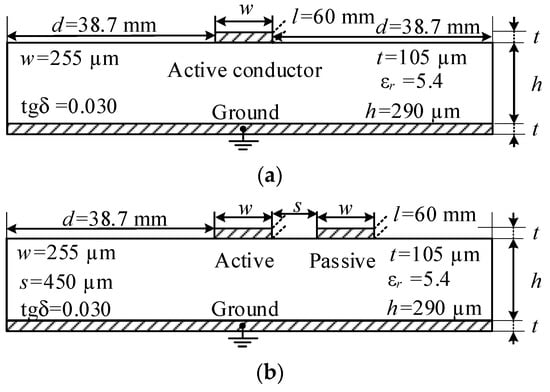
Figure 120.
The cross-sectional parameters of the structures without (
a
) and with (
b
) MR.
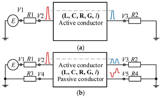
Figure 21. The structures without (a) and with (b) MR: equivalent schematic diagrams where R = 50 Ω and E is a harmonic electromotive source with an amplitude of 1 V.
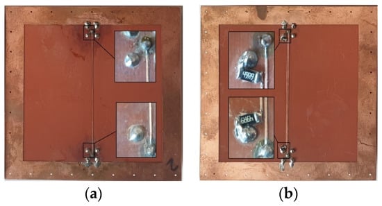
Figure 322.
The PCB prototypes without (
a
) and with single (
b
) MR.
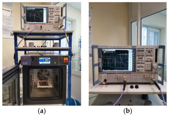
Figure 423.
The climate heat-cold chamber (
a
) and the vector network analyzer (
b
).
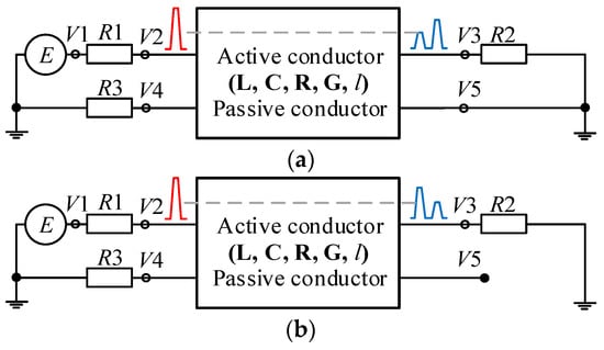
Figure 524. The structures with single MR after SC (a) and OC (b) failures: equivalent schematic diagrams where R = 50 Ω and E is a harmonic source with an amplitude of 1 V.
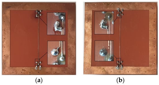
Figure 625.
The PCB prototypes with MR after SC (
a
) and OC (
b
) failures.
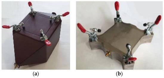
Figure 726.
The classical (
a
) and miniature (
b
) TEM-cells.
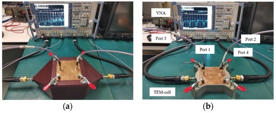
Figure 827. The connection of VNA ports to the input and output of the classical (a) and miniature (b) TEM-cell CC (Ports 3 and 4), and to the PCBs (Ports 1 and 2).