The use of fuel cells in DC microgrids has been receiving a lot of attention from researchers and industry since both technologies can deliver clean energy with little to no environmental impact. To effectively integrate fuel cells in DC microgrids, a power converter that can equate the fuel cell’s voltage with the DC microgrid’s reference voltage is required. Based on the typical output voltages of fuel cells, buck-boost topologies are commonly used in this type of application. ThisA work compiles, compares and describes differentvariety of DC-DC buck-boost topologies that have been introduced, showing distinctive merits and drawbacks, are available in the literature over the past few years.
- fuel cell
- DC microgrids
- buck/boost converters
- Ćuk-based converters
- quadratic converters
- fault-tolerant converters
- efficiency
1. Introduction
2. Coupling Behavior between FCs and DC-DC Converters
The coupling behaviour between FCs and DC-DC converters was first studied in [16]. In this study, a model aiming at understanding the requirements for the connection between FCs and power converters was developed [16]. It was concluded that, for high frequencies, the electric equivalent model of the FC can be reduced to the internal resistance. Furthermore, the presence of a high capacity at the interface between the electrode and electrolyte, referred to as a double layer capacitor, or CDL, means that the current harmonics are easily filtered by the FC [16]. A scheme of the FC is shown in Figure 2. The study also provided some conclusions on the coupling behaviour between FCs and buck-boost converters. The results showed that the converter input voltage ripple for the boost converter is five times lower than that of the buck converter [16]. Despite the relevant conclusions obtained in [16], the long-term effect of the high current ripple on the CDL was not considered.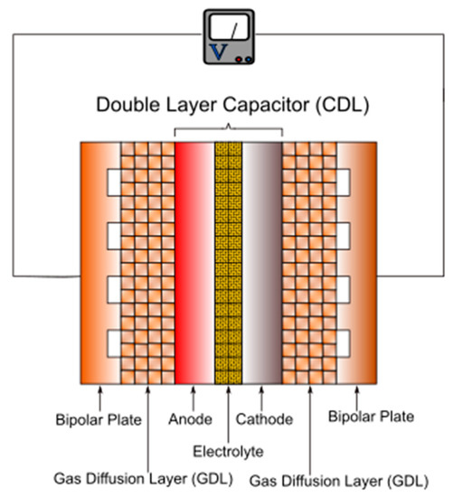
3. Buck-Boost Topologies
The previous section presented the coupling behaviour between the three most basic DC-DC power converter topologies. As mentioned, the buck-boost topology introduces large oscillations in FC voltage and current that ultimately lead to fuel waste and decrease efficiency. The conventional buck-boost topology is shown in Figure 3a. It has a very reduced number of components and the output voltage polarity opposes the input one [20,21]. To solve the oscillation problem, a plethora of different buck-boost topologies have been proposed over the past few years. Although these topologies can be categorised according to the numbers of power switches, some authors also categorise buck-boost converters as current- or voltage-source converters [13].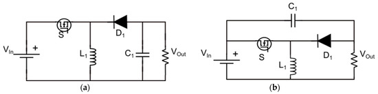
3.1. Ćuk-Based Converters
The EĆuropean Union has set an ambitious goal for 2050: aiming to become a carbon-neutral society, withk converter, represented in Figure 4a, more competitive economy, whose growth is fully dissociated from resource use. Working towards this goal will inevitably change the EU’s societal paradigm into a fairer and more prosperous one [1]. The short-is another common buck-boost converter. This converter is used in many differenterm goal, set for 2030, is to reduce greenhouse gas emissions (GGE) by at least 55% [1]. Produciapplications, rang einergy throughg from renewable sources is envisioned as a promising wayenergies [22,23] to accomplish this goal. Therefore, support for the adoption ofower factor correction [24]. rThenewable energy technologies is expected to grow exponentially main merits of this converter are its low output [1].
Cvonneclting different renewable energy sources on a single AC grid poses many technical and functional challenges siage ripple and non-pulsating input and output currents [25]. Ince each source has a different voltage profile and requires different energy conversion stagescontrast, the inverted polarity on the output side is the main drawback. In addition, and [2]. A possibldue way to solve this issue is to use a microgrid, which is smaller, more efficient, and more reliable than a the presence of just one power switch, this converter shows high component stresses and low conventional AC gridrsion efficiency [2][26]. This grid coperates at a lower DC voltage level than the traditional AC grid and can easily incorporate various renewable sources, such as photovoltaic (PV) systems, wind turbines or fuel cells (FCs), as well as different energy storage systems, such as batteries, supercapacitors, flywheels and hydrogen storage systemsnverter contains two inductors and two capacitors. This means that it is a high-order power converter with [2]. Furthrermore, DC microgrids can either work independently of the main grid, in is-landed mode or connected to it, in grid-connected mode [2]e zeros in the right half plane (RHP), thus making its control quite complex.
Nowadays, DC micrTogrid applications mostly rely on PV technologies. Nevertheless, the use of FCs in micr solve this problem, authors in [27] ogrbtaids has been studied and researched thoroughly by industry and scholars alikened its fourth-order transfer function, using state space analysis [2].(SSA), Uanlike other renewable sources, FCs do not depend on external factors such as the wind or the sun. FCs also have a substantiallyd conducted an order reduction using higherPadé appower/volume ratio thanroximation [27]. otTher renewable sourcesy were able to reduce [3].
Tthe soriginafe and efficient connection of the voltage characteristic of the FCl two pairs of complex poles in the left half plane (LHP) and the reference voltage of its application requires the integration of power electronic converters between the FC and the DC microgrid. Different nominal voltages have been provided by FC manufacturers over the past years, with manufacturers aiming to offer even higherthree zeros in the RHP, to just one RHP zero and one pair of complex poles, transforming it into a second-order system [27]. vToltage levels a access the technology progresseseffectiveness [4]. Thereofore, when designing a power converter for FC applications in DC microgrids, buck-boost topologies, which can provide lower, equal or higher output voltage levels, are necessarythe model order reduction, a step response was performed on both transfer [4]. Bfunck-boost topologies enable three distinctive operation modes in a single converter: the buck-mode,tions. The results showed a good approximation between the two models [27]. whichTo happens when the input voltage is higher thaobtain enhanced control capability on the output voltage; the boost-mode, also known as the set-up mode, which occurs when the output voltage is higher than the input voltage; and the third mode, which happens w, a simple compensator was designed using the second-order transfer function [27].
Then the input voltage is very similar to the output voltage, hence referred to as the buck-boost mode. Over the years, FCs were mostly employed on electric vehicles. As a result, there is a variety of work concerning FC systems applied to e-mobility solutions [5],[6],[7],[8],[9],[10]. Oproblem of inverse polarity at the converter output can be overcome by means of an isolation the other hand, there is a lack of researcansformer [28]. This concerning buck-boost topologies for FC applications in DC microgrids.
Despiteverter is referred to as all of then benefits associated with adopting power isolated Ćuk converters, their switching nature introduces ripple, which might affect the FC performance, and thus, the system’s efficiency [11]. The and has the same advantages as its predecessor. In addition, it also provides electrippcale is mostly noted o isolation between the current, generating unwanted effects, such as fuelinput and output, as shown in wasteFigure 4b. aInd [28], thigher losses, low reactant concentration, accelerated electrode ageing and decreased FC durabilitye isolated converter was used to [4],[11].
2. Coupling Behavior between FCs and DC-DC Converters
The interfaction between buck, boost, and buck-boost converters and FCs were analysed in [11]e a pulsed load with a FC. TheIn root causes of oscillations in the current and voltage of the FCs and possible mitigation solutions are presented [11]. Fthis application, the load operates at a constant voltage orf the boost converter, the analysis was performed under three different scenarios. All scenarios started with the same load resistance. The first scenario kept the load resistance constant; for scenario number two, a load step was8 V, while pulsed current is drawn to the load. The experimental results were performed, with the resistance being reduced; as for scenario number three, a load step was introduced, with the resistance being increased under an increasing pulsed current and different loads [11][28]. BotTh scenarios one and twoe results showed no significant impact on the oscillation of that the FC output. In turn, and due was successfully connected to the low FC outputpulsed current for scenario three, the same voltage oscillation can no longer be neglected [11]. Thereload. Despite the interesting benefore, for low current densities on the FC, the boosts of the isolated Ćuk converter negatively affects the voltage oscillation [11], some drawbacks should be considered. ThOne occurrence of these phenomena can be reduced if a capacitor isdrawback is the presence of a transformer, which introduced in between the FC and the boost converter or if the converter switching frequency is increased. This latter option increases the switching losses on the converter [11]. Ts undesired parasitic losses and limits the available duty cycle range, in both modes of operation evaluate the buck converter, two scenarios were considered. For the first scenario, the FC was operated close to the maximum point with a constant duty cycle (buck or boost). The ratio between the output voltage and input voltage is equal to onethe inverse [11]. Inof the transecond scenario, a load step was introduced such that the FC could operate at a lowerformer ratio times the ratio between the power ratingswitch in [11]. Tthe reON sults showed that fortate over the OFF state [29]. scHenario one, no oscillation in the FCce, to have equal voltage was observed since the converter switch was always on, while for scenario two, large oscillations ingain for both buck and boost modes, the ideal transformer turns ratio must be equal to one.
|
|
|
|
(a) |
(b) |
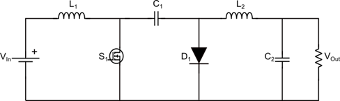
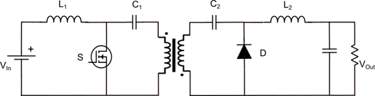
Figure 4. Ćuk bcoth FC current andnverter (a). vIsoltage were observed [18]ated Ćuk converter (b).11 Suc
The large oscilelectrical isolations increase fuel consumption and FC temperature. These consequences were not considered in this study. The oscil between the input and output, provided by the isolations can be mitigated if transformer, provides the converter switching frequency is increased or if the FC CDL is increased [11]with extra security in case of a fault. ThLis latter technique is implemented by introducing a large capacitor in between the FC and the ke the isolated Ćuk converter, push-pull converters [11].
The coupliang behaviour between the FC and the buck also be used as buck-boost converter can be used to estimate the FC parameters, such as the exchange current and the transfer coefficient, by measuring the average inductor current and the amplitude of the FC voltage oscillation. These variables are then considered as inputs fors. This converter is based on the forward converter; however, it possesses an extra power switch and a different connection to the intermedium transformer, as depicted in Figure 5a. mathematical model, derived inThe additional power switch [11]. Finally,ows the coupling behaviour between the FC and the buck-boost converter was analysed. The results showed that, due to the presence of a switch in series with the FC output, the buck-boost converter also introduces large oscillations in the FC variableurrent to flow continuously through the primary winding of the transformer, as long as the power switches have opposing switching signals [11][30].
The lcontiterature shows that the nuous flowing of current ripple can have a negative effect on the efficiency and overall lifetimethrough the primary input of the FC [12]. Thetreansfore, it is necessary to choose a power converter topology capable of eliminating such negative effects by limiting the converter input current ripplemer increases its efficiency and, consequently, the cost and the number of components, while preserving highoverall converter efficiency. The next section describes different buck-boost topologies that are suitable for FC applications in DC microgrids, with a focus oWhen S1 is ON, a positive voltage is induced in the main merits and demerits of each one.
3. Buck-Boost Topologies
Theprimary and secondary windings of the ptrevious section presented the coupling behaviour between the three most basic DC-DC power converter topologies. As mentioned, the buck-boost topology introduces large oscillations in FC ansformer. Hence, diode D1 is conducting, and the inductor L1 starts to store energy in the form of a magnetic field. In turn, when S2 is ON, a negative voltage and current that ultimately lead to fuel waste and decrease efficiency. It has a very reduced number of components, and the output voltage polarity opposes the input one [13]is induced in the primary and secondary windings of the transformer. Therefore,[14]. ToD2 solve the oscillation problem, a plethora of different buck-boost topologies have been proposed over the past few years. Although these topologies can be categorised according to the number ofis conducting, while inductor L2 releases its energy. Ideally, there is no delay between the switching signals of the two power switches, some authors also categorise buck-boost converters as current- or voltage-source converters.
A continuous input-current buck-boost (CIbB) DC-DC converter for proton-exchange membrane (PEM) FC applications, which is based on the conventional single-switch buck-boost converter, was introduced in [4]. The converter possesses a capacitor connected between the positive terminal of the input voltage source and the negative terminal of the load [4].3.1. Ćuk-Based Converters
Th; nevertheless, due to the microse Ćuk converter, represented in Figure 2a, isd delay in another common buck-boost converter. This converter is used in many different applications, ranging from renewable energies rise time of physical power switches, for example in [15]MOSFET,[16] tosuch power factor correctioa condition can [17]happen. The mnegain meritstive impact of this converter are its low output voltage ripple and non-pulsatingdition is a discontinuity of both input and output currents [18]. InTo contrast, the inverted polarityavoid this problem, authors in [31] ochan the output side is the main drawback. In addition, and due to the presence of just one power switch, this converter shows high component stresses and low conversion efficiencyged the inductor location to the input primary input of the transformer, hence limiting the abrupt change of the input current. The authors also highlighted [19].
Tthe improblem of inverse polarity at tortance of overlapping the converter output can be overcome by means of an isolation transformduction moments of both power [20]. Thswis tconverter is referred to as an isolated Ćuk converter and has the same advantages as its predecesshes, with the aim of safely connecting the inductor. In addition, it also provides electrical isolation between the input and this configuration, the output, as shown in Figure 2b. Des capacite the interesting benefits of the isolated Ćuk converter, some drawbacks should be considered. One drawback is the presence of a transformer, which introduces undesired parasitic losses and limits the available duty cycle range, in both modes of operation (buck or boost). The ratio between the output voltage and the input voltage is equal to the inverseor needs to have a reasonably significant capacity. This is because when the switching signals of S1 and S2 are overlapped, no electric and magnetic field is induced in the secondary winding of the transformer ratio times the ratio betweedue to cancelled flux in the power switch inrimary winding [31]. tThe ON state over the OFF staterefore, the load must [21]. Hbence, to have equal voltage gain for emporarily supplied only by the output capacitor [31]. Figure 5both buck and boost modes, the ideal transformer turns ratio must be equal to oneillustrates the proposed converter.
|
|
|
|
(a) |
(b) |
|
|
|
|
(a) |
(b) |
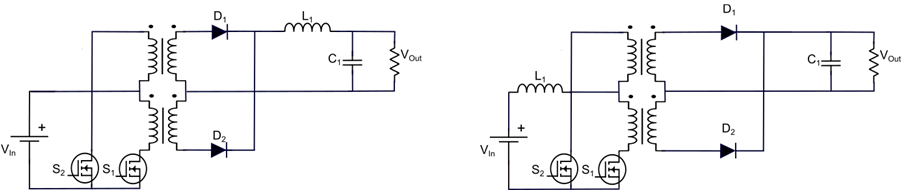
Figure 25. ĆBuk ck-boost push-pull converter (a). IsolaCurrented Ćuk c-fed push-pull DC-DC Converter (b).
TWhe electrical isolation between the input and output, provided by the isolation transformer, provides then compared to the isolated Ćuk converter, the buck-boost push-pull converter with extra security in case of a fault. Like the isolated Ćuk converter,shows worse continuity at the input current. The control approach for the push-pull converters can also be used as buck-boost converters. This converter is based on the forward converter; however, it possesses an extra power switch and a different connection to the intermedium transformer. The additional is also more complex because the time delay of the power switches must be considered if a non-overlapping strategy is used or if both duty-cycles are greater than 0.5. For the isolated Ćuk, the control approach is much simpler since there is only one power switch allows the current to flow. Another distinguishing factor between the two converters is the continuously through the primary windingity of the output current. The output current of the transformer, as long as the power switches have opposing switching signals [22]. Thisolated Ćuk has significantly lower ripple contienuous flowing of current throught when compared to that of the primary input of the transformer increases its efficiency and, consequently, the overallush-pull. Therefore, a more robust output current control can be achieved on the isolated Ćuk converter efficiency.
Another Ćuk-based converter was introduced in [[323]]. This converter not only exhibits similarities with the Ćuk converter, since both have a single power switch, but also possesses similarities with the SEPIC converter, because of the positive voltage output [[323]]. Both Ćuk and SEPIC converters are limited to a maximum theoretical voltage gain of 10—in practice, such gain is lower due to the converter conduction and switching losses [32].23 To solve this issue, while increasing the overall converter efficiency, authors in [[323].] excluded the hybrid switched-capacitor structure, and added extra passive components, such as inductors, diodes and capacitors. The improved version of the converter, irepresented in Figure 6a, is composed of a single power switch, four diodes, three inductors and six capacitors (SSBb) [[323]]. This modification increased the voltage gain by three times and, consequently, the boost range [[32]. In the paper, the converter was tested with a 660 W PV system and a 550 W FC operated under different hydrogen supply pressures [3]2]. The efficiency, defined as the maximum efficiency obtained for a load current of 1 A and the minimum efficiency obtained for a load current of 12 A, was reported to range between 91% to 98%. The authors also suggested a control algorithm based on the theoretical calculation of the duty cycle, which is determined by the desired output voltage and measured input voltage. This algorithm may have difficulties operating under variable loads since there is no feedback from the output voltage. The acquisition of the input voltage may also present a challenge to the effective implementation of the control strategy because it is necessary to suppress all the noise and ripple, which would require a more complex input filter. This drawback could be mitigated if feedback from the output voltage was introduced. Apart from the sensitivity of the controller to perturbations, the main disadvantage of this converter is the pulsating output current, which implies higher capacitance at the converter output.
OAnother suitable solution for FC applications was introduced in [24][33]. The converter (CBSS), ipresented in Figure 6b, is derived from the Ćuk converter, so it inherits its advantages. In addition, it reduces the inrush currents and the stress imposed on diodes, switches, and capacitors [24][33]. This converter also has some features of the KY converter, namely the reduced voltage stress on the components. During the OFF state of the power switch, two more modes are added, so the stress on the components is reduced [24][33]. The voltage gain is two times the one of the Ćuk converter, so there is an increase in the boost range [24][33]. Despite the considerable advantages of this converter, there are some drawbacks to consider. One of them is the reverse polarity of the output voltage. This feature, inherited from the Ćuk converter, imposes higher voltages across the intermediate capacitors, which increases the risk of short-circuit failure. Therefore, particular attention should be paid to polarity-inverting topologies with regards to capacitor state of health. The adoption of condition monitoring strategies aimed at capacitors could be useful in preventing the short-circuit problem. The high number of passive elements, which potentially increases the parasitic losses, can be considered as another drawback of the converter [33]. Some suggestions for future work include studying the inner dynamics of the converter and applying different control strategies [33].
|
|
|
|
(a) |
(b) |
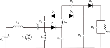
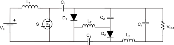
Figure 6. Single-switch boost-buck converter (SSBb) (a). Ćuk-based single-switch buck-boost converter (CBSS) (b).
As already explained, most converter suitas presented so far have at least one zero in the RHP. This is explained by the fact that such converters were derived from the boost converter, which consists of a non-minimum phase system [34]. The literature introduces different solutions to deal with the negative effect of zeros in the RHP. In [35], the proposed technique is based on the inductor current being artificialle for Fy imposed on the voltage feedback network, thus obtaining the transfer function corresponding to the OFF state of the power converter. Another technique was introduced in [36], where a two-inductor boost converter superimposed with a buck converter solved the RHP problem. For both techniques, complex drivers are required.
A converter suitable for FC applications in DC microgrids was first introduced in [26][37]. This converter (TSBb), presented in [25][34], suppresses the effect of the RHP zero by using magnetic coupling inductors and damping networks. The authors were able to mitigate the effect of the RHP through the use of magnetic coupling between the input and output inductors. They were also able to increase the inner dynamics using the damping network, constituted by a capacitor in series with a resistor, which functions as a low-frequency snubber that increases the bandwidth of the proposed converter [26][37]. The configuration of the converter is based on a cascaded connection between the boost and buck converter, producing a double-switch converter with low components stress and high efficiency, as depicted in Figure 37a [37]. Both conversion stages (buck and boost) possess dedicated inductors that provide non-pulsating currents both in the input and output, low noise level, and some control versability, since it is possible to independently control both the input and output currents [37]. The authors also extracted the transfer function of the converter, concluding that it is a second-order system similar to the buck’s control-to-output transfer function. Therefore, the design of the controller is simplified and it is possible to use well-established control methods [37].
|
|
|
|
(a) |
(b) |
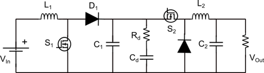

Figure 3. The operation principle is quite simple. For buck mode, the powo-er switch of the buck module is switch boost-buck coning, while the boost power switch is kept open. For the boost mode, the buck power switch is kept in the ON state, while the boost module is switching [37]. This converter has already been used in different microgrid applications integrating hybrid energy generation systems. In [38], a FC system hybridised with an auxiliary storage device (ASD) was implemented using the proposed converter. TSBhe converter’s control versatility allowed for rapid changes between current control and voltage control depending on the energy level demanded from the microgrid and the ASD [38]. A similar work was reported in [39]. Here, both the FC and ASD act as energy sources, so the microgrid’s voltage does not depend solemnly on the FC [39]. It is necessary to implement more than one converter to properly transfer energy from both input sources to the microgrid [39]. Lastly, a comparative study evaluated different topologies of hybrid systems using FCs and ASDs [40]. The topologies were denominated according to the position of the FC and the ASD: serial hybrid (SH) ; parallel hybrid (aPH) and serial-parallel hybrid (SPH). NTo compare the three topologies, tests with constant and pulsed loads were perfovel high gain sinrmed. The results showed that the SPH topology is more efficient than the other topologies, so it is the topology recommended for applications whose load profile is unknown [40]. Despite the mentioned advantages, the converter presents a proble-switm working in buck-boost mode. This problem is due to the challenging transition between the two operation modes (buck and boost), and it is referred to as the dead zone transition [41]. As described, th DC-DCere are only two operation modes, which can be a disadvantage when the input voltage is very similar to the output voltage. Thus, it is important to guarantee that the converter can either operate in buck, boost or buck-boost conmode. To eliminate this challenge, some authors have presented different solutions to mitigate the dead zone. The solutions presented in [42,43] are based on the overlap beter with ween buck and boost modes. This method increases the switching losses and only partially solves the discontinuoity between the two modes [41]. A more appropriate method was introduced in [44]. In this method, the overlappinput and output pog concept is preserved, while a maximum threshold is established for the duty cycle applied in buck mode. Later, it was found that the proposed method caused a reduction in the efficiency in buck-boost mode. To solve this problem, the authors that proposed the converter in [37] developed a mitigation algorithm that overlapped the buck and boost modes, whiler clamping the limits of the duty cycle with a hysteresis window [41]. (NISBWith this method, it was possible to obtain the three modes of operation and to achieve a smooth transition between buck and b) (b)oost [41].
A more recent Ćuk-based topology (NISBb) was presented in [27][45]. This converter uses only a single power switch with lower stress, four diodes, four capacitors and three inductors. Unlike its predecessor, this converter has the same output polarity as the input, and the disposition of the capacitors, as illustrated in Figure 7b, provides a significant higher voly higher voltage tage gain when compared to the Ćuk converter. When the power switch is ON the input source provides energy to the inductor L1, while the load is being fed by the capacitors C1, C2 and C3. For the OFF state, the energy stored in the magnetic field of L1 is released to charge the capacitor C1 [45]. At the same time, the energy stored in inductors L2 ain nd L3 is used to charge capacitors C2 and C3 and provide energy to the load [45]. Despite the low stress on then compared to the Ć power converter, the gain of the converter does not provide similar ranges for buck and boost mode, which limits its application. Moreover, additional experiments are needed to access the converter’s efficiency.
|
|
|
|
(a) |
(b) |


Figure 7. Two-switch boost-buck converter (TSBb) (a). Novel high gain single-switch DC-DC buck-boost converter with continuous input and output power (NISBb) (b).
All in all, Ćuk-based converters are very suitable for FC applications in DC microgrids. Most of the presented converters possess both continuous input and output currents, which helps reduce the negative impact of the current ripple in the FC and allows for enhanced and more accurate current control. The continuity of the input current is possible due to the presence of an inductor in series with the input, meaning that at least one zero will be present in the RHP. The negative effect of such an inductor can be neglected, or at the bare minimum reduced, if coupled inductors are used. The adoption of a more adaptive approach, based on predictive control could also help. In addition, most Ćuk-based converters only possess one switch, which means that the duty cycle range will be half for the buck mode and half for the boost mode. The third mode, buck-boost, is theoretically obtained when the duty cycle is equal to 0.5. For topologies which possess more than one power switch, such as the TSBb, the duty cycle range is extended.
3.2. Quadratic Converters
The voltage gain of any DC-DC converter is an important factor when choosing the correct topology for a specific application. For applications whose input and output voltage levels are significantly different, the use of isolation transformers, which provide safe integration between input and output, is an interesting solution. Another possible solution consists of the use of quadratic converters. These converters have a quadratic gain, which means that they are suitable for applications whose input and output voltage levels are very different [28][46,[29]47]. Several high-gain boost DC-DC converters have been presented in the literature. These converters provide a wide input voltage range and have therefore become crucial for FC applications in electrical vehicles [30],[31],[32][48 49 50]. In [28][46], a quadratic buck-boost converter with positive polarity at the output voltage and continuous input current (QBBPO) is presented. Both power switches of the converter have the same switching signal, whose duty cycle is the nominal duty cycle of the converter [28][46]. This converter resembles a cascaded configuration of two traditional single-switch buck-boost converters. To solve the input current continuity problem that is characteristic of the original converter, a group of two capacitors is inserted in parallel in between the input and output. The effective converter operation is strongly dependent on the correct behaviour of the two capacitors that filter the input and output currents. The converter is illustrated in Figure 48a.
The converter proposed in [29][47] is a combination ofbetween three basic converters: boost, buck-boost and buck converters (SSQBB). Along with the quadratic gain, this converter also has continuous currents at both input and output and possesses a single power switch. Thus, following the cascade sequence, the output voltage of the boost stage is the input of the buck-boost stage, and the output voltage of the buck-boost stage is the input voltage of the buck stage, as shown in Figure 48b. The continuity of the currents is achieved thanks to the inductors from the original circuits of the buck and boost converters. Theoretical analysis showed that the efficiency of the converter increases with the duty cycle, so the converter is more efficient when working on boost mode [47]. The experimental results showed that the higher efficiency was achieved when the voltage gain was higher, resulting in enhanced efficiency for the boost mode. The experimental results also suggested that the dynamics of the converter are satisfied. However, a more thorough analysis of the transfer function aimed at not only understanding the inner dynamics, but also optimising the control strategy, is required. Even though the quadratic gain and the non-pulsating currents are significant advantages of the converter, its practical implementation may be limited by drawbacks such as the reverse polarization of the output voltage and the limited efficiency in buck mode. Other quadratic gain buck-boost topologies were introduced in [51,52]. Despite their reduced number of components when compared to the converter presented in [47], they have pulsating currents at the input, which are unsuitable for FC applications.
|
|
|
|
(a) |
(b) |
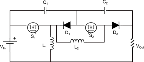
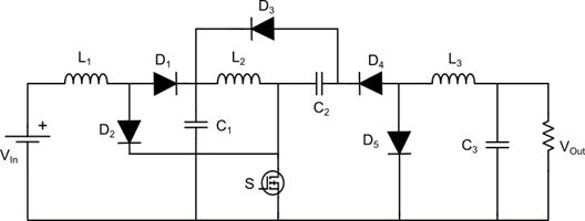
Figure 48. Quadratic buck-boost converter with positive output voltage and continuous input currents (QBBPO) (a). Single-switch quadratic buck-boost with both input and output current continuous converter (SSQBB) (b).
Both converters possess the same voltage gain; however, the total number of components is quite different. The QBBPO obtains quadratic gain characteristics without the use of transformers or coupled inductors; rather, it employs the same duty cycle on the power switches. On the contrary, the SSQBB converter uses just one power switch and two storage elements that transfer and store the energy to reach the quadratic voltage gain.
To solve the problem of pulsating currents, a semi-quadratic converter with positive voltage output (SQBuBoC) was introduced in [[533].].The converter is shown in Figure 9a. It consists of two power switches that are operated simultaneously (as is the converter in [28][46]), two inductors, two diodes and two capacitors. It has a continuous input current, a wide output voltage range and non-inverting voltage polarity [[533]]. The low voltage stress across the power switches also improves the converter’s efficiency [53]. When compared with similar converter structures, [the efficiency of this converter is higher, thanks to the lower number of components and low voltage stress. The analysis of the transfer function suggests the presence of one zero in the RHP and two in the LHP, as well as two pairs of conjugate poles. The zeros of the system are very suitable to extreme displacement under load variation, meaning that the damping ratio and the settling time will increase for higher output loads [53]. When both output voltage and load are kept constant and there is a change in the input voltage, the effects of the RHP are reduced when the duty cycle is decreasing because the zero is placed far from the origin. On the other hand, when the LHP zeros are closer to the origin, this introduces some instability into the system. To optimize the converter performance, it should operate within the high power range, which implies the adoption of a higher duty cycle [53]. Despite the positive features of the presented converter, some considerations should be made regarding the output current.
For applications that require low output current ripple, a capacitor with high capacitance is required, which may lose its filtering effect if placed in parallel with a battery. A similar converter (NOBB), represented in Figure 9b, was introduced in [3[54]. Both power switches have the same duty cycle, so a semi-quadratic gain is obtained [3[54]. The input current ripple of this converter is slightly larger in comparison to other semi-quadratic converters because the inductor is not directly placed in series with the input voltage source. Changing the position of the input inductor would improve the filtering capacity of the input current. As expected, the experimental results showed a higher efficiency for the operation in step-up mode. Still, the peak efficiency (around 83%) is low when compared to the other topologies presented previously.
have lower values than that of other converters. Regarding the quadratic converters, all of them have the same number of components, except for the SSQBB. They are mostly used in applications where the voltage levels, an inductor, a diode and a power switch. Meanwhile, the interleaved version allows for low input current ripple, which reduces the damage to the FC. To control the input current of the converter, the authors used a current control loop that calculates the duty cycle according to the error between the input and output are verycurrent and the reference signal. To ensure a low input ripple, the different. The reported efficiency varies between 60% and 95% for power outputs lower than 100 W. As expected, the fault-tolerant topologies have a higher number of components. This is due to the fault-tolerant strategy itself which requires that a finite number of PWM signals applied to each converter arm were shifted 90° in sequence with the 0° phase acting as the master control and the following 90°, 180° and 270° as the slave controls. The input current signal was sampled at every turn-on point of the master control signal. The experimental results showed a maximum conversion efficiency of 93% when the converter components be in paradopts a constant current, voltage and power control.
 |
Talblel with each other, hence requiring a higher 1 presents a compilation of the main characteristics of each converter such as the number of components. Moreove, current profile, gain and reported efficiency
Table 1. Compar,ison between these t state-of-the-art converter topologies present a higher efficisuitable for FC applications.
From the table, it is noted that the total number of components is generally lower for the Ćuk-based converters. This is because these converters only rely on a single switch, larger capacitors and larger inductors. Another notable aspect of the Ćuk-based converters is the relation between the total number of components and the output voltage polarity. Converters such as SSBb, TSBb and NISBb possess a positive output polarity, which means that they have a higher number of components when compared to converters such as CIbB and Ćuk. This translates into a higher efficiency because the stress on the power switch and diodes are lower. In addition, the required inductors and capacitors have lower values than that of other converters. Regarding the quadratic converters, all of them have the same number of components, except for the SSQBB. They are mostly used in applications where the voltage level between input and output are very different. The reported efficiency varies between 60% and 95% for power outputs lower than 100 W. As expected, the fault-tolerant topologies have a higher number of components. This is due to fault-tolerant strategy itself which requires that a finite number of the converter components be in parallel with each other, hence requiring a higher number of components. Moreover, these topologies present a higher efficiency, with values ranging from 91%-95% for power outputs close to 40 kW.
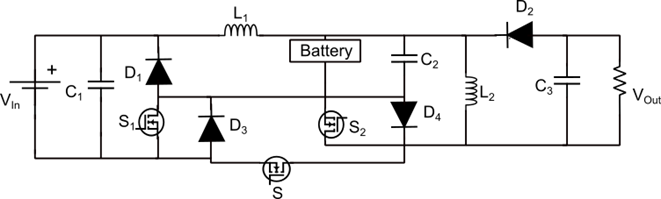
The voltage gain of the Ćuk-based converters, quadratic converters and fault tolerant converters can be easily compared using Figure 12a–c, respectively.
In Figure 12a, it is important to notice that for the inverting topologies, the modulus of the voltage gain was considered. It is also clear that topologies such as CIbB, Ćuk and Isolated Ćuk have the same voltage gain. The TSBb converter shows a lower voltage gain but has a higher range for buck and boost mode than the other converters. Figure 12b shows that quadratic converters have higher voltage gains, albeit at the expense of lower buck ranges, when compared to other converters. Finally, from Figure 12c, it is concluded that the 4PIBb converter has the same voltage gain as most of the Ćuk-based converters, while the other two topologies present a behaviour similar to that of the TSBb converter.
|
|
|
|
(a) |
(b) |
|
|
|
|
(a) |
(b) |
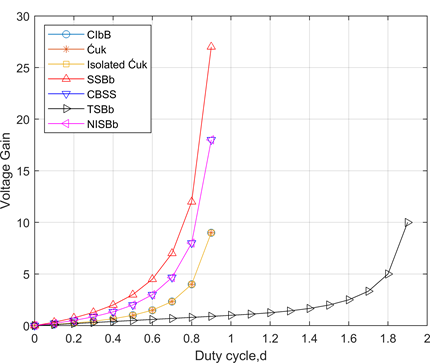
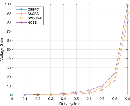
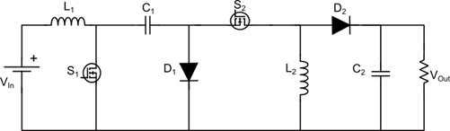
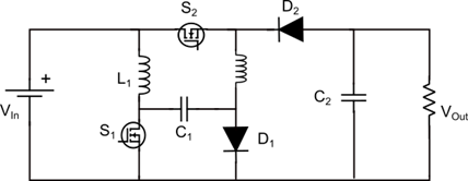
Figure 9. Transformer-less semi-quadratic buck-boost converter (SQBuBoC) (a). Semi-quadratic negative output buck-boost converter (NOBB) (b).
3.3. Fault-Tolerant DC-DC Converters
To assess the reliability of power electronics converters, a previous study reported on the results of a questionnaire survey which was conducted to determine the main elements of a power converter that are prone to failure in industrial applications [3[55]. Different semiconductor manufacturers from the aerospace, automation sector and utility power sectors were asked to answer the questionnaire. Questions ranged from power device operating conditions to failure counteraction and costs. The results showed that, within all elements of a power converter, semiconductors, such as IGBTs and MOSFETS, represented 31% of all failures. In contrast, capacitors represented less than 20% of failures, while gate drivers corresponded to 15% of failures [3[55]. This study clearly shows the importance of semiconductor failures in power converter functions.
Although most studies emphasise aspects like reduced components stress, control, and efficiency optimisation, very few fault mitigation strategies have been presented so far. Although it has not been thoroughly addressed, support for the adoption of the interleaving technique to build a fault-tolerant converter structure has been gaining in strength. The interleaving technique is based on connecting multiple layers of the converter in parallel, while shifting the phase by the inverse number of paralleled arms in the converter [4][8]. This technique helps to reduce the ripple on the input current, and most importantly, assigns fault tolerance to the converter, thus offering extra reliability.
Profiting from the benefits of the interleaving technique, a novel structure of the converter is proposed in [4].[8] was derived. This new structure has two arms, so it has twice the components of the original one. Since the current is shifted in each arm, the total current ripple is cancelled, which means that smaller inductors can be used to obtain the desired current ripple [4][8]. Another topology with a fault tolerance mechanism (FTbbB) is presented in [3[56]. The authors proposed a fault-tolerant two-stage buck/buck-boost converter with tolerance against open-circuit switch failure that uses redundancy acquired through a synchronous switch for the power switches. The redundant circuit is composed of a single switch and two diodes, hence keeping the number of redundant switches to a bare minimum [3[56]. The experimental results showed that the control algorithm was able to quickly adapt from the healthy to the faulty state of operation [56]. The converter is represented in Figure 510a.
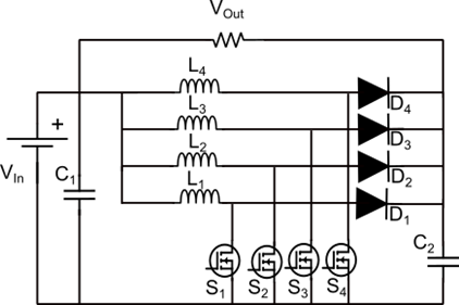
MoThe intere recently, a buck-boost topology (4PIBb) was presented ileaved technique can be used to reduce the current ripple on [37]the FC. TMoreover, this topology uses a four-arm echnique can also improve the efficiency and reliability of the converter. For a non-interleaved boost converter with changed load connection. In practice, this means that the l, it is common to increase the switching frequency to reduce component size and the current ripple. However, high switching frequency can cause an increase in the switching losses [57]. To ad is connected between the cathode of the output diode and the void this, one can use the interleaving technique to divide the input power by the multiple arms of the converter [57]. This technput capacitor, resulting in an iique has already been proven to help increase both the efficiency and reliability of the convertedr [58,59]. One coutput voltage. This configuration,nverter that also uses this technique (ISUSD) was proposed in [57]. rThepresent proposed technology, illustrated in Figure 510b, allcows for both continuous input and output currents and enables operation in both buck and bonsists of a conventional buck module and a floating boost modes, which the traditional boostule, where the input terminal of the converter cannot provide.
 |
 |
| (a) | (b) |
Figure 5. Fis connected in parallel, while the analogous oult-tolerant buck/buck-boost convertetput terminal is connected in series [57]. Prior to (FTbbB) (a).that, each Fmourdule possesses a two-phase interleaved buck-boost converter (4PIBb) (b).
Table 1 pstructure in order to resducents a compilation of the main charact the ripple in the FC current [57]. The woristics of eachking principle of the converter such as the number of components, current profile, gain and reported efficiency.
Table 1. Cis quite simple: the buck mode is obtained by switching the power switch of that module and keeping the boost’s switch omparison between the state-of-the-art converter topologies sen, while for the boost mode, the buck power switch is kept closed and the boost’s switch is switching [57]. Even though the itable for FC applications.
Fromnterleaving technique helped reduce the ripple effect on the FC table, it is notcurrent, especially for buck mode, the results showed that the total number of components is generally lowerinput ripple was not satisfactory. This issue can be addressed if additional arms are introduced for the Ćuk-based converters. This is because thesbuck module or if the duty cycle is kept below the inverse of the number of arms. To control the input current of the converters only rely on a single switch, larger capacitors and larger inductors. Another notable aspect of the Ćuk-based converters is the rela, a proportional integral (PI) controller was designed and an average current method was deployed to ensure a smooth transition between the total number of componwo modes of operation [57].
| |
|
© |
|
|
|
|
|
(a) |
(b) |
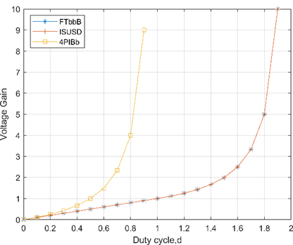

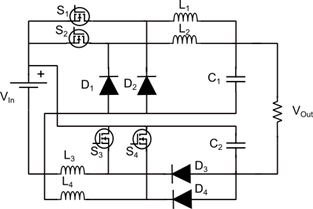
Figure 10. Fault-tolerants and buck/buck-boost converter (FTbbB) (a). Inthe output voltage polarity. Cerleaved step-up/step-down converters (ISUSD) (b).
More surech as SSBb, TSBb and NISBbently, a buck-boost topology (4PIBb) was presented in [60]. This topossess a positive output polarity, whichlogy uses a four-arm interleaved boost converter with changed load connection. In practice, this means that they have a higher number of components when compared to converters load is connected in between the cathode of the output diode and the input capacitor, resulting in an inverted output voltage. This configuration, represented in Figure 11, allowsuc for both as CIbB and Ćuk. This translates into a higher efficiency because the stress on the power switch and diodes is lower. In addition, the required inductors andcontinuous input and output currents and enables operation in both buck and boost modes, which the traditional boost converter cannot provide. Furthermore, this converter has a relatively low number of components, since the non-interleaved version only requires two capacitors
Figure 12. Cuk-based concy, with values rangingverters voltage gain (a). fQuadrom 91%-95% for poweratic converters voltage gain (b). oFautputs close to 40 kWlt-tolerant converters volage gain (c).
For future work, more robust control approaches, such as the Model Predictive Control (MPC), should be considered. This control method allows for fast and robust responses by predicting the evolution of the control variable, thus increasing the reliability of the overall system. Future work should also aim to improve the converter structure by introducing redundancy to enable fault-tolerant operations. Although some findings addressing this topic were published in [38][61], the occurrence of faults or how the converter can adapt itself to such faults was not considered.
4. Conclusions
Choosing the right power converter topology for FC systems is a key aspect of the design process because it affects the efficiency and reliability of the overall system. This paper presents a state-of-the-art analysis of different buck-boost topologies which are suitable for FC applications in DC microgrids that have been introduced over the past few years. Intensive research aimed at increasing the efficiency and reliability of both FCs and DC microgrids means that they may provide a safe and clean way for the EU to achieve its goals by 2050. Throughout the paper, the impact of the current ripple was analysed and different topologies were presented and described. Some considerations, such as application, ripple, number of components, voltage level, voltage gain, robustness, cost and efficiency, must be accounted for when choosing the converter. In general, single-switch converters will have a low efficiency and a low number of components, and consequently a reduced cost. Converters such as the Ćuk or the continuous input current buck-boost may be considered for applications where both volume and cost are important factors. Their major drawback is the inverting voltage polarity, which can cause installation problems and undesirable consequences if the components fail. On the other hand, converters with more than one switch tend to have a higher efficiency, but this comes at the expense of a higher number of components and a higher cost. Nevertheless, when considering the entire system, the additional components are responsible for at least a third of the overall efficiency. Some suggestions for future work, especially related to the control approach and fault tolerance, such as using the interleaved technique, MPC methods or both, were also presented.