Your browser does not fully support modern features. Please upgrade for a smoother experience.
Please note this is a comparison between Version 2 by Sirius Huang and Version 1 by Iulian Boerasu.
Solar cells based on Cu(In, Ga)(S, Se)2 (CIGS) and CdTe thin-film solar cells have already reached the commercial stage, having an efficiency of 23.4% for CIGS and 21.0% for CdTe. However, their marketability has stagnated. A promising solution for a non-toxic and commercially attractive absorber for photovoltaic applications is offered by the family of kesterite semiconductor materials such as copper–zinc–tin–sulfide (with the chemical formula Cu2ZnSnS4) (CZTS) and copper–zinc–tin–selenide (with the chemical formula Cu2ZnSnSe4)(CZTSe) and their alloy family copper–zinc–tin–sulfo–selenide (Cu2ZnSn(Sx,Se1−x)4 (CZTSSe), where 0 ≤ x ≤ 1).
- CZTS
- solar cell
- open circuit voltage
1. Introduction
Different methods are reported in the literature for the synthesis of thin copper–zinc–tin–sulfide (CZTS) absorber films. The most commonly used methods for the synthesis of kesterite CZTS absorbers consist of the growth of thin films via physical or chemical methods.
The physical based methods offer several advantages for processing thin CZTS films, such as control over the deposition rate, high crystallinity, and control over the structural and morphological properties of the film. However, the requirements for high-vacuum technology, the high equipment cost, and the complicated systems involved are the main disadvantages of the vacuum techniques in the industrial mass production of CZTS solar cells.
The chemical methods of synthesizing CZTS absorbers have several features making them very attractive for large-scale industrialization. Between the two types of method, the chemical method offers simplicity of use, low capital investment, compact equipment, and low wastage of raw materials, which are the most notable advantages. However, the chemical methods has some critical issues that restrict the mass production of CZTS solar cells. Among these, a multiple uniform coating is needed to achieve the desired thickness of the CZTS absorber. Consequently, several issues related to the layers’ uniformity and cracks have to be overcome when the sol-gel and electrodeposition methods are involved. Regarding the hydrothermal and solvothermal methods, the main disadvantages are related to the time costs, as well as the high-pressure and high-temperature processing conditions, the lack of control over particle size, and the monodispersity of the products. It is worth pointing out that a record efficiency of 12.6% was reported for the CZTS absorber synthetized by the chemical solution approach using hydrazine as a solvent [3][1]. However, due to the fact that hydrazine is a hazardous, unstable, and reactive solvent, the large-scale fabrication of CZTS solar cells is critically restricted.
2. Physically Based Methods of Synthesizing CZTS Absorbers
Vacuum deposition methods are physical deposition methods that allow technicians to grow thin films atom-by-atom or molecule-by-molecule on a solid substrate. The key elements of a growing process through a physical method include a high-vacuum deposition chamber which holds the bulk parent raw material, also called the target, from which the constituent atoms or molecules are released as a vapor stream, and the deposition substrate on which the vapor stream collides, leading to the growth of a layer with the same stoichiometric composition as the parent material. Several vacuum-based approaches of synthesizing kesterite CZTS absorbers have been reported in the literature, such as thermal evaporation, sputtering, and pulsed layer deposition [49][2].
2.1. Thermal Evaporation
In the case of a thermal evaporation method, the deposition process consists of heating up the parent raw material to a temperature above its boiling point while keeping the substrate at a substantially lower temperature. Figure 51 shows the basic system used for the thermal deposition of thin films.
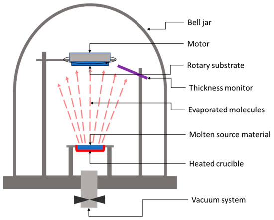
Figure 51.
Schematic representation of a classic thermal evaporation system.
The heated target releases atoms or molecules, which accumulate near the parent surface, forming a vapor cloud. Because of the large temperature difference between the target and the substrate, a temperature gradient occurs, leading to a stream of the vapor from the target to the substrate’s surface. Once the atoms or molecules hit the substrate’s surface, they will condense on it back to a solid state. After applying this deposition method, in 2010, Wang et. al. from IBM reported 6.8% efficiency in Cu2ZnSnS4 solar cells on glass substrates made by thermal evaporation of Cu, Zn, Sn, and S [30][3]. Later on, in 2011, Shin et al. from IBM reported a solar cell efficiency of 8.4% for a solar sell based on 600-nm-thick CZTS layers of Cu, Zn, Sn and S deposited by thermal co-evaporation at 150 °C, followed by 5 min high-temperature annealing (570 °C) of the deposited layer under atmospheric pressure [50][4]. It is worth noting that Shin et al.’s reported efficiency values were independently confirmed and certified by an external, accredited laboratory, i.e., The Newport Technology and Applications Center’s Photovoltaic Laboratory, as having the worldwide record efficiency for pure sulfide CZTS absorbers using any technique at that time.
Through use of a thermal co-evaporation method, a certified power conversion efficiency of 11.6% for a pure Cu2ZnSnSe4 solar cell and a significant improvement in the open-circuit deficit of 0.578 V was reported by Lee et al. [51][5].
2.2. Sputtering Methods
Sputtering is a physical deposition method used to growth thin films on a substrate in a vacuum chamber filled with a chemically inert gas, usually argon. Figure 62 shows the conceptual layout of the DC sputtering system usually involved in the deposition of CZTS films.
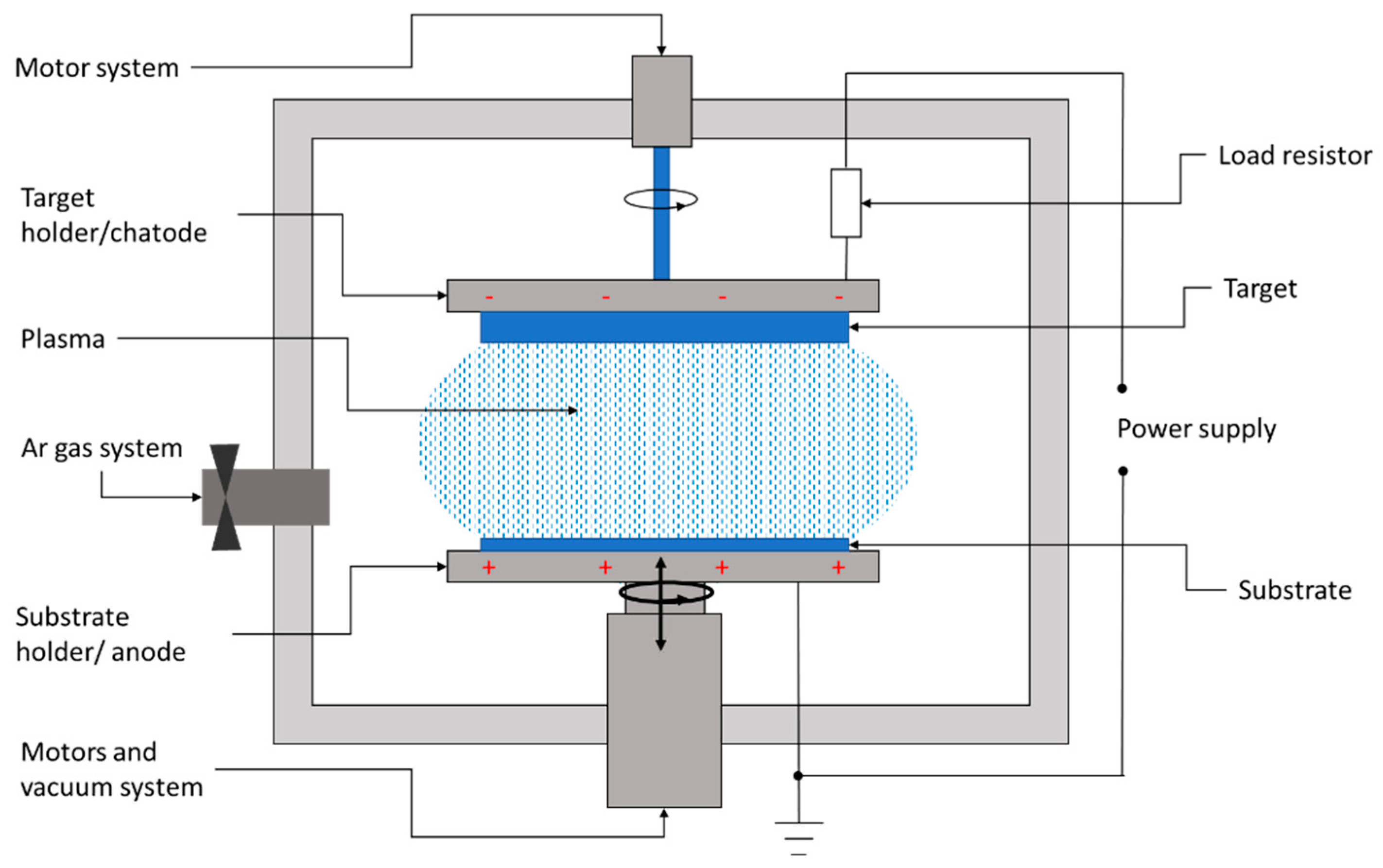
Figure 62.
Layout of a DC sputtering system for the deposition of thin films.
The sputtering system consists of a high-vacuum chamber, inside which is a pair of electrodes. The top electrode is covered with the material to be transferred, also called the target, while the bottom electrode represents the substrate holder.
In between the target and substrate, a voltage source is applied, with the negative polarity on the target. Thus, the target becomes a cathode liberating electrons. These electrons collide with the outer electrons surrounding the gas atom, and thus, a hot gas-like plasma phase consisting of ions and electrons is promoted. Once the electrons have been lost, the neutral atom turns into a high-energy ion. The negatively charged source material attracts these positive ions, which fly at it with such high velocity that atomic-sized particles are “sputtered off,” or detached. The positively charged ions thus formed are accelerated to the target and strike with sufficient kinetic energy to dislodge the atoms or molecules of the target material. The liberated atoms or molecules will fly to the substrate’s surface. When a large number of atoms collide on the substrate, they start to form a bond with each other at the molecular level, leading to the growth of a thin film with the same composition as the target material.
The first use of the sputtering method to fabricate CZTS absorbers was reported by Ito et al. in 1988. The authors sputtered a CZTS film from the target material by applying the method of atomic beam sputtering and obtained a CZTS film with a 1.45 eV optical bandgap and an VOC of 165 mV under AM1.5 illumination, without a post-deposition sulfurization treatment and even at a very low substrate temperature of 90 °C [37][6]. Later on, Ito et al. reported an improvement in the open-circuit voltage to 265 mV by annealing the device in air [52][7]. In 2007, a 5.74% conversion efficiency was reported by Jimbo et al. for a solar cell based on 480 nm high-quality CZTS films fabricated at a Cu/(Zn + Sn) ratio of 0.87 in a co-sputtering system with three RF sources followed by vapor phase sulfurization [53][8]. The record laboratory-reported efficiency was reported by Yan et al. [54][9]. The authors deposited sulfide kesterite CZTS precursors by co-sputtering Cu/ZnS/SnS material using a magnetron sputtering system. The final CZTS films were synthesized by sulfurization of the precursors within a combined sulfur and a SnS atmosphere by rapid thermal annealing at 560 °C for three minutes. The authors demonstrated efficient sulfide kesterite CZTS solar cells with 11% for cells with a small area (0.23 cm2) and 10% for a standard-sized cell (1.11 cm2).
2.3. Pulsed Laser Deposition
Pulsed laser deposition (PLD) is a simple and versatile vacuum-based technique for depositing thin films of a wide range of materials on a wide variety of substrates at temperatures starting from room temperature. The PLD technique offers some unique features such a high deposition rate, relatively easier transfer of species from the target to the substrate, growth from an energetic beam, and reactive deposition. The PLD technique is used to grow engineered layered materials with a controlled thickness and metastable phases [55][10].
As shown in Figure 73, the PLD system consists of a high-vacuum chamber in which a high-powered laser beam of a certain energy density is focused on a rotating target. The extreme energy (1 ÷ 5 J/cm2) of the focused beam is absorbed by the target’s surface area, leading to the breakdown of chemical bonds within the target material. Consequently, ions, electrons, atoms, radicals, or clusters are ejected from the target’s surface, leading to the formation of a so-called ablation plume. These released species traveling at high speed (around 106 cm/s) through the vacuum chamber until they collide at high impact energies (typically 100 eV) on the substrate’s surface. The as-landed particles start to form chemical bonds with each other at the molecular level, forming a continuous thin film with the same composition as the target material [55,56][10][11]. Further laser pulses ablate more material, and the growing layer’s thickness will increase from monolayers up to microns. The layers grow through diffusion and particle aggregation, which improves the layer-by-layer growth [55,57][10][12]. According to the literature, the laser type most commonly used to fabricate CZTS absorber layers are excimer lasers and Nd:YAG lasers.
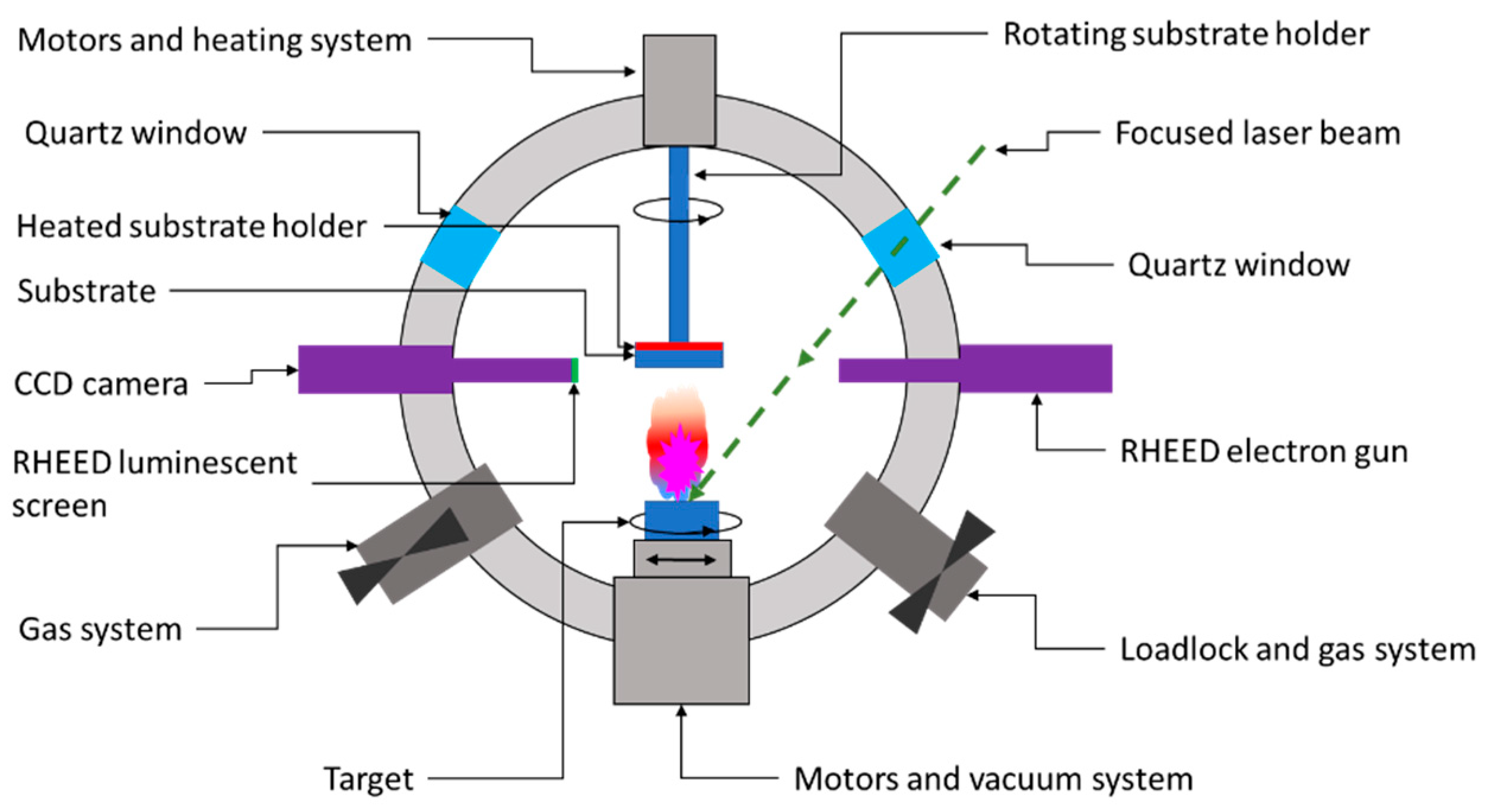
Figure 73.
Schematic representation of a PLD deposition chamber.
Despite the unique beneficial features offered by the PLD in terms of the high-quality growth layer, the literature does not abound in reported results about the notable performance of CZTS solar cell devices processed by PLD. The PLD equipment is expensive and this strongly restricts the marketability of PLD-manufactured photovoltaic devices.
The first CZTS thin-film solar cell prepared by PLD was reported in 2007 by Moriya et al. The authors reported a VOC of 546 mV and a conversion efficiency of 1.74% for their solar cell based on an absorber CZTS synthetized by PLD at 500 °C in N2. Moholkar et al. [58][13] synthetized thin films of CZTS by PLD that were used as an absorber layer in a solar cell configuration. The fabricated solar cell exhibited an open-circuit voltage of 585 mV and a conversion efficiency of 2.02%. Using the PLD technique, in 2012, the same group of authors reported the impact of the chemical composition ratio of the target Cu/(Zn + Sn) on the performance of the final solar cell device. They found that by increasing the Cu/(Zn + Sn) ratio from 0.8 to 1.2 while keeping the Zn/Sn constant, the direct bandgap energy of the CZTS absorber decreased from 1.72 eV to 1.53 eV. The best performances reported by the authors were a conversion efficiency of 4.13% and VOC = 700 mV on a glass/Mo/CZTS/CdS/ZnO:Al/Al solar cell fabricated by using Cu/(Zn + Sn) = 1.1 [59,60,61][14][15][16].
3. Chemical Methods
The chemical methods of depositing thin films are the most economically attractive and versatile techniques for growing sulfide and oxide layers. The most notable features of this method are its ease of handling, the simplicity of the process, the compact low-cost equipment, and low wastage of the precursor materials. However, some critical issues have to be addressed when the chemical deposition methods of absorber CZTS layers are used, such as the need for multiple uniform coatings, uniformity, and cracks.
The current record for the efficiency of CZTS solar cells (12.6%) was found for a CZTS absorber layer processed by the chemical solution approach using hydrazine as a solvent [3][1]. As this solvent is hazardous, reactive, and unstable, the hydrazine-based chemical method is not attractive to the industry for large-scale CZTS solar cell fabrication.
3.1. Sol-Gel Method
Sol-gel, based on the spin coating technique, is a simple and cost-efficient approach to the preparation of various thin oxide films. This method is very attractive for mass-production because of its easy handling and its suitability for large-area deposition, and because no vacuum system is required, allowing thermal annealing in air at temperatures as low as room temperature. Another remarkable feature of the sol-gel synthesis method is that this technology is suitable for the synthesis of high-yield, high-quality solar cells made from thin CZTS thin films through inexpensive green processes, making it very attractive for large-scale industrialization [62,63][17][18]. However, some issues are related to this method; for example, it is a time-consuming process and controlling the porosity of the growing layer is quite difficult.
The sol-gel method consists of three main steps, i.e., (i) preparation of the precursor solution and spin-coating the precursor solution onto the substrate, (ii) the low-temperature thermal treatment, and (iii) the final high temperature annealing. Figure 84 shows a typical set-up of synthesizing the CZTS precursor solution.
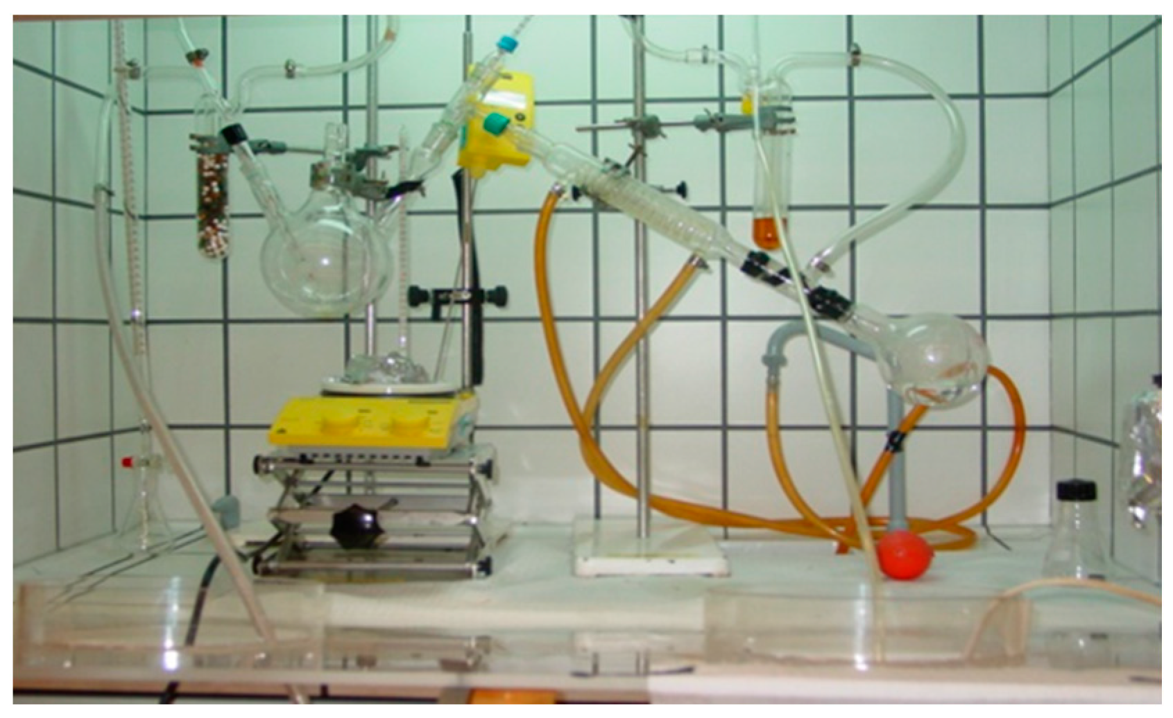
Figure 84.
Installation used for the synthesis of the CZTS precursor solution at the authors’ facilities.
The CZTS precursor solution is synthetized by dissolving the elements raw precursors in 2-methoxyethanol (C3H8O2), i.e., a salt of copper (for Cu), a salt of zinc (for Zn), a salt of tin (for Sn), and thiourea (NH2)2CS (for S). The 2-methoxyethanol solvent removes the necessity to perform prolonged low-temperature processing of the deposited solution on the substrate after spin-coating (110 °C ÷ 120 °C temperature annealing for 80 ÷ 120 min), which not only significantly increases the fabrication time of the CZTS film at the optimal thickness (around 1 µm) but also favors the formation of undesirable oxide compounds in CZTS films, and thus results in the low reproducibility of the electrical and optical parameters [64,65,66,67][19][20][21][22]. Dimethyl sulfoxide (DMSO) has been successfully used for the synthesis of the precursor solution and spin-coating of CZTS films. The most prominent features of the DMSO solvent relate to its green technology approach, its non-toxic character, the high yield, and the low cost [67][22].
Tanaka et al. synthesized CZTS films by spin-coating a sol-gel precursor solution based on copper (II) acetate monohydrate, zinc (II) acetate dehydrate, and tin (II) chloride dehydrate dissolved in a mixed solution of a 2-methoxyethanol (2-metho) solvent and a monoethanolamine (MEA) stabilizer [68][23]. Thin CZTS films were grown by annealing the precursor films in an atmosphere containing H2S at 500 °C. The fabricated CZTS solar cells had an open-circuit voltage of 390 mV and an efficiency of 1.01%. The same group of authors investigated the impact of the precursor solution’s chemical composition on the morphology and the photovoltaic performance of the thin CZTS films fabricated by the sol-gel spin-coating technique. The authors varied the Cu/(Zn + Sn) ratio in precursor solution of the sol-gel while keeping the Zn/Sn ratio constant at 1.15 [69][24]. According to the results reported by Tanaka, large grains characterized the films made from the copper-poor precursor solution (Cu/(Zn + Sn) < 0.8, molar ratio). The best solar cell had a VOC of 575 mV and an efficiency of 2.03%. Agawane et al. reported achieving a 0.77% conversion efficiency with a solar cell fabricated from a CZTS absorber layer synthetized by the sol-gel technique annealed under S powder [70][25]. Later on, the same group of authors reported an improvement in the processing conditions and achieved a conversion efficiency of 3.01% with a solar cell based on a CZTS absorber layer prepared by a non-toxic, simple, and economical sol-gel and spin-coating technique annealed at 550 °C under a H2S gas atmosphere [62][17]. Using non-aqueous thiourea–metal–oxygen sol-gel processing, Su et al. synthetized high-quality phase-controlled CZTS layers with a homogeneous elemental distribution and a low impurity content by introducing Na as an extrinsic dopant [63][18]. Through use of this modified sol-gel method, the fabricated Ni:Al/ZAO/i-ZnO/CdS/1%Na:CZTS/Mo/glass solar cells achieved a power conversion efficiency of 5.10%, while the device without Na had an efficiency of only 4.10%. The authors reported that a further improvement in the conversion efficiency of up to 5.10% was obtained by HCl chemical etching of the CZTS absorber layer. Liu et al. used the sol-gel and selenization processes and fabricated high-quality single-phase kesterite CZTSSe with a total area efficiency of 8.5% without an antireflection coating [71][26]. The sol-gel method was also used in the study performed by Sun et al. to fabricate solar cells based on CZTS absorbers [72][27]. The authors tuned the Cu/Sn with the purpose of improving the films’ uniformity, reducing the formation of voids, and enhancing the power conversion efficiency. The best cell achieved an efficiency of 8.8% with an open-circuit voltage of 746 mV. Todorov et al. processed CZTS films by spin-coating deposition of a precursor solution of a slurry of hydrazine and particles of the Cu, Zn, Sn, and S elements. The spin-coated CZTS precursor thin films were annealed at 540 °C in an atmosphere containing sulfoselenide, and the best measured efficiency was 9.66% [73][28]. In 2013, Wang et al. all reported the results of their own approach involving the liquid deposition of thin CZTS films based on a pure solution of hydrazine [3][1]. The reported results were independently certified and the conversion efficiency of 12% they achieved represents the world-record power conversion efficiency for CZTSSe thin films. The new device’s open-circuit voltage was 513.4 mV.
3.2. The Solvothermal Method
The solvothermal method is a chemical process in which the chemical reaction between the involved precursors take place in a solvent sealed in a vessel heated above the solvent’s boiling temperatures (usually less than 250 °C). The sealed reaction vessel, also called an autoclave, acts as a closed system in which the elevated temperature and pressure promote the reactivity of the reactants, leading to the formation of a supercritical fluid in which the gas and liquid phases coexist, favoring the crystallization of the dissolved raw precursors. The solvothermal reaction products are homogenous high-purity nanosized particles. The products’ shape and size are controlled through the reaction temperature, solvent, and pH. The solvothermal method does not require post-synthesis annealing processes of the resulting products. The resulting nanoparticles are further used to grow thin films. In this method, the working substrate is immersed in a mixed solution of the solvent and the solvothermal products dissolved in it. After dipping, the covered substrate is dried in order to remove the solvent. The thin films grown by the solvothermal method have good uniformity, high crystallinity, and a stable structure. The main factors affecting the thin films’ growth are: (i) the nature of solvent, (ii) the temperature, (iii) the time, (iv) the concentration of the precursor material, (v) the concentration of OH− ions in the solution, and (vi) the pH. One of the most notable features of the thin films fabricated by the solvothermal method is the low-temperature growing process that reduces the possibility of chemical reactions between the substrate and the reactants. Other benefits offered by the solvothermal method of synthesizing CZTS absorbers include its ease of use, and its accurately and reliability in synthesizing high-purity and highly crystalline materials. This method is considered to be a green technology that is suitable for mass production of good-quality crystals while maintaining the control over their composition and morphology [74][29].
Several research groups have reported results for CZTS-based solar cells fabricated by the solvothermal method [75,76,77,78][30][31][32][33]. To obtain CZTS absorber layers, firstly the solvothermally synthesized CZTS nanoparticles are dispersed in solvents to create a paste or ink. The as-obtained slurry is deposited on the working substrate by printing, spraying, or dip-coating, followed by a high-temperature thermal annealing treatment to ensure the formation of the crystalline phase [79,80][34][35].
Wei et al. used the solvothermal method to grow Cu2ZnSnS4 (CZTS) layers directly on transparent conductive fluorine-doped tin oxide (FTO) substrates using hexadecyl trimethyl ammonium bromide (CTAB) as the surfactant [81][36]. The fabricated glass/FTO/CZTS/CdS/i-ZnO/AleZnO/Ag solar cells were characterized by an optical bandgap of 1.52 eV and a poor power conversion efficiency of only 0.16%. Using the solvothermal method, Al-Hadeethi et al. studied the impact of the concentration of triethanolamine (TEA) on the structure, phase formation, morphology, and composition of the resulting CZTS nanoparticles [78][33]. The authors fabricated a SLG/Mo/CZTS/CdS/i-ZnO/Al:ZnO/Al structure using CZTS particles synthesized with a TEA concentration of 5 mg/mL, and the best demonstrated solar conversion efficiency was reported to be 4.33%. In a recent study published by Kannan et al., the authors used ethylene glycol (EG) as a solvent and investigated the impact of the Cu/(Zn + Sn) ratio on the properties of the CZTS nanoparticles synthesized by the solvothermal method [82][37]. The synthetized nanocrystals were used to fabricate a CZTS/ZnO photovoltaic structure from a scalpel-cut absorber and a drop-cast ZnO buffer layer. The authors reported that the devices based on absorber layers that were slightly poor in Cu (0.9) provided the best open-circuit voltage (510 mV), short circuit current (11.49 mA/cm2), filing factor (52.97%), and power conversion efficiency (3.2%).
References
- Wang, W.; Winkler, M.T.; Gunawan, O.; Gokmen, T.; Todorov, T.K.; Zhu, Y.; Mitzi, D.B. Device Characteristics of CZTSSe Thin-Film Solar Cells with 12.6% Efficiency. Adv. Energy Mater. 2014, 4, 1301465.
- Mora-Herrera, D.; Silva-González, R.; Cancino-Gordillo, F.E.; Pal, M. Development of Cu2ZnSnS4 Films from a Non-Toxic Molecular Precursor Ink and Theoretical Investigation of Device Performance Using Experimental Outcomes. Sol. Energy 2020, 199, 246–255.
- Wang, K.; Gunawan, O.; Todorov, T.; Shin, B.; Chey, S.J.; Bojarczuk, N.A.; Mitzi, D.; Guha, S. Thermally Evaporated Cu2ZnSnS4 Solar Cells. Appl. Phys. Lett. 2010, 97, 143508.
- Shin, B.; Gunawan, O.; Zhu, Y.; Bojarczuk, N.A.; Chey, S.J.; Guha, S. Thin Film Solar Cell with 8.4% Power Conversion Efficiency Using an Earth-Abundant Cu2ZnSnS4 Absorber. Prog. Photovolt. Res. Appl. 2013, 21, 72–76.
- Lee, Y.S.; Gershon, T.; Gunawan, O.; Todorov, T.K.; Gokmen, T.; Virgus, Y.; Guha, S. Cu2ZnSnSe4 Thin-Film Solar Cells by Thermal Co-Evaporation with 11.6% Efficiency and Improved Minority Carrier Diffusion Length. Adv. Energy Mater. 2015, 5, 1401372.
- Nakazawa, K.I. Electrical and Optical Properties of Stannite-Type Quaternary Semiconductor Thin Films. Jpn. J. Appl. Phys. 1988, 27, 2094.
- Ito, K. (Ed.) Copper Zinc Tin Sulfide-Based Thin-Film Solar Cells; Wiley: Hoboken, NJ, USA, 2014.
- Jimbo, K.; Kimura, R.; Kamimura, T.; Yamada, S.; Maw, W.S.; Araki, H.; Oishi, K.; Katagiri, H. Cu2ZnSnS4-Type Thin Film Solar Cells Using Abundant Materials. Thin Solid Films 2007, 515, 5997–5999.
- Yan, C.; Huang, J.; Sun, K.; Johnston, S.; Zhang, Y.; Sun, H.; Pu, A.; He, M.; Liu, F.; Eder, K.; et al. Cu2ZnSnS4 Solar Cells with over 10% Power Conversion Efficiency Enabled by Heterojunction Heat Treatment. Nat. Energy 2018, 3, 764–772.
- Vanalakar, S.A.; Agawane, G.L.; Shin, S.W.; Suryawanshi, M.P.; Gurav, K.V.; Jeon, K.S.; Patil, P.S.; Jeong, C.W.; Kim, J.Y.; Kim, J.H. A Review on Pulsed Laser Deposited CZTS Thin Films for Solar Cell Applications. J. Alloys Compd. 2015, 619, 109–121.
- Lowndes, D.H.; Geohegan, D.B.; Puretzky, A.A.; Norton, D.P.; Rouleau, C.M. Synthesis of Novel Thin-Film Materials by Pulsed Laser Deposition. Science 1996, 273, 898–903.
- Vasco, E.; Sacedón, J.L. Role of Cluster Transient Mobility in Pulsed Laser Deposition-Type Growth Kinetics. Phys. Rev. Lett. 2007, 98, 36104.
- Moholkar, A.V.; Shinde, S.S.; Babar, A.R.; Sim, K.-U.; Kwon, Y.; Rajpure, K.Y.; Patil, P.S.; Bhosale, C.H.; Kim, J.H. Development of CZTS Thin Films Solar Cells by Pulsed Laser Deposition: Influence of Pulse Repetition Rate. Sol. Energy 2011, 85, 1354–1363.
- Reyes-Banda, M.G.; Regalado-Perez, E.; Pintor-Monroy, M.I.; Hernández-Gutiérrez, C.A.; Quevedo-López, M.A.; Mathew, X. Effect of Se Diffusion and the Role of a Thin CdS Buffer Layer in the Performance of a CdSe/CdTe Solar Cell. Superlattices Microstruct. 2019, 133, 106219.
- Liang, G.-X.; Luo, Y.-D.; Hu, J.-G.; Chen, X.-Y.; Zeng, Y.; Su, Z.-H.; Luo, J.-T.; Fan, P. Influence of Annealed ITO on PLD CZTS Thin Film Solar Cell. Surf. Coatings Technol. 2019, 358, 762–764.
- Gutierrez, Z.-B.K.; Zayas-Bazán, P.G.; de Moure-Flores, F.; Jiménez-Olarte, D.; Sastré-Hernández, J.; Hernández-Gutiérrez, C.A.; Aguilar-Hernández, J.R.; Mejía-García, C.; Morales-Acevedo, A.; Contreras-Puente , G. Development of a CdCl2 Thermal Treatment Process for Improving CdS/CdTe Ultrathin Solar Cells. J. Mater. Sci. Mater. Electron. 2019, 30, 16932–16938.
- Agawane, G.L.; Kamble, A.S.; Vanalakar, S.A.; Shin, S.W.; Gang, M.G.; Yun, J.H.; Gwak, J.; Moholkar, A.V.; Kim, J.H. Fabrication of 3.01% Power Conversion Efficient High-Quality CZTS Thin Film Solar Cells by a Green and Simple Sol–Gel Technique. Mater. Lett. 2015, 158, 58–61.
- Su, Z.; Sun, K.; Han, Z.; Cui, H.; Liu, F.; Lai, Y.; Li, J.; Hao, X.; Liu, Y.; Green, M.A. Fabrication of Cu2ZnSnS4 Solar Cells with 5.1% Efficiency via Thermal Decomposition and Reaction Using a Non-Toxic Sol–Gel Route. J. Mater. Chem. A 2014, 2, 500–509.
- Yu, X.; Ren, A.; Wang, F.; Wang, C.; Zhang, J.; Wang, W.; Wu, L.; Li, W.; Zeng, G.; Feng, L. Synthesis and Characterization of CZTS Thin Films by Sol-Gel Method without Sulfurization. Int. J. Photoenergy 2014, 2014, 861249.
- Ashfold, M.N.R.; Claeyssens, F.; Fuge, G.M.; Henley, S.J. Pulsed Laser Ablation and Deposition of Thin Films. Chem. Soc. Rev. 2004, 33, 23–31.
- Majula, L.; Mlyuka, N.R.; Samiji, M.E.; Bryce, R.S.; Kim, D.Y.; Kim, S.H.; Lee, H.J.; Choi, H.J. Spin-Coated Kesterite CZTS Thin Films for Photovoltaic Applications. J. Korean Phys. Soc. 2015, 67, 1078–1081.
- Orletskyi, I.G.; Solovan, M.M.; Brus, V.V.; Pinna, F.; Cicero, G.; Maryanchuk, P.D.; Maistruk, E.V.; Ilashchuk, M.I.; Boichuk, T.I.; Tresso, E. Structural, Optical and Electrical Properties of Cu2ZnSnS4 Films Prepared from a Non-Toxic DMSO-Based Sol-Gel and Synthesized in Low Vacuum. J. Phys. Chem. Solids 2017, 100, 154–160.
- Tanaka, K.; Oonuki, M.; Moritake, N.; Uchiki, H. Cu2ZnSnS4 Thin Film Solar Cells Prepared by Non-Vacuum Processing. Sol. Energy Mater. Sol. Cells 2009, 93, 583–587.
- Tanaka, K.; Fukui, Y.; Moritake, N.; Uchiki, H. Chemical Composition Dependence of Morphological and Optical Properties of Cu2ZnSnS4 Thin Films Deposited by Sol–Gel Sulfurization and Cu2ZnSnS4 Thin Film Solar Cell Efficiency. Sol. Energy Mater. Sol. Cells 2011, 95, 838–842.
- Agawane, G.L.; Shin, S.W.; Vanalakar, S.A.; Suryawanshi, M.P.; Moholkar, A.V.; Yun, J.H.; Gwak, J.; Kim, J.H. Synthesis of Simple, Low Cost and Benign Sol–Gel Cu2ZnSnS4 Thin Films: Influence of Different Annealing Atmospheres. J. Mater. Sci. Mater. Electron. 2015, 26, 1900–1907.
- Liu, F.; Zeng, F.; Song, N.; Jiang, L.; Han, Z.; Su, Z.; Yan, C.; Wen, X.; Hao, X.; Liu, Y. Kesterite Cu2ZnSn(S,Se)4 Solar Cells with beyond 8% Efficiency by a Sol–Gel and Selenization Process. ACS Appl. Mater. Interfaces 2015, 7, 14376–14383.
- Sun, K.; Yan, C.; Liu, F.; Hao, X. Towards 9% Sulfide CZTS Solar Cells Fabricated by a Sol-Gel Process. In Proceedings of the 2018 IEEE 7th World Conference on Photovoltaic Energy Conversion (WCPEC) (A Joint Conference of 45th IEEE PVSC, 28th PVSEC & 34th EU PVSEC), Waikoloa Village, HI, USA, 10–15 June 2018; pp. 856–858.
- Todorov, T.K.; Reuter, K.B.; Mitzi, D.B. High-Efficiency Solar Cell with Earth-Abundant Liquid-Processed Absorber. Adv. Mater. 2010, 22, E156–E159.
- Kannan, A.G.; Manjulavalli, T.E.; Chandrasekaran, J. Influence of Solvent on the Properties of CZTS Nanoparticles. Procedia Eng. 2016, 141, 15–22.
- Kamalanathan, M.; Shamima, H.; Gopalakrishnan, R.; Vishista, K. Influence of Solvents on Solvothermal Synthesis of Cu2SnS3 Nanoparticles with Enhanced Optical, Photoconductive and Electrical Properties. Mater. Technol. 2018, 33, 72–78.
- Dumasiya, A.; Shah, N.M. Solvothermal Synthesis and Characterization of CZTS Nanocrystals. AIP Conf. Proc. 2017, 1837, 40067.
- Mkawi, E.M.; Al-Hadeethi, Y.; Shalaan, E.; Bekyarova, E. Fabricating Chalcogenide Cu2ZnSnS4 (CZTS) Nanoparticles via Solvothermal Synthesis: Effect of the Sulfur Source on the Properties. Ceram. Int. 2020, 46, 24916–24922.
- Al-Hadeethi, Y.; Mkawi, E.M.; Al-Hartomy, O.; Bekyarova, E. Role of Triethanolamine in Forming Cu2ZnSnS4 Nanoparticles during Solvothermal Processing for Solar Cell Applications. Int. J. Energy Res. 2022, 46, 7239–7248.
- Camara, S.M.; Wang, L.; Zhang, X. Easy Hydrothermal Preparation of Cu2ZnSnS4 (CZTS) Nanoparticles for Solar Cell Application. Nanotechnology 2013, 24, 495401.
- Oliveira, L.; Todorov, T.; Chassaing, E.; Lincot, D.; Carda, J.; Escribano, P. CIGSS Films Prepared by Sol–Gel Route. Thin Solid Films 2009, 517, 2272–2276.
- Wei, A.; Yan, Z.; Zhao, Y.; Zhuang, M.; Liu, J. Solvothermal Synthesis of Cu2ZnSnS4 Nanocrystalline Thin Films for Application of Solar Cells. Int. J. Hydrogen Energy 2015, 40, 797–805.
- Kannan, G.; Manjulavalli, T.E.; Thambidurai, M.; Habeeba, K.; Ezhilarasi GnanaKumari, D. V 3.2% Efficient Cadmium Free Cu2ZnSnS4/ZnO Solar Cells Fabricated Using Solvothermally Synthesized Nanoparticles. IOP Conf. Ser. Mater. Sci. Eng. 2022, 1219, 12036.
More