Your browser does not fully support modern features. Please upgrade for a smoother experience.
Please note this is a comparison between Version 2 by Antonio Aprile and Version 1 by Antonio Aprile.
On-chip tTemperature measurements have acquired an increasingly important role over the past two decades, especially considering-to-Digital Converters (TDCs) are on-chip sensors that produce data in the digital domain, referred to as Tgenerate temperature-to-Ddependent digital Converters (TDCs)codes.
- temperature
- TDCs
- smart sensors
- integrated circuits
1. Introduction
On-chip temperature measurements have acquired an increasingly important role over the past two decades, especially if we consider sensors that produce data in the digital domain, referred to as Temperature-to-Digital Converters (TDCs). The growing computational power of modern microprocessors has given rise to a higher degree of criticality in their thermal management process [1]; for instance, dynamic voltage and frequency scaling (DVFS), a commonly used approach in this framework [2], requires responsive temperature tracking to allow an effective control on the thermal status of the microprocessor and, furthermore, the cooling fans’ speed regulation is also based on a continuous temperature monitoring [3,4,5]. Another field that has featured a remarkable growth in recent years is the Micro-Electro-Mechanical Systems (MEMS) one [6]; the employment of these devices for Internet of Things (IoT) applications, supported by a parallel technological development, has led the research focus to more and more robust devices with respect to the influence of environmental effects. One of the main challenges is, indeed, to mitigate the impact of the ambient temperature on the performance of these devices; the micro-structures used as sensing elements suffer from a significant thermal spread causing a degradation of the reliability of the sensed quantity. For this reason, high-precision MEMS devices also require a temperature tracking to compensate for the drift of their parameters [7,8,9,10,11]. Integrated temperature sensors are also used for clinical applications [12,13,14]; devices that provide a high accuracy monitoring in the human body temperature range are needed for the detection of atypical biomedical conditions. Lastly, since temperature is a fundamental physical parameter of both industry and everyday life, on-chip temperature measurements are also combined with radio-frequency identification (RFID) tags in several applications: monitoring of the food cold chain [15,16], environmental monitoring [17,18], supply chain management of healthcare products [19], animal healthcare monitoring [20] and many more.
2. Temperature-to-Digital Converters
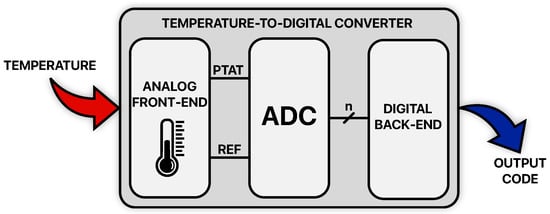
There are a lot of applications requiring on-chip temperature sensing, as seen in the introduction, and concern several systems in the microelectronics field; despite their wide range, all the reported examples [3,4,5,7,8,9,10,11,12,13,14,15,16,17,18,19,20] have one important feature in common: they provide temperature information in the form of digital data. This is fundamental as it makes them compatible for a direct communication with digital signal processing (DSP) circuits that can easily handle the needed temperature information and at the same time reduces the complexity of the system they are inserted in; for this reason, they are often referred to as smart temperature sensors [21] or as Temperature-to-Digital Converters (TDCs). It is important to specify that this category of temperature sensors was born with a cost-minimization perspective and that its development in the past two decades has consequently followed this line; even if, in principle, these fully integrated temperature sensors have significant limitations in terms of accuracy and sensing range with respect to other existing discrete sensors, their great success is related to their compatibility with large-scale production of low-cost products being integrated within the system in which they are operated. Figure 1 shows the conceptual diagram of a TDC.
Figure 1. Conceptual diagram of a Temperature-to-Digital Converter.
