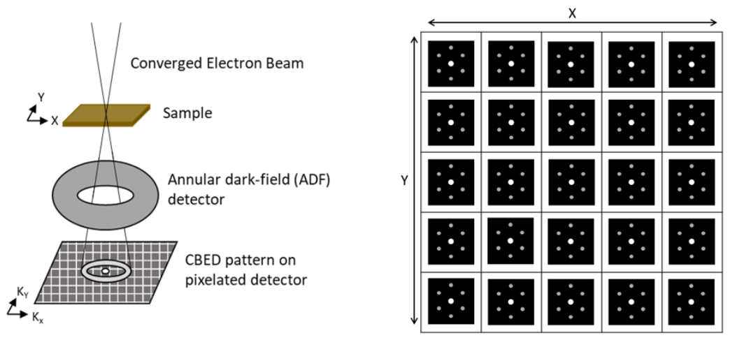
4D scanning transmission electron microscopy (4D STEM) is a subset of scanning transmission electron microscopy (STEM) which utilizes a pixelated electron detector to capture a convergent beam electron diffraction (CBED) pattern at each scan location. This technique captures a 2 dimensional reciprocal space image associated with each scan point as the beam rasters across a 2 dimensional region in real space, hence the name 4D STEM. Its development was enabled by evolution in STEM detectors and improvements computational power. The technique has applications in visual diffraction imaging, phase orientation and strain mapping, phase contrast analysis, among others. The name 4D STEM is common in literature, however it is known by other names: 4D STEM EELS, ND STEM (N- since the number of dimensions could be higher than 4), position resolved diffraction (PRD), spatial resolved diffractometry, momentum-resolved STEM, "nanobeam precision electron diffraction", scanning electron nano diffraction, nanobeam electron diffraction, or pixelated STEM.
- electron diffraction
- scanning electron
- electron microscopy
1. History
One of the earliest instances where the analysis of diffraction patterns as a function of probe position was considered took place in 1995, where Nellist, McCallum and Rodenburg attempted electron Ptychography analysis of crystalline Silicon.[1]
The fluctuation electron microscopy (FEM) technique, proposed in 1996 by Treacy and Gibson, also included quantitative analysis of the differences in images or diffraction patterns taken at different locations on a given sample.[2]
The field of 4D STEM remained underdeveloped due to the limited capabilities of detectors available at the time. CCD detectors commonly used in transmission electron microscopy (TEM) had limited data acquisition rates, could not distinguish where on the detector an electron strikes with high accuracy, and had low dynamic range which made them undesirable for use in 4D STEM.[3]
In the late 2010s, the development of hybrid pixel array detectors (PAD) with single electron sensitivity, high dynamic range, and fast readout speeds allowed for practical 4D STEM experiments.[4][5]
2. Operating Principle
While the process of data collection in 4D STEM is identical to that of standard STEM, each technique utilizes different detectors and collects different data. In 4D STEM there is a pixelated electron detector located at the back focal plane which collects the CBED pattern at each scan location. An image of the sample can be constructed from the CBED patterns by selecting an area in reciprocal space and assigning the average intensity of that area in each CBED pattern to the real space pixel the pattern corresponds to.
It is also common for there to be a(n) ADF or HAADF image taken concurrently with the CBED pattern collection. The dark-field image taken is complementary to the bright-field image constructed from the captured CBED images.
The use of a hollow detector with a hole in the middle can allow for transmitted electrons to be passed to an EELS detector while scanning. This allows for the simultaneous collection of chemical spectra information and structure information.
3. Detectors
In traditional TEM, imaging detectors use phosphorescent scintillators paired with a charge coupled device (CCD) to detect electrons.[6] While these devices have good electron sensitivity, they lack the necessary readout speed and dynamic range necessary for 4D STEM. Additionally, the use of a scintillator can worsen the point spread function (PSF) of the detector due to the electron's interaction with the scintillator resulting in a broadening of the signal. In contrast, traditional annular STEM detectors have the necessary readout speed, but instead of collecting a full CBED pattern the detector integrates the collected intensity over a range of angles into a single data point.[7] The development of pixelated detectors in the 2010s with single electron sensitivity, fast readout speeds, and high dynamic range has enabled 4D STEM as a viable experimental method.[3]
4D STEM detectors are typically built as either a monolithic active pixel sensor (MAPS) or as a hybrid pixel array detector (PAD).[3]
3.1. Monolithic Active Pixel Sensor (MAPS)
A MAPS detector consists of a complimentary metal-oxide-semiconductor (CMOS) chip paired with a doped epitaxial surface layer which converts high energy electrons into many lower energy electrons that travel down to the detector. MAPS detectors must be radiation hardened as their direct exposure to high energy electrons makes radiation damage a key concern.[8]
Due to its monolithic nature and straightforward design, MAPS detectors can attain high pixel densities on the order of 4000 x 4000. This high pixel density when paired with low electron doses can enable single electron counting for high efficiency imaging. Additionally, MAPS detectors tend to have electron high sensitivities and fast readout speeds, but suffer from limited dynamic range.[9]
3.2. Pixel Array Detector (PAD)
PAD detectors consist of a photodiode bump bonded to an integrated circuit, where each solder bump represents a single pixel on the detector.[4]
These detectors typically have lower pixel densities on the order of 128 x 128 but can achieve much higher dynamic range on the order of 32 bits. These detectors can achieve relatively high readout speeds on the order of 1 ms/pixel but are still lacking compared to their annular detector counterparts in STEM which can achieve readout speeds on the order of 10 μs/pixel.[4][5][10]
Detector noise performance is often measured by its detective quantum efficiency (DQE) defined as: [math]\displaystyle{ DQE=\frac{SNR_o^2}{SNR_i^2} }[/math]
Where [math]\displaystyle{ SNR_o^2 }[/math] is output signal to noise ratio squared and [math]\displaystyle{ SNR_i^2 }[/math] is the input signal to noise ratio squared. Ideally the DQE of a sensor is 1 indicating the sensor generates zero noise. The DQE of MAPS, APS and other direct electron detectors tend to be higher than their CCD camera counterparts.[11][12]
4. Computational Methods
A major issue in 4D STEM is the large quantity of data collected by the technique. With upwards of 100s of TB of data produced over the course of an hour of scanning, finding pertinent information is challenging and requires advanced computation.[13]
Analysis of such large datasets can be quite complex and computational methods to process this data are being developed. Many code repositories for analysis of 4D STEM are currently in development including: HyperSpy, pyXem, LiberTEM, Pycroscopy, and py4DSTEM.[3][14][15][16][17][18]
These large data sets could enable the implementation of artificial intelligence (AI) and machine learning (ML) algorithms into TEM experiments, where patterns not normally considered by microscopists could be revealed by AI. When grounded in physically meaningful frameworks, AI and ML can lead to high efficiency in feature finding in large STEM datasets. Beyond feature identification, AI and ML can also help inform experimental design due to its effective predictive cost analysis.[19]
These types of AI driven analysis, however, require databases of information to train on which currently do not exist. Additionally, lack of metrics for data quality, limited scalability due to poor cross-platform support across different manufacturers, and lack of standardization in analysis and experimental methods brings up questions of comparability across different datasets as well as reproducibility.[13]
5. Selected Applications
4D STEM has been utilized in a wide array of applications, the most common uses include virtual diffraction imaging, orientation and strain mapping, and phase contrast analysis which are covered below. The technique has also been applied in: medium range order measurement, Higher order Laue zone (HOLZ) channeling contrast imaging, Position averaged CBED, fluctuation electron microscopy, biomaterials characterization, and medical fields (microstructure of pharmaceutical materials and orientation mapping of peptide crystals). This list is in no way exhaustive and as the field is still relatively young more applications are actively being developed.
5.1. Virtual Diffraction Imaging
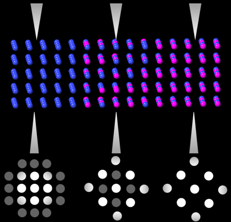
Virtual diffraction imaging is a method developed to generate real space images from diffraction patterns.[3] This technique has been used in characterizing material structures since the 90s[20] but more recently has been applied in 4D STEM applications. This technique is often referred to as scanning electron nano diffraction (SEND) in which 4 pairs of magnetic coils are used to tilt the converged probe and raster the beam across the surface.[21] A "virtual detector," is not a detector at all but rather a method of data processing which integrates a subset of pixels in diffraction patterns at each raster position to create bright-field and dark-field images. The processing of these images is performed by first averaging the diffraction patterns over all scans. Then a region of interest is selected in the diffraction pattern, a virtual aperture is drawn on the reduced dataset, and the image is constructed using computational methods. This virtual aperture can be any size/shape desired and can be created using the 4D dataset gathered from a single scan.[22] This ability to simulate different apertures is enabled by 4D STEM methods and eliminates a typical weaknesses in conventional STEM operation as STEM bright-field and dark-field detectors are placed at fixed angles and cannot be changed during imaging.[23]
With a 4D dataset bright/dark-field images can be obtained by integrating diffraction intensities from diffracted and transmitted beams respectively.[21] Creating images from these patterns can give nanometer resolution and is typically used to characterize the structure of nanomaterials. These diffraction patterns can be indexed and analyzed for orientation and phase mapping, where real space images can be constructed from scans.[3] The advantages of performing virtual imaging in 4D STEM include: enabling detector geometries not possible in conventional electron microscopy, allowing for specific use of scattered electrons at any angle which hits the detector, improving signal to noise on images, and resistance to sample bending/dynamic scattering events.[23]
4D STEM has been used to map interfaces, select intensity from selected areas of the diffraction plane to form enhanced dark field images,[24] map positions of nanoscale precipitates,[25] create phase maps of beam sensitive battery cathode materials,[26] and measure degree of crystallinity in metal-organic frameworks (MOFs).[27]
5.2. Phase Orientation Mapping
Phase orientation mapping is typically done with electron back scattered diffraction in SEM which can give 2D maps of grain orientation in polycrystalline materials.[28] The technique can also be done in TEM using Kikuchi lines, which is more applicable for thicker samples since formation of Kikuchi lines relies on diffuse scattering being present. Alternatively, in TEM one can utilize precession electron diffraction (PED) to record a large number of diffraction patterns and through comparison to known patterns, the relative orientation of grains in can be determined. 4D STEM can also be used to map orientations, in a technique called Bragg spot imaging. The use of traditional TEM techniques typically results in better resolution than the 4D STEM approach but can fail in regions with high strain as the DPs become too distorted.
In Bragg spot imaging, first correlation analysis method is performed to group diffraction patterns (DPs) using a correlation method between 0 (no correlation) and 1 (exact match); then the DP's are grouped by their correlation using a correlation threshold. A correlation image can then be obtained from each group. These are summed and averaged to obtain an overall representative diffraction template from each grouping. Different orientations can be assigned colors which helps visualize individual grain orientations.[21] With proper tilting and utilizing precession electron diffraction (PED) it is even possible to make 3D tomographic renderings of grain orientation and distribution.[29] Since the technique is computationally intensive, recent efforts have been focused on a machine learning approach to analysis of diffraction patterns.[30][31]
5.3. Strain Mapping
TEM can measure local strains and is often used to map strain in samples using condensed beam electron diffraction CBED.[7] The basis of this technique is to compare an unstrained region of the sample's diffraction pattern with a strained region to see the changes in the lattice parameter. With STEM, the disc positions diffracted from an area of a specimen can provide spatial strain information. The use of this technique with 4D STEM datasets includes fairly involved calculations.[3]
Utilizing SEND, bright and dark field images can be obtained from diffraction patterns by integration of direct and diffracted beams respectively, as discussed previously. During 4D STEM operation the ADF detector can be used to visualize a particular region of interest through a collection of scattered electrons to large angles to correlate probe location with diffraction during measurements.[21] There is a tradeoff between resolution and strain information; since larger probes can average strain measurements over a large volume, but moving to smaller probe sizes gives higher real space resolution. There are ways to combat this issue such as spacing probes further apart than the resolution limit to increase the field of view.[3]
This strain mapping technique has been applied in many crystalline materials and has been extended to semi-crystalline and amorphous materials (such as metallic glasses) since they too exhibit deviations from mean atomic spacing in regions of high strain[3][32]
5.4. Phase Contrast Analysis
Differential Phase Contrast
The differential phase contrast imaging technique (DPC) can be used in STEM to map the local electromagnetic field in samples by measuring the deflection of the electron beam caused by the field at each scan point. Traditionally the movement of the beam was tracked using segmented annular field detectors which surrounded the beam. DPC with segmented detectors has up to atomic resolution.[33] The use of a pixelated detector in 4D STEM and a computer to track the movement of the "center of mass" of the CBED patterns was found to provide comparable results to those found using segmented detectors. 4D STEM allows for phase change measurements along all directions to be measured without the need to rotate the segmented detector to align with specimen orientation.[34] The ability to measure local polarization in parallel with the local electric field has also been demonstrated with 4D STEM.[35]
DPC imaging with 4D STEM is up to 2 orders of magnitude slower than DPC with segmented detectors and requires advanced analysis of large four-dimensional datasets.[36]
Ptychography
The overlapping CBED measurements present in a 4D STEM dataset allow for the construction of the complex electron probe and complex sample potential using the ptychography technique. Ptychographic reconstructions with 4D STEM data were shown to provide higher contrast than ADF, BF, ABF, and segmented DPC imaging in STEM. The high signal-to-noise ratio of this technique under 4D STEM makes it attractive for imaging radiation sensitive specimens such as biological specimens[34] The use of a pixelated detector with a hole in the middle to allow the unscattered electron beam to pass to a spectrometer has been shown to allow ptychographic analysis in conjunction with chemical analysis in 4D STEM.[37]
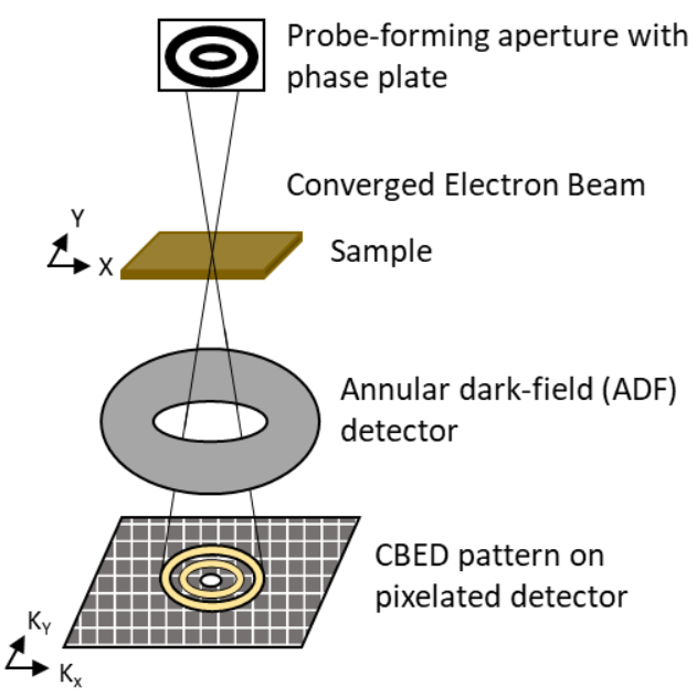
MIDI STEM
This technique MIDI-STEM (matched illumination and detector interferometry-STEM), while being less common, is used with ptychography to create higher contrast phase images. The placement of a phase plate with zones of 0 and π/2 phase shift in the probe forming aperture creates a series of concentric rings in the resulting CBED pattern. The difference in counts between the 0 and π/2 regions allows for direct measurement of local sample phase.[38] The counts in the different regions could be measured via complex standard detector geometries or the use of a pixelated detector in 4D STEM. Pixelated detectors have been shown to utilize this technique with atomic resolution.[39]
(MIDI)-STEM produces image contrast information with less high-pass filtering than DPC or ptychography but is less efficient at high spatial frequencies than those techniques.[3] (MIDI)-STEM used in conjunction with ptychography has been shown to be more efficient in providing contrast information than either technique individually.[40]
References
- Nellist, P. D.; McCallum, B. C.; Rodenburg, J. M. (April 1995). "Resolution beyond the 'information limit' in transmission electron microscopy" (in en). Nature 374 (6523): 630–632. doi:10.1038/374630a0. ISSN 1476-4687. https://www.nature.com/articles/374630a0.
- Treacy, M. M. J.; Gibson, J. M. (1996-03-01). "Variable Coherence Microscopy: a Rich Source of Structural Information from Disordered Materials". Acta Crystallographica Section A Foundations of Crystallography 52 (2): 212–220. doi:10.1107/S0108767395012876. http://scripts.iucr.org/cgi-bin/paper?S0108767395012876.
- Ophus, Colin (2019-05-14). "Four-Dimensional Scanning Transmission Electron Microscopy (4D-STEM): From Scanning Nanodiffraction to Ptychography and Beyond". Microscopy and Microanalysis 25 (3): 563–582. doi:10.1017/s1431927619000497. ISSN 1431-9276. PMID 31084643. Bibcode: 2019MiMic..25..563O. http://dx.doi.org/10.1017/s1431927619000497.
- Tate, Mark W.; Purohit, Prafull; Chamberlain, Darol; Nguyen, Kayla X.; Hovden, Robert; Chang, Celesta S.; Deb, Pratiti; Turgut, Emrah et al. (2016-01-11). "High Dynamic Range Pixel Array Detector for Scanning Transmission Electron Microscopy". Microscopy and Microanalysis 22 (1): 237–249. doi:10.1017/s1431927615015664. ISSN 1431-9276. PMID 26750260. Bibcode: 2016MiMic..22..237T. http://dx.doi.org/10.1017/s1431927615015664.
- Mir, J.A.; Clough, R.; MacInnes, R.; Gough, C.; Plackett, R.; Shipsey, I.; Sawada, H.; MacLaren, I. et al. (November 2017). "Characterisation of the Medipix3 detector for 60 and 80 keV electrons". Ultramicroscopy 182: 44–53. doi:10.1016/j.ultramic.2017.06.010. ISSN 0304-3991. PMID 28654827. http://dx.doi.org/10.1016/j.ultramic.2017.06.010.
- Fan, G; Ellisman, MH (September 1993). "High-sensitivity lens-coupled slow-scan CCD camera for transmission electron microscopy". Ultramicroscopy 52 (1): 21–29. doi:10.1016/0304-3991(93)90019-T. PMID 8266607. https://dx.doi.org/10.1016%2F0304-3991%2893%2990019-T
- Pennycook, Stephen J. (2010-01-04). "Transmission Electron Microscopy: A Textbook for Materials Science, Second Edition. David B. Williams and C. Barry Carter. Springer, New York, 2009, 932 pages. ISBN 978-0-387-76500-6 (Hardcover), ISBN 978-0-387-76502-0 (Softcover)". Microscopy and Microanalysis 16 (1): 111. doi:10.1017/s1431927609991140. ISSN 1431-9276. Bibcode: 2010MiMic..16..111P. http://dx.doi.org/10.1017/s1431927609991140.
- Milazzo, Anna-Clare; Leblanc, Philippe; Duttweiler, Fred; Jin, Liang; Bouwer, James C.; Peltier, Steve; Ellisman, Mark; Bieser, Fred et al. (2005-09-01). "Active pixel sensor array as a detector for electron microscopy" (in en). Ultramicroscopy 104 (2): 152–159. doi:10.1016/j.ultramic.2005.03.006. ISSN 0304-3991. PMID 15890445. https://www.sciencedirect.com/science/article/pii/S0304399105000513.
- McMullan, G.; Faruqi, A. R.; Clare, D.; Henderson, R. (2014-12-01). "Comparison of optimal performance at 300keV of three direct electron detectors for use in low dose electron microscopy" (in en). Ultramicroscopy 147: 156–163. doi:10.1016/j.ultramic.2014.08.002. ISSN 0304-3991. PMID 25194828. http://www.pubmedcentral.nih.gov/articlerender.fcgi?tool=pmcentrez&artid=4199116
- Ciston, Jim; Johnson, Ian J.; Draney, Brent R.; Ercius, Peter; Fong, Erin; Goldschmidt, Azriel; Joseph, John M.; Lee, Jason R. et al. (August 2019). "The 4D Camera: Very High Speed Electron Counting for 4D-STEM" (in en). Microscopy and Microanalysis 25 (S2): 1930–1931. doi:10.1017/S1431927619010389. ISSN 1431-9276. Bibcode: 2019MiMic..25S1930C. https://www.cambridge.org/core/product/identifier/S1431927619010389/type/journal_article.
- Zuo, Jian Min (2017). Advanced transmission electron microscopy : imaging and diffraction in nanoscience. John C. H. Spence. New York, NY. ISBN 978-1-4939-6607-3. OCLC 962017350. https://www.worldcat.org/oclc/962017350.
- Cheng, Yifan; Grigorieff, Nikolaus; Penczek, Pawel A.; Walz, Thomas (April 2015). "A Primer to Single-Particle Cryo-Electron Microscopy" (in en). Cell 161 (3): 438–449. doi:10.1016/j.cell.2015.03.050. PMID 25910204. http://www.pubmedcentral.nih.gov/articlerender.fcgi?tool=pmcentrez&artid=4409659
- Spurgeon, Steven R.; Ophus, Colin; Jones, Lewys; Petford-Long, Amanda; Kalinin, Sergei V.; Olszta, Matthew J.; Dunin-Borkowski, Rafal E.; Salmon, Norman et al. (March 2021). "Towards data-driven next-generation transmission electron microscopy" (in en). Nature Materials 20 (3): 274–279. doi:10.1038/s41563-020-00833-z. ISSN 1476-1122. PMID 33106651. Bibcode: 2021NatMa..20..274S. http://www.pubmedcentral.nih.gov/articlerender.fcgi?tool=pmcentrez&artid=8485843
- "HyperSpy: multi-dimensional data analysis toolbox — HyperSpy". https://hyperspy.org/.
- Savitzky, Benjamin H.; Zeltmann, Steven E.; Hughes, Lauren A.; Brown, Hamish G.; Zhao, Shiteng; Pelz, Philipp M.; Pekin, Thomas C.; Barnard, Edward S. et al. (August 2021). "py4DSTEM: A Software Package for Four-Dimensional Scanning Transmission Electron Microscopy Data Analysis" (in en). Microscopy and Microanalysis 27 (4): 712–743. doi:10.1017/S1431927621000477. ISSN 1431-9276. PMID 34018475. Bibcode: 2021MiMic..27..712S. https://www.cambridge.org/core/product/identifier/S1431927621000477/type/journal_article.
- "LiberTEM - Open Pixelated STEM platform — LiberTEM 0.10.0.dev0 documentation" (in en). https://libertem.github.io/LiberTEM/.
- pyxem/pyxem, pyxem, 2022-03-10, https://github.com/pyxem/pyxem, retrieved 2022-03-13
- "Pycroscopy — pycroscopy 0.60.7 documentation". https://pycroscopy.github.io/pycroscopy/.
- Gao, Qin; Widom, Michael (August 2017). "Corrigendum to "Surface and grain boundary complexions in transition metal – Bismuth alloys" [Curr. Opin. Solid State Mater. Sci. 20 (2016) 240–246"]. Current Opinion in Solid State and Materials Science 21 (4): 219. doi:10.1016/j.cossms.2017.04.001. ISSN 1359-0286. Bibcode: 2017COSSM..21..219G. http://dx.doi.org/10.1016/j.cossms.2017.04.001.
- Cowley, J. M. (1996-02-01). "Electron Nanodiffraction: Progress and Prospects". Journal of Electron Microscopy 45 (1): 3–10. doi:10.1093/oxfordjournals.jmicro.a023409. ISSN 0022-0744. http://dx.doi.org/10.1093/oxfordjournals.jmicro.a023409.
- Hawkes, Peter W., ed (2019) (in en). Springer Handbook of Microscopy. Springer Handbooks. Cham: Springer International Publishing. doi:10.1007/978-3-030-00069-1. ISBN 978-3-030-00068-4. http://link.springer.com/10.1007/978-3-030-00069-1.
- "Scanning Tunneling Microscope (STM) for Conventional Transmission Electron Microscope (TEM)". Journal of Electron Microscopy. February 1991. doi:10.1093/oxfordjournals.jmicro.a050869. ISSN 1477-9986. http://dx.doi.org/10.1093/oxfordjournals.jmicro.a050869.
- "What is 4D STEM?" (in en-US). 2020-04-03. https://blue-scientific.com/4d-stem/.
- Schaffer, B; Gspan, C; Grogger, W; Kothleitner, G; Hofer, F (August 2008). "Hyperspectral Imaging in TEM: New Ways of Information Extraction and Display". Microscopy and Microanalysis 14 (S2): 70–71. doi:10.1017/s1431927608081348. ISSN 1431-9276. Bibcode: 2008MiMic..14S..70S. http://dx.doi.org/10.1017/s1431927608081348.
- Tao, J.; Niebieskikwiat, D.; Varela, M.; Luo, W.; Schofield, M. A.; Zhu, Y.; Salamon, M. B.; Zuo, J. M. et al. (2009-08-27). "Direct Imaging of Nanoscale Phase Separation inLa0.55Ca0.45MnO3: Relationship to Colossal Magnetoresistance". Physical Review Letters 103 (9): 097202. doi:10.1103/physrevlett.103.097202. ISSN 0031-9007. PMID 19792823. Bibcode: 2009PhRvL.103i7202T. http://dx.doi.org/10.1103/physrevlett.103.097202.
- Zhang, Huigang; Ning, Hailong; Busbee, John; Shen, Zihan; Kiggins, Chadd; Hua, Yuyan; Eaves, Janna; Davis, Jerome et al. (2017-05-05). "Electroplating lithium transition metal oxides". Science Advances 3 (5): e1602427. doi:10.1126/sciadv.1602427. ISSN 2375-2548. PMID 28508061. PMC 5429031. Bibcode: 2017SciA....3E2427Z. http://dx.doi.org/10.1126/sciadv.1602427.
- Hou, Jingwei; Ashling, Christopher W.; Collins, Sean M.; Krajnc, Andraž; Zhou, Chao; Longley, Louis; Johnstone, Duncan; Chater, Philip A. et al. (2019-04-18). Metal-Organic Framework Crystal-Glass Composites. doi:10.26434/chemrxiv.7093862. http://dx.doi.org/10.26434/chemrxiv.7093862. Retrieved 2022-03-13.
- Wright, Stuart I.; Nowell, Matthew M.; Field, David P. (2011-03-22). "A Review of Strain Analysis Using Electron Backscatter Diffraction". Microscopy and Microanalysis 17 (3): 316–329. doi:10.1017/s1431927611000055. ISSN 1431-9276. PMID 21418731. Bibcode: 2011MiMic..17..316W. http://dx.doi.org/10.1017/s1431927611000055.
- Eggeman, Alexander S.; Krakow, Robert; Midgley, Paul A. (2015-06-01). "Scanning precession electron tomography for three-dimensional nanoscale orientation imaging and crystallographic analysis". Nature Communications 6 (1): 7267. doi:10.1038/ncomms8267. ISSN 2041-1723. PMID 26028514. PMC 4458861. Bibcode: 2015NatCo...6.7267E. http://dx.doi.org/10.1038/ncomms8267.
- Sunde, J.K.; Marioara, C.D.; van Helvoort, A.T.J.; Holmestad, R. (August 2018). "The evolution of precipitate crystal structures in an Al-Mg-Si(-Cu) alloy studied by a combined HAADF-STEM and SPED approach". Materials Characterization 142: 458–469. doi:10.1016/j.matchar.2018.05.031. ISSN 1044-5803. http://dx.doi.org/10.1016/j.matchar.2018.05.031.
- Ånes, Håkon W.; Andersen, Ingrid Marie; van Helvoort, Antonius T. J. (August 2018). "Crystal Phase Mapping by Scanning Precession Electron Diffraction and Machine Learning Decomposition". Microscopy and Microanalysis 24 (S1): 586–587. doi:10.1017/s1431927618003422. ISSN 1431-9276. Bibcode: 2018MiMic..24S.586A. http://dx.doi.org/10.1017/s1431927618003422.
- Ebner, C.; Sarkar, R.; Rajagopalan, J.; Rentenberger, C. (June 2016). "Local, atomic-level elastic strain measurements of metallic glass thin films by electron diffraction". Ultramicroscopy 165: 51–58. doi:10.1016/j.ultramic.2016.04.004. ISSN 0304-3991. PMID 27093600. http://dx.doi.org/10.1016/j.ultramic.2016.04.004.
- Shibata, Naoya; Findlay, Scott D.; Kohno, Yuji; Sawada, Hidetaka; Kondo, Yukihito; Ikuhara, Yuichi (August 2012). "Differential phase-contrast microscopy at atomic resolution" (in en). Nature Physics 8 (8): 611–615. doi:10.1038/nphys2337. ISSN 1745-2481. Bibcode: 2012NatPh...8..611S. https://www.nature.com/articles/nphys2337.
- Yang, Hao; Pennycook, Timothy J.; Nellist, Peter D. (April 2015). "Efficient phase contrast imaging in STEM using a pixelated detector. Part II: Optimisation of imaging conditions". Ultramicroscopy 151: 232–239. doi:10.1016/j.ultramic.2014.10.013. ISSN 0304-3991. PMID 25481091. http://dx.doi.org/10.1016/j.ultramic.2014.10.013.
- Yadav, Ajay K.; Nguyen, Kayla X.; Hong, Zijian; García-Fernández, Pablo; Aguado-Puente, Pablo; Nelson, Christopher T.; Das, Sujit; Prasad, Bhagwati et al. (January 2019). "Spatially resolved steady-state negative capacitance". Nature 565 (7740): 468–471. doi:10.1038/s41586-018-0855-y. ISSN 0028-0836. PMID 30643207. Bibcode: 2019Natur.565..468Y. http://dx.doi.org/10.1038/s41586-018-0855-y.
- Müller-Caspary, Knut; Krause, Florian F.; Winkler, Florian; Béché, Armand; Verbeeck, Johan; Van Aert, Sandra; Rosenauer, Andreas (August 2019). "Comparison of first moment STEM with conventional differential phase contrast and the dependence on electron dose". Ultramicroscopy 203: 95–104. doi:10.1016/j.ultramic.2018.12.018. ISSN 0304-3991. PMID 30660404. http://dx.doi.org/10.1016/j.ultramic.2018.12.018.
- Song, Biying; Ding, Zhiyuan; Allen, Christopher S.; Sawada, Hidetaka; Zhang, Fucai; Pan, Xiaoqing; Warner, Jamie; Kirkland, Angus I. et al. (2018-10-01). "Hollow Electron Ptychographic Diffractive Imaging". Physical Review Letters 121 (14): 146101. doi:10.1103/physrevlett.121.146101. ISSN 0031-9007. PMID 30339441. Bibcode: 2018PhRvL.121n6101S. http://dx.doi.org/10.1103/physrevlett.121.146101.
- Hammel, M; Rose, H (June 1995). "Optimum rotationally symmetric detector configurations for phase-contrast imaging in scanning transmission electron microscopy". Ultramicroscopy 58 (3–4): 403–415. doi:10.1016/0304-3991(95)00007-n. ISSN 0304-3991. http://dx.doi.org/10.1016/0304-3991(95)00007-n.
- Ophus, Colin; Ciston, Jim; Pierce, Jordan; Harvey, Tyler R.; Chess, Jordan; McMorran, Benjamin J.; Czarnik, Cory; Rose, Harald H. et al. (2016-02-29). "Efficient linear phase contrast in scanning transmission electron microscopy with matched illumination and detector interferometry". Nature Communications 7 (1): 10719. doi:10.1038/ncomms10719. ISSN 2041-1723. PMID 26923483. PMC 4773450. Bibcode: 2016NatCo...710719O. http://dx.doi.org/10.1038/ncomms10719.
- Lee, Z.; Kaiser, U.; Rose, H. (January 2019). "Prospects of annular differential phase contrast applied for optical sectioning in STEM". Ultramicroscopy 196: 58–66. doi:10.1016/j.ultramic.2018.09.012. ISSN 0304-3991. PMID 30282062. http://dx.doi.org/10.1016/j.ultramic.2018.09.012.