Your browser does not fully support modern features. Please upgrade for a smoother experience.
Please note this is a comparison between Version 1 by Hyung Woo Kim and Version 2 by Dean Liu.
The Cu/low-k damascene process was introduced to alleviate the increase in the RC delay of Al/SiO2 interconnects, but now that the technology generation has reached 1× nm or lower, a number of limitations have become apparent. Due to the integration limit of low-k materials, the increase in the RC delay due to scaling can only be suppressed through metallization.
- BEOL
- interconnect
- copper
- low-k
- metallization
1. Introduction
Continuous developments in integrated chip scaling have improved circuit density and chip performance in recent decades. Moore’s law, which states that the number of transistors on a microchip doubles every two years, is now accepted as an empirical law. These advances have been achieved not only with simple reductions in dimensions; they have also been spurred by new patterning approaches, innovative device architectures, tool improvements, design–technology co-optimization, and the integration of new materials [1][2][1,2].
The increasing number of transistors on an integrated chip usually leads to an increase in the complexity of the interconnections. This can be resolved by increasing the number of vertical stacking levels based on hierarchical wiring schemes for effective design allocation [3][4][3,4]. A hierarchical wiring system is commonly constructed by vertically distributing various metal levels with different minimum pitches. Depending on their purpose, these interconnects can be divided into three groups: local, intermediate, or global interconnects.
Local interconnects: The minimum metal pitch is applied to the levels closest to the transistor. They adopt state-of-the-art processes and technologies with low-k dielectrics and metallization to minimize the resistance−capacitance (RC) delay, which is most affected by patterning.
Intermediate interconnects: They connect primitive cells or signal transmission, such as the system clock. Because the congestion is lower than for local interconnects, a relaxed metal pitch and an increase in thickness are allowed.
Global interconnects: These are the wiring levels at the top of the integrated chip and are used to minimize the power transmission and voltage drop. They typically have a thick metal layer and a relaxed pitch. However, they are subject to additional requirements related to connections with the outside of the chip, i.e., the packaging.
2. Metallization
A typical DD Cu line is surrounded by a barrier, a liner, and a cap (Figure 16) [5][41]. The barrier promotes metal adhesion to the dielectric, protects Cu from oxidation, and acts as a nucleation layer for the liner metals. The liner facilitates Cu seeding and the plating process and, more importantly, improves the Cu interface for the suppression of EM. After the emergence of 14 nm technology, a metal cap was applied to the top of the line to improve for EM performance due to the small volume of Cu [6][42]. A diffusion barrier is required to prevent the Cu from mixing with the surrounding dielectric material when manufacturing a Cu interconnect with a damascene structure. The barrier layer reduces the cross-sectional area of the interconnect, and the effective resistance of the Cu line becomes higher than that of a barrier-free Cu line. The increase in resistivity due to the barrier increases significantly when the width of the interconnect line is reduced. According to Matthiessen’s law, line resistivity consists of bulk resistivity, impurity scattering, surface scattering, and GB scattering [7][8][43,44]. Before the emergence of 7 nm technology, bulk resistivity and impurity scattering usually determined line resistivity. However, since then, surface scattering and particle boundary scattering have taken on greater importance. For surface scattering, it is essential to minimize the volume fraction of Cu occupied by the barrier and liner, while particle boundary scattering is likely to affect scattering at the interface and the Cu grain size.  This section summarizes important studies reported to date on these issues.
This section summarizes important studies reported to date on these issues.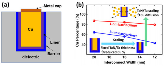
2.1. TaN Barrier/Liner Scaling
In order to maximize the Cu volume fraction, the TaN/Ta liner thickness must be reduced. In addition, the thickness of the Cu seed needs to be reduced to prevent the top pinch-off shape during subsequent Cu electroplating. However, the nonconformal step coverage of PVD results in gap-fill problems caused by the overhang and high resistance due to the thick barrier at the via bottom. Therefore, atomic layer deposition (ALD)/CVD is preferred for maximizing the gap-filling window and minimizing the resistance.
Several approaches have been explored for reducing the TaN barrier thickness. First, the minimum thickness can be reduced without sacrificing TaN barrier properties using PVD [9][45]. In particular, based on time-dependent dielectric breakdown (TDDB) measurements using a planar capacitor structure, TaN barrier characteristics have been shown to be retained even if the thickness is reduced to as low as 0.8 nm. In addition, it has been reported that using a Co/Ru liner instead of a Ta liner significantly improves the overall integrity of the TaN barrier [9][45]. However, due to the step coverage limit and the overhang problem associated with PVD, it is necessary to switch to ALD as the dimensions decrease. However, TaN thermally deposited using ALD has a higher number of impurities than PVD-fabricated TaN films, a lower film density, a higher resistance, and a lower interface quality, meaning that it cannot emulate the performance of PVD TaN at the same thickness. For this reason, PVD Ta and ALD TaN have been employed as bilayers (1 nm/1 nm) to reduce the thickness while ensuring the barrier properties [10][46]. Another approach is treating ALD-fabricated TaN in a PVD chamber to transform it into PVD-like film with optimal density and resistivity [11][12][47,48]. Using this method, the TaN thickness is 1.2 nm, compared with 1.5 nm for a Co liner and 2.0 nm for a Ru liner [12][48]. As a result, ALD has been combined with PVD to maintain the barrier properties and a low TaN thickness.
Scaling of the liner has also been actively carried out. The ALD/CVD method is required to overcome the step coverage and overhang problems, but a Ta liner cannot be used. Therefore, replacements for the Ta liner have been considered. Of these, Ru has received significant attention due to its suitability for ALD/CVD and the possibility of direct Cu plating without a PVD Cu seed layer [13][14][15][16][17][18][19][49,50,51,52,53,54,55]. In addition, Co has also been considered as a replacement for the Ta liner [20][56]. In [5][41], a Ru liner was found to be superior to a Co liner for Cu filling and electroplating with a liner thickness of 2 nm. However, the resistance of Ru was about 10% higher than that of Co as revealed by the temperature coefficient of resistance (TCR), which was believed to be due to interface and GB scattering. A Co liner has also been shown to outperform a Ru liner in terms of EM characteristics [21][57].
However, in order to fully exploit the excellent void-free gap-fill performance of Ru liners, approaches to improving their EM deficiencies have been reported. Co caps have been established as a standard process since the emergence of 14 nm technology. As a result, a significant improvement in EM performance has been observed with a Ru liner as the Co cap thickness increases [21][57]. It has also been demonstrated that the EM problem arises from the diffusion of Co from the cap to the liner due to the Co concentration gradient between the two [21][22][23][57,58,59]. Thus, a Co-doped Ru liner has been proposed to overcome this problem, and EM improvements have been reported [22][23][58,59]. Efforts to scale the TaN barrier and Co/Ru liner continue, but if the metal half-pitch decreases below 10 nm, the barrier/liner scaling limit is reached.
2.2. Selective Barrier Schemes
As advanced technologies emerge, the importance of the resistance and reliability of the vias increases. In particular, via resistance is strongly affected by the bottom thickness of the TaN. Therefore, as scaling progresses, the via resistance rapidly increases due to the thicker TaN. Furthermore, one of the most critical areas of a Cu-based DD structure is the bottom of the via, where the two metal levels meet [24][60], so selective deposition control of the via bottom barrier is advantageous for improved reliability. In this vein, argon (Ar) sputtering was used as a precleaning PVD barrier/liner [24][60]. The barrier-first process was conducted in the order of TaN/Ar sputtering/Ta instead of Ar sputtering/TaN/Ta to remove TaN in the via bottom and obtain a Cu/Ta/Cu interface. However, this process disappeared when the precleaning method for removing Cu oxide was changed from Ar sputtering to the oxide-reduction method.
Now that the via size is much smaller, self-assembled monolayers (SAM) have been pursued [25][26][61,62]. Figure 27 presents the process for the formation of a selective barrier on the via bottom. The Cu surface is passivated by depositing a SAM on the Cu surface subjected to the CuOx reduction treatment. The SAM should be highly selective and self-limited and be adsorbed onto metals but not other peripheral dielectrics. However, when the SAM attaches to the metal surface, it interferes with the adsorption of ALD TaN precursors, resulting in significant nucleation delays in ALD TaN growth [25][26][61,62]. As a result, ALD TaN does not deposit on the via bottom area where the SAM is located. The SAM is finally removed. The SAM process needs to be developed further before it can be adopted for mass production. Nevertheless, because it can achieve a reduction in the via resistance of about 50% and its TDDB and EM results are equivalent to the process of record (POR), it is likely to be useful in future advanced technologies [25][61].
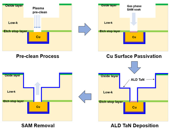
Figure 27. Selective barrier integration process. Reprinted/adapted with permission from Ref. [25]. 2021, IEEE.
Selective barrier integration process. Reprinted/adapted with permission from Ref. [61]. 2021, IEEE.
2.3. Self-Forming Barriers
Another promising approach to Cu extendibility is the through Co self-forming barrier (tCoSFB), a method in which manganese (Mn) atoms added to the seed Cu diffuse through the thin Co liner layer to form a strong diffusion barrier at the interface between the trench and the dielectric, as seen in Figure 38 [27][28][29][30][63,64,65,66].
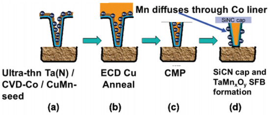
Figure 38. Through Co self-forming barrier (tCoSFB) structure and fabrication process. (a) an ultra-thin Ta(N)/CVD-Co film stack is formed on the patterned ULK pSiCOH surfaces, followed by a high-Mn% PVD-Cu(Mn) seed layer. (b) Cu electroplating and post-plating anneal. (c) CMP. (d) a PECVD SiCN(H) dielectric cap is deposited. Reprinted/adapted with permission from Ref. [27][63]. 2015, IEEE.
Initially, the Mn dopant is employed to form MnSixOy at the dielectric and Cu interface [28][29][31][32][64,65,67,68]. If CuMn seed deposition occurs without a barrier/liner and Cu plating and annealing are conducted, an SFB is created. This MnSixOy barrier is very thin and uniform, and its EM and TDDB performance is similar to that of POR. However, vertical trench triangular voltage sweep (VT-TVS) and O2 barrier tests indicate that MnSixOy is inadequate for blocking Cu and O2 diffusion, which led to the switch from the SFB to tCoSFB containing thin Ta(N) and Co [33][69].
The advantage of the tCoSFB process is that the cross-sectional area of Cu in the wiring can be maximized, and low line resistance can be obtained due to the 1 nm thickness of the Co liner and Ta barrier. However, because the line resistance and reliability balance are controlled by the Mn concentration of Cu(Mn) PVD, an increase in resistance may occur. Nevertheless, compared with the POR process, the results are encouraging, with improved resistance and EM and TDDB performance [30][34][66,70].
2.4. Hybrid Metallization
At the system-on-chip level, vias have become much more important for signal routing, and via resistance has increased significantly when downscaling the bottom contact area of the via. Therefore, introducing barrierless metal to the via is valuable, and metal−metal selective deposition is essential for the high-aspect-ratio (AR) vias. Hybrid metallization is a method of pre-filling a via with a barrierless metal and then filling the remaining metal area using Cu metallization, as seen in Figure 49 [35][71].
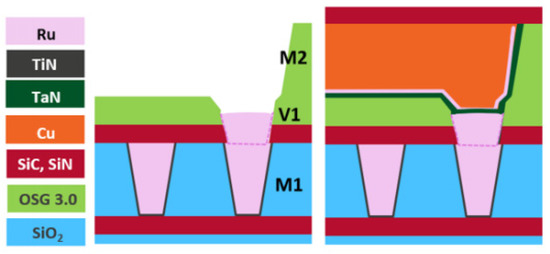
A barrierless prefill has a number of advantages. First, the prefill moves the barrier position of the Cu DD from the bottom to the top of the via, increasing the tapered via cross-section and reducing the resistance. Second, the gap–fill margin increases because SD trench metallization is employed. Third, because the high-AR vias are excluded, step coverage can be achieved with a thinner barrier/liner [36][72]. In addition, the optimized barrierless prefilling process may reduce RC delay by increasing the height of the vias and trenches, which can significantly improve circuit performance [37][73].
The first reported via prefill used Co [37][73]. However, due to Co ion drift, it was found that barrierless Co was not possible and that TiN barriers are required [36][38][72,74]. Ru has been found to be suitable for barrierless prefilling, resulting in a 40% reduction in via resistance and EM results that are similar to those for POR [35][71].
2.5. Alternative Metals
4.5. Alternative Metals
The thickness of the barrier layer cannot arbitrarily be reduced. If the thickness is less than a certain threshold, it no longer functions as a Cu diffusion barrier. Based on past experimental results, it is unclear whether the barrier/liner combination can have a thickness lower than 2 nm [9][10][11][39][45,46,47,75]. However, a barrierless solution is required when the half pitch falls below 10 nm, and thus, new metals to replace Cu have been sought. Some of these metals have a larger bulk resistivity than Cu but do not require a thick barrier/liner and exhibit lower resistance at sufficiently small dimensions because their inelastic average free path is shorter than that of Cu (39 nm) [40][41][76,77]. Examples of metals and substitutes proposed under these conditions include Ir, Rh, Mo [42][78], and W [43][79], but experimentally verified cases are rare except for Co and Ru [44][45][46][47][80,81,82,83].
Figure 510 displays the line resistance derived from the TCR according to the cross-sectional area of the conductor. Cu has a higher resistance than Ru and Co below ~400 nm2 at a 16-nm metal width and an AR of 2 [48][84].
2.6. Ru Semi-Damascene Schemes
4.6. Ru Semi-Damascene Schemes
Ru can be used in barrierless damascene structures and direct metal etching (DME). Figure 6 11 shows Ru metal implemented with subtractive etching.
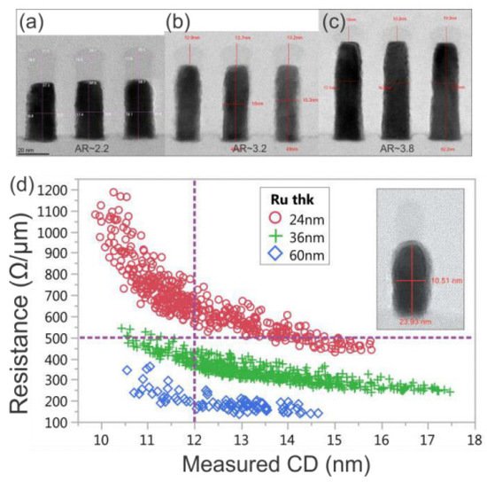
The use of subtractive etching opens up many possibilities that have not previously been possible for Cu damascene structures. First, because the Ru film is deposited on the entire wafer, the grain size is not limited by the damascene profile width. Therefore, it can significantly restrain the increase in resistance due to GB scattering. Second, the metal thickness is determined by Ru deposition, not by metal CMP. Therefore, if necessary, the resistance can be reduced by increasing the Ru thickness, and there is no AR-related filling problem. Third, because the metal thickness is not affected by the pattern density but is determined by the uniformity of the deposited Ru film, the variation in the metal Rs will be reduced. Finally, a space between Ru metal with an increase in the AR could be introduced by employing an intentional air gap.
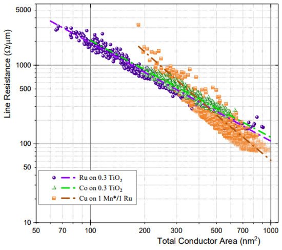
The semi-damascene process is an interesting approach that utilizes the advantages of Ru, such as barrierless designs and subtractive etching. This method begins with vias fabricated in a low-k material, and the vias and trench layers are filled using a single deposition step. Subtractive etching is then applied to the trench patterning [49][50][51][52][14,85,86,87]. According to the latest result, Ru line resistance outperforms Cu at 270 nm2 or lower (CD < 12 nm) based on line resistance vs. conducting area plot, and the EM and TDDB results are promising so far [53][17]. For this reason, the Ru semi-damascene process is the most competitive candidate for use in 3 nm technology and lower.
Figure 712 shows the conceptual summary of the metallization approaches mentioned in this section as they have evolved. As shown in the figure, the main trend of metallization has been to reduce the area ratio occupied by the barrier in the scaled wire. Traditional attempts were to reduce the existing barrier/liner (TaN/Ta) thickness by replacing a new process method (ALD) and a new liner material (Co/Ru). After that, it was gradually developed to implement a barrier-free process using Co or Ru. Moreover, the boundary has recently been extended to the subtraction etch process using Ru instead of the Cu damascene scheme.
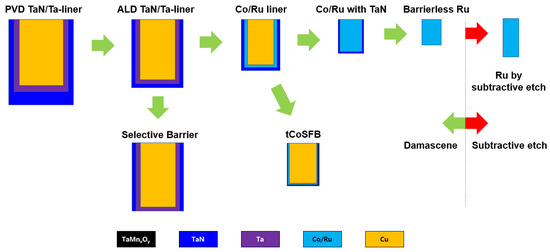
Figure 712. Trends in recent metallization approaches.
In addition to the metallization approaches mentioned here, various studies are being conducted. One of them is the study of a 2D-like barrier. The approach is to minimize the volume fraction of Cu occupied by the barrier by replacing the thick Ta or TaN barrier with 2D-like materials such as graphene [54][55][88,89], MoS2 [5][56][41,90], TaS2 [5][41], and WSe2 [5][41].