Several kinds of chemical vapor deposition (CVD) methods have been extensively used in the semiconductor industries for bulk crystal growth, thin film deposition, and nanomaterials synthesis. The MW-SWP CVD system consisting of a waveguide, slot antenna, and dielectric windows is significant for generating high -density plasma with low electron temperature, enabling low -temperature growth of materials without damaging the surface of base substrates. The synthesis of graphene and hexagonal boron nitride (hBN) films has been achieved on metals, semiconductors, insulators, and dielectric substrates for application in photovoltaics, sensors, batteries, supercapacitors, fuel cells, and various other electronic devices.
- surface wave plasma
- chemical vapor deposition
- graphene
1. Introduction
The discovery of graphene, an atomically thin sheet of sp2 hybridized carbon atoms has revolutionized the field of research oin physics, chemistry, materials science, and engineering [1][2][3]. The band structure of two-dimensional (2D) graphene lattice is unique in comparison to all other bulk semiconductor materials, as the massless Dirac fermions in graphene moves at ballistic speed in submicron length, close to relativistic speeds [4][5][6]. The exceptional electrical properties of graphene have triggered significant interest for application in next -generation electronic devices [7][8][9][10]. Furthermore, several studies have demonstrated the unique optical, mechanical, thermal, and chemical properties ofor 2D graphene sheets, which are significant to develop advanced material systems for a wide range of applications [11][12][13][14]. Subsequently, various other 2D materials were discovered considering the similar layered structured materials, most notably, insulating hexagonal boron nitride (hBN) layers and semiconducting transition metal dichalcogenide (TMDCs) layers [15][16][17][18]. All of these discoveries have opened a new frontier in material science to take the advances of diverse properties of 2D materials. This has also enabled the realization of other new classes of 2D layered materials, such as heteroatom incorporated layers, twisted layered structures, and atomically thin heterostructures [19][20][21][22].
Most of the intrinsic properties of 2D layered materials have been explored by mechanical exfoliation from bulk crystals, which is becoming a unique technology for 2D material systems. Mechanically exfoliated 2D materials have also been explored to fabricate the assembly of twisted layers and heterostructures [23][24][25]. In another aspect, a graphene oxide layer, dichalcogenide layers, metal oxide layers, and MXenes were chemically exfoliated for application as functional materials in energy storage and conversion devices [26][27][28]. The mechanical exfoliation of 2D materials is significant to fabricate electronic devices preserving the intrinsic properties, whereas chemical exfoliation is a versatile technique to derive 2D materials in large quantityies for energy storage/conversion device applications. In contrast to the exfoliation process, the growth of 2D materials on a suitable substrate with control growth orientation can be significant for device applications [29][30][31][32]. In a growth technique, synthesis of 2D layered materials can be achieved with control layer numbers, shape, and size of single crystals [33][34][35][36]. Furthermore, edge structures, vacancies, heteroatoms doping, and adatoms incorporation can be controlled in the 2D crystals in a growth technique, thereby controlling or introducing new functionalities [37][38][39][40]. Among several growth techniques, the chemical vapor deposition (CVD) method has been widely accepted for the growth of 2D materials. The thermal CVD process is one of the simplest techniques for the growth of graphene, hBN, and TMDCs layered materials, using various kinds of precursors materials [41][42][43][44]. The main drawback of the thermal CVD process is the requirement of high temperature (>1000 °C) and catalytic substrates for the synthesis of graphene and hBN. In contrast to the thermal CVD process, it has been demonstrated that a plasma CVD method can be more effective for the growth of graphene-based materials at a lower temperature on both the catalytic orand noncatalytic substrates [45][46][47][48]. Synthesis of graphene, hBN, and TMDCs -based 2D materials has been demonstrated by the plasma CVD method [49][50][51]. Table 1 presents a comparison of plasma CVD and various other growth techniques for the growth of graphene and related 2D layered materials [52][53][54][55][56].| Methods | Graphene | Hexagonal Boron Nitride (hBN) | Transition Metal Dichalcogenides (TMDCs) Layers | |||
|---|---|---|---|---|---|---|
| Pulsed-Laser Deposition (PLD) | Monolayer/Bilayer/Fewlayers (Catalytic growth; Temperature: 300~1200 °C) | Monolayer/Fewlayers (Catalytic & noncatalytic growth; Temperature: 200~1000 °C) | Fewlayers/Multilayers (Noncatalytic growth; Temperature: 300~800 °C) | |||
| Magnetron Sputtering | Monolayer/Fewlayers(Catalytic growth; Temperature: 300~1000 °C) | Fewlayers/Multilayers (Catalytic growth & noncatalytic growth; Temperature: 400~1000 °C) | Monolayer/Fewlayers (Noncatalytic growth; Temperature: 300~800 °C) | |||
| Molecular Beam Epitaxy (MBE) | Monolayer/Bilayer/Fewlayers (Catalytic growth; Temperature: 500~1000 °C) | Monolayer/Bilayer/Fewlayers (Catalytic growth; Temperature: 400~1000 °C) | Monolayer/Fewlayers (Noncatalytic growth; Temperature: 600~1000 °C) | |||
| Thermal Chemical Vapor Deposition (CVD) | Monolayer/Bilayer/Fewlayers (Catalytic growth; Temperature: >1000 °C) | Monolayer/Bilayer/Fewlayers (Catalytic growth; Temperature: >1000 °C) | Monolayer/Bilayer/Fewlayers (Noncatalytic growth; Temperature: 600~1000 °C) | |||
| Plasma Chemical Vapor Deposition (CVD) | Monolayer/Bilayer/Fewlayers (Catalytic & noncatalytic growth; Low temperature growth) | Monolayer/Bilayer/Fewlayers (Catalytic & noncatalytic growth; Low-temperature growth) | Monolayer/Fewlayers/Multilayers (Catalytic & noncatalytic growth; Low temperature growth) | Monolayer/Fewlayers/Multilayers (Catalytic & noncatalytic growth; Low-temperature growth) | Monolayer/Fewlayers/Multilayers (Noncatalytic growth; Low temperature growth) | Monolayer/Fewlayers/Multilayers (Noncatalytic growth; Low-temperature growth) |
Among various plasma CVD processes, the microwave-excited surface wave plasma CVD (MW-SWP CVD) process is an exceptional technique to synthesize graphene and other related 2D materials [57][58][59][60].
2. Growth of Graphene and 2D Materials
Growth of graphene by the plasma CVD process can be achieved on various substrates, such as metals, insulators, and semiconductors, at a significantly lower temperature than the thermal CVD process [61][62][63][64]. Moreover, the synthesis of 2D materials, such as hBN, has been achieved by the plasma CVD technique [65]. Synthesis of graphene and hBN films hasve mostly been investigated on transition metal catalysts (such as Cu, Ni, Mo, etc.) or their alloy substrates (e.g., NiCu, NiMo, CuSn, etc.) in a CVD process [36][37][38][66]. The graphene synthesis on Cu substrate is significantly investigated due to their low carbon solubility and surface -mediated catalytic growth of graphene layers. In another prospect, graphene films can be directly grown on a noncatalytic substrate by the plasma CVD techniques, considering the decomposition of precursor gas molecules in the plasma and forming plasma radicals for graphene growth at a considerably lower temperature [67].
2.1. Growth of Graphene Films on Catalytic Substrates
Synthesis of a monolayer graphene film by the microwave plasma CVD (MWP CVD) process has been demonstrated on Ni foil at a temperature of 450 °C [68]. Subsequently, graphene synthesis by the MW-SWP CVD technique was developed, considering the advantage of large-scale growth at a significantly lower temperature (300–400 °C) [69]. Synthesis of a few-layer graphene film on the Cu foil was achieved by the developed MW-SWP CVD process. The graphene film with excellent transparency and electrical conductivity is demonstrated for transparent electrode applications, which can be used in optoelectronics and nanoelectronics devices. The synthesized graphene on Cu and Al foil by the MW-SWP CVD process was analyzed by Raman spectroscopy. It was obtained that the synthesized graphene films were of few-layer structures. The intensity of the 2D peak is significantly higher than the G peak, which significantly differs from the monolayer graphene synthesized by the thermal CVD process. Similarly, Raman analysis confirms graphene film growth on the Al foil by the MW-SWP CVD technique. The spatial distribution of sheet resistance for the transferred graphene film was analyzed, which was found to be in the range of 1.0 to 4.1 kΩ/Sq over the area of 23 × 20 cm2 [69].
Synthesis of graphene films by a similar MW-SWP CVD system was demonstrated by the group using gaseous and solid precursors at a lower substrate temperature [70][71][72]. Graphene growth was achieved on Cu foil without any pretreatment at a gas composition pressure of 45 Pa, a microwave power of 1.2 kW, and a growth duration of 2–4 min. Figure 1a shows the Raman spectra of the graphene films deposited at a substrate temperature of 400 and 500 °C. Further, Figure 1b shows the Raman spectra at a substrate temperature of 240, 270, and 300 °C, indicating the presence of a 2D peak and the formation of a few- layers of graphene film. As presented in the figure, a disorder-induced D band is observed at approximately 1348 cm−1, indicating phonon scattering at defect sites and impurities. An intense graphitic G band is also observed at approximately 1574 cm−1, attributinged to the sp2 phonon vibrations. Three other peaks were observed at approximately 2685, 2914, and 3210 cm−1, corresponding to 2D, G + D, and 2G second-order Raman spectra, respectively. The presence of a 2D and a 2G peak indicates good agreement of the graphene structure formation in the carbon film. The Raman characteristic for the graphene film deposited at 400 and 500 °C is almost identical, having a similar G and 2D peak intensity. The D and D + G peaks presented defect -related structures in the sp2 hybridized graphene film [70].
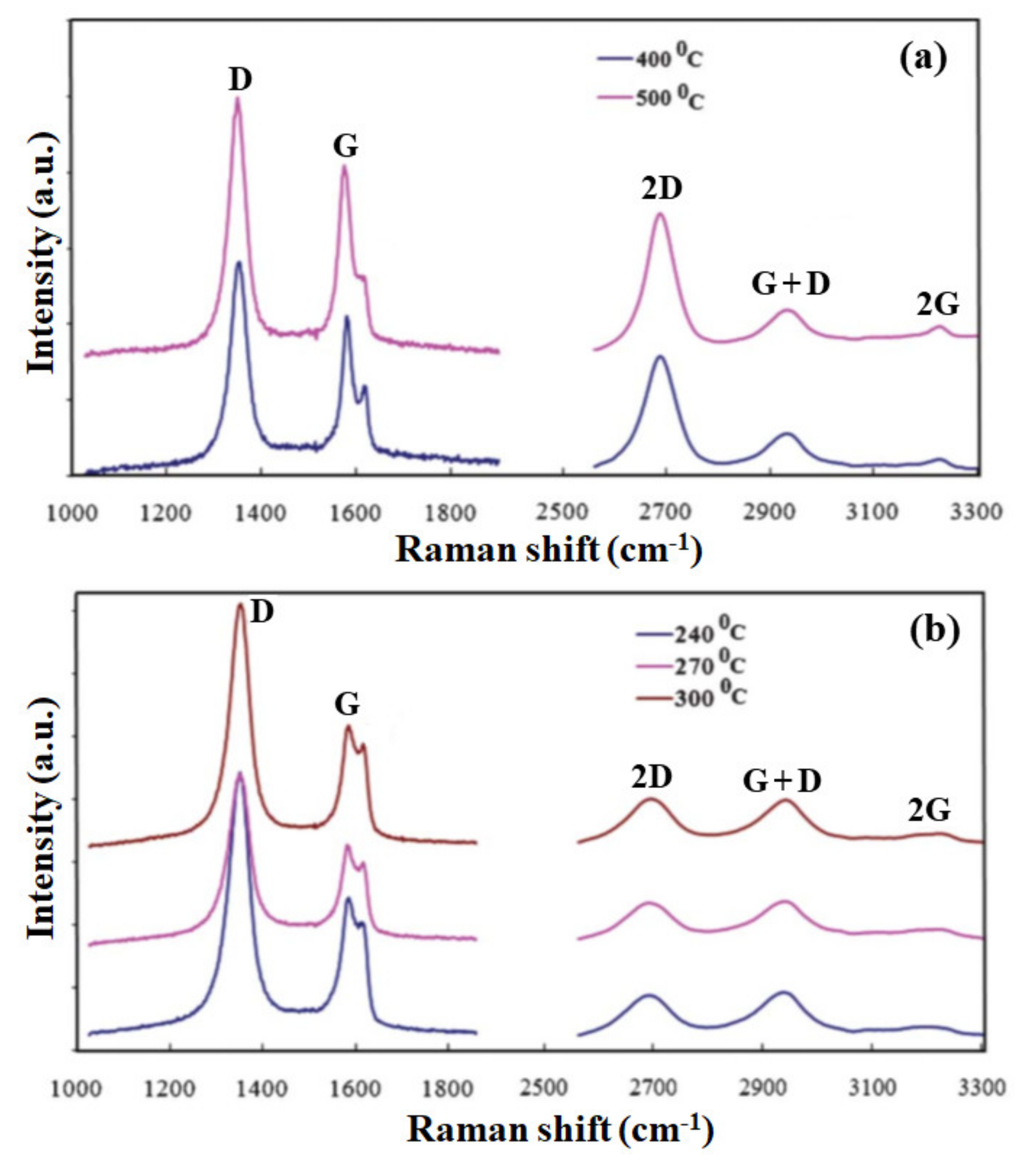
Figure 1. Raman spectra of the graphene film deposited on Cu foil at low temperature by the MW-SWP CVD method. Raman spectra of a graphene film at (a) lower and higher Raman shifts, deposited at a substrate temperature of 400 and 500 °C. (b) Raman spectra of a graphene film at lower and higher Raman shifts, deposited at a substrate temperature of 240, 270, and 300 °C, indicating the presence of a 2D peak and formation of a few- layers of graphene.
The synthesized graphene films were analyzed by XPS and SEM to determine the chemical and the morphological structures. Figure 2a,b shows the wide XPS spectra and C1s spectra for different substrate temperatures. The XPS analysis shows a small oxygen (O1s) peak along with the dominant C1s peak. No other difference in chemical composition was observed for all the graphene samples. Figure 2c shows the SEM images of the as-synthesized graphene film on Cu foil at 240 °C, presenting graphene grain and Cu steps. Figure 2d shows the SEM image of transferred graphene film on a plastic substrate presenting wrinkle formation, which is a common feature ofor the transferred graphene film [70].
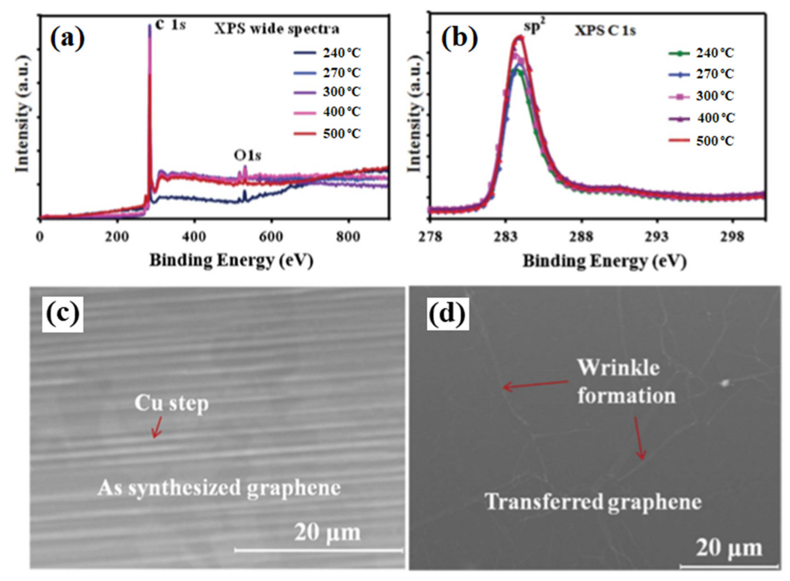
Figure 2. XPS analysis of the synthesized graphene film on Cu foil by the MW-SWP CVD method. (a) A wWide XPS spectra and (b) C1s XPS spectra at different substrate temperatures. SEM images of (c) as grown graphene film on Cu foil at 240 °C and (d) transferred graphene film on a plastic substrate presenting wrinkle formation.
Figure 3 shows the schematic presentation of the MW-SWP CVD method for graphene synthesis using camphor as a solid precursor [71]. In this approach, solid camphor powder was directly inserted in the MW-SWP CVD chamber as a carbon precursor. The camphor powder is easily evaporated inside the CVD chamber and diluted with Ar gas to generate plasma. Figure 3a shows the Raman spectra of the synthesized graphene films on Cu foil at temperatures of 500 and 560 °C. Figure 3b shows the optical microscope image of graphene film transferred on a plastic substrate. A continuous film with high transparency and conductivity was obtained on the plastic substrate. Figure 3c shows the SEM image of the as-synthesized graphene film on the Cu foil, where domain -like structures of the graphene film can be observed. Figure 3d shows the SEM image of the transferred graphene film. The formation of wrinkles in the graphene film can be observed from the SEM analysis. The formation of such wrinkles in the transferred graphene film is consistent for the MW-SWP CVD synthesized samples, which is also the case for other CVD synthesized transferred graphene films [71]. Further, PMMA has been used as a precursor coated on Cu foil for graphene synthesis by the MW-SWP CVD method. FThe formation of graphene was confirmed at a substrate temperature as low as 280 °C. The Raman peak obtained onat various positions of the sample was almost similar considering the uniform growth of the few-layer graphene with homogenous distribution of plasma [72]. Synthesis of the bilayer graphene using PMMA and CH4 as precursors has been demonstrated by the MW-SWP CVD at a significantly lower temperature. It has been observed that a carrier mobility of 740 cm2 V−1 s−1 can be obtained for the bilayer graphene synthesized by the MW-SWP CVD method [73]. Ichimura et al. have demonstrated obtaining maximum Hall mobility of approximately 625 cm2 V−1 s−1 for the synthesized thin graphitic film by the MW-SWP CVD method [74]. Further, Hall mobility of approximately 398 cm2 V−1 s−1 has been obtained for a carbon dot -doped graphene film synthesized by the MW-SWP CVD method [75]. It has been obtained that low carbon precursor concentration can be ideal for controlling the graphene domain growth with particular layer numbers. Although few-layer graphene film can be synthesized on the metal catalytic substrate by the MW-SWP CVD method at a significantly lower substrate temperature, control growth of monolayer graphene still remains a significant challenge. These studies gave a detailed overview of graphene synthesis by the MW-SWP CVD process for graphene growth on a catalytic metal substrate using the gaseous, solid, and other precursors. The graphene growth in the MW-SWP CVD technique can be further investigated for control layer growth with larger grain size on metal catalytic substrates. In this prospect, ethe effect of plasma interaction with the substrate surface can be critical, where the plasma radicals play a dominant role in graphene nucleation and growth.
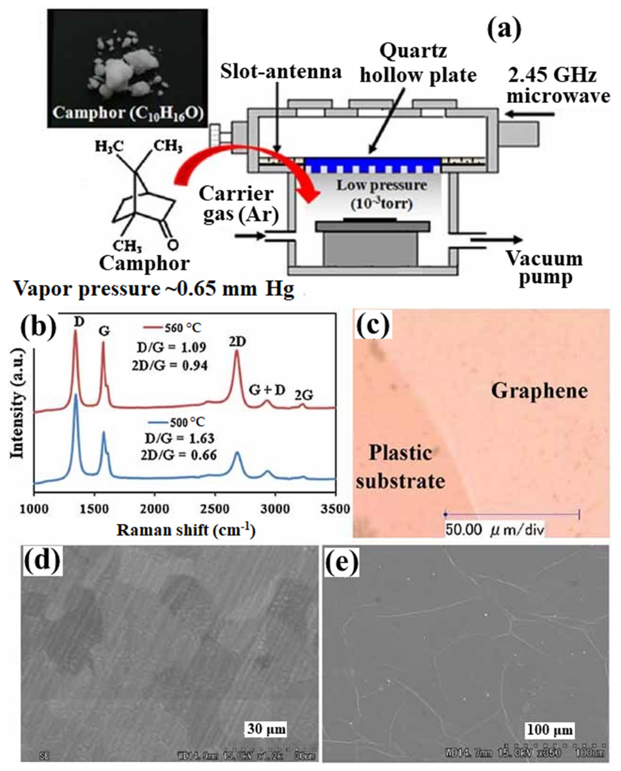
Figure 3. (a) Schematic presentation of the MW-SWP CVD method for graphene synthesis using camphor as a solid precursor. (b) Raman spectra of the synthesized graphene films on Cu foil at temperatures 500 and 560 °C. (c) Optical microscope image of graphene film transferred on a plastic substrate. SEM image of (d) as-synthesized and (e) transferred graphene films.
2.2. Direct Growth of Graphene on Arbitrary Substrates
Synthesis of graphene film directly on semiconducting, insulating, and dielectric substrates by the plasma CVD process is of great interest to avoid the transfer process and enablinge direct integration in electronic devices. Synthesis of the graphene film on an arbitrary substrate by the MW-SWP CVD technique was demonstrated by the group [76]. The graphene film was synthesized using a gas mixture of C2H2 and Ar with a gas composition pressure of 45 Pa and for a growth duration of 70–120 s. Figure 4 shows the Raman spectra of graphene films deposited on glass and silicon substrates at 400, 500, and 560 °C by the developed MW-SWP CVD method. Figure 4a shows the Raman studies of the carbon films deposited on glass substrates at different temperatures. The Raman spectra showed a strong and sharp graphitic G band at approximately 1568 cm−1, representing the crystalline sp2 hybridized carbon atoms for the nanographene domains. A disorder-induced D band is observed at 1339 cm−1; the high intensity of the D peak originates from either the small crystallite sizes or an abundance of edges in the nanographene structures. Three other peaks are observed at 2669, 2915, and 3214 cm−1, corresponding to 2D, G + D, and 2G second-order Raman peaks. The presence of a distinct 2D peak confirmed the presence of a graphene structure in the synthesized carbon films. Similarly, Figure 4b shows the Raman studies of the carbon films deposited on silicon substrates, presenting the D, G, and 2D peaks at approximately 1341, 1566, and 2665 cm−1, respectively. The Raman studies showed that the structure of the nanographene film is similar and independent of the Si or SiO2 substrates. The graphene film deposited at 560 °C showed a greatly enhanced 2D peak, and a more suppressed D + G peak compared to those of the low temperature deposited films, indicating a more ordered graphene structure. These studies presented that the CVD process can be used for direct deposition of nanographene films on different substrates without using a metal catalytic layer. The deposition of a graphene film on a noncatalytic substrates is due to the formation of carbon radicals with hydrogen termination in the microwave plasma, which plays a key role in the nucleation and growth process on the metal-free substrate surfaces. The carbon radicals of the plasma absorb onto the substrate surface and bonds to other such radicals by a diffusion process to form sp2 carbon [76].
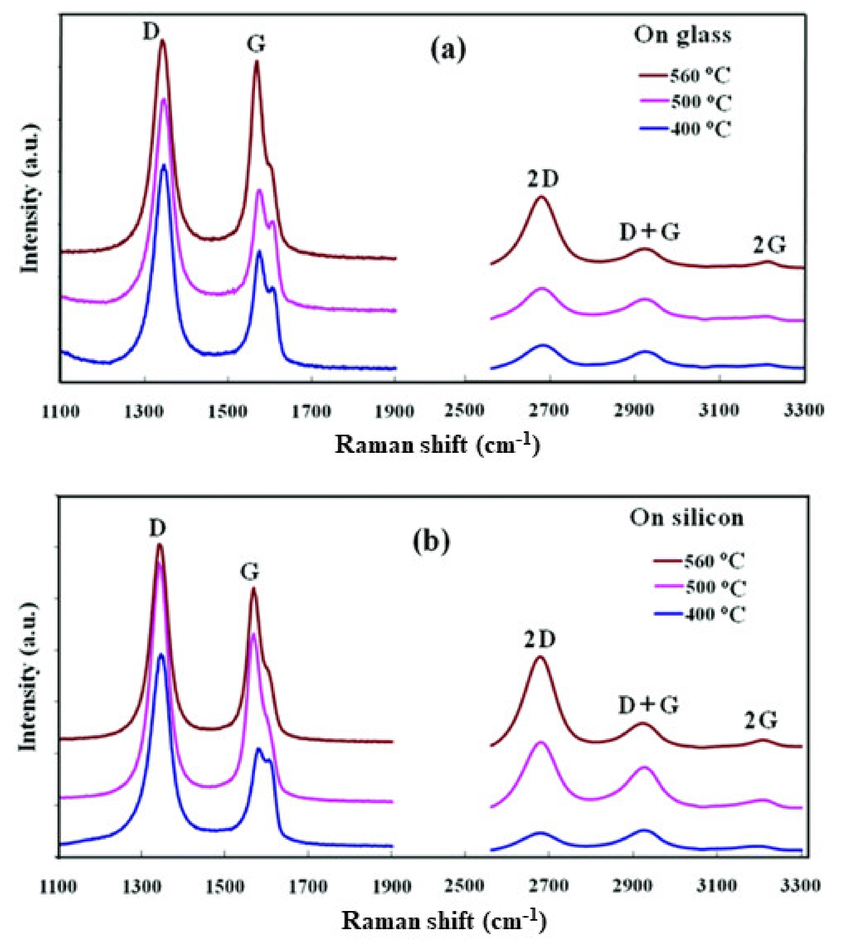
Figure 4. Raman spectra of graphene film deposited on glass and silicon substrates by the developed MW-SWP CVD method. Raman spectra of the nanographene films were deposited at 400, 500, and 560 °C on (a) glass and (b) n-silicon substrates.
The synthesized graphene films were characterized by transmittance and electrical conductivity analysis. The graphene films were highly transparent to visible light as it was synthesized for a very short duration. Figure 5a shows the transmittance of the nanographene films deposited at 560 °C for different durations in comparisoned to indium tin oxide (the inset of the figure shows a photograph of nanographene film deposited on the SiO2 substrate). The transmittance of the graphene film deposited for the shortest duration was 82% at a wavelength of 550 nm. Figure 5b shows the J-V characteristics of the fabricated devices with nanographene films deposited for different durations. As the thickness of the deposited graphene film increased with an increase in growth time, the conductivity of the graphene film increased. The graphene films obtained on the glass and silicon substrates can be significant for various device applications. Further, the developed process paves the way to deposit graphene film on an arbitrary substrate depending on the application in optoelectronic and nanoelectronic devices. In the following, researchers discuss the fabrication of a graphene/silicon Schottky junction solar cell for a deposited nanographene film directly on a silicon substrate. A photovoltaic device was configured with the directly grown nanographene film on the n-silicon substrate. Figure 5c shows a schematic diagram of the fabricated nanographene/n-silicon heterojunction device. The incident light in the device can transmit through the transparent graphene film and be absorbed in the n-silicon to generate photo-exciton. Figure 5d shows an energy band diagram of the nanographene/n-silicon photovoltaic device in thermal equilibrium. Due to the metallic nature of the graphene film, a Schottky junction can be formed with the n-silicon substrate. Several studies have shown that a thermal CVD synthesized graphene film can be transferred on the silicon substrate to form a Schottky junction device, creating a large built-in field (Vbi, 0.55–0.75 V) [77]. Due to the presence of a large built-in field in the graphene/n-silicon junction, there can be efficient charge separation and transportation. Figure 5e shows a log scale plot for the dark J-V characteristics of the fabricated nanographene/n-silicon device. A device ideality factor of 2.44 was calculated from the J-V log plot as in the inset of Figure 5e. The fabricated device was characterized under the illumination of white light with an intensity of 100 mW/cm2. Figure 5f shows the J-V characteristics of the graphene/silicon Schottky junction, presenting a photovoltaic action with a conversion efficiency of 2.1%. Recently, it has been demonstrated that a solar cell conversion efficiency can be achieved by more than 6% for the directly grown graphene film by the MW-SWP CVD on silicon substrate [78]. Further, the synthesis of graphene on catalytic/noncatalytic substrates has been investigated using LASER irradiation on the substrate surface in the MW-SWP CVD method. It has been observed that graphene growth can be achieved under LASER irradiation, whereas graphene growth was not observed only with the plasma process for the particular growth conditions [79]. These studies are significant for the direct growth of graphene structures on noncatalytic semiconducting, insulating, and dielectric substrates for potential applications in optoelectronic, sensor, solar cells, and heterojunction devices. Further, the synthesis of graphene with control growth orientation can be a significant aspect to utilize the graphene surface for application in energy storage and conversation devices.
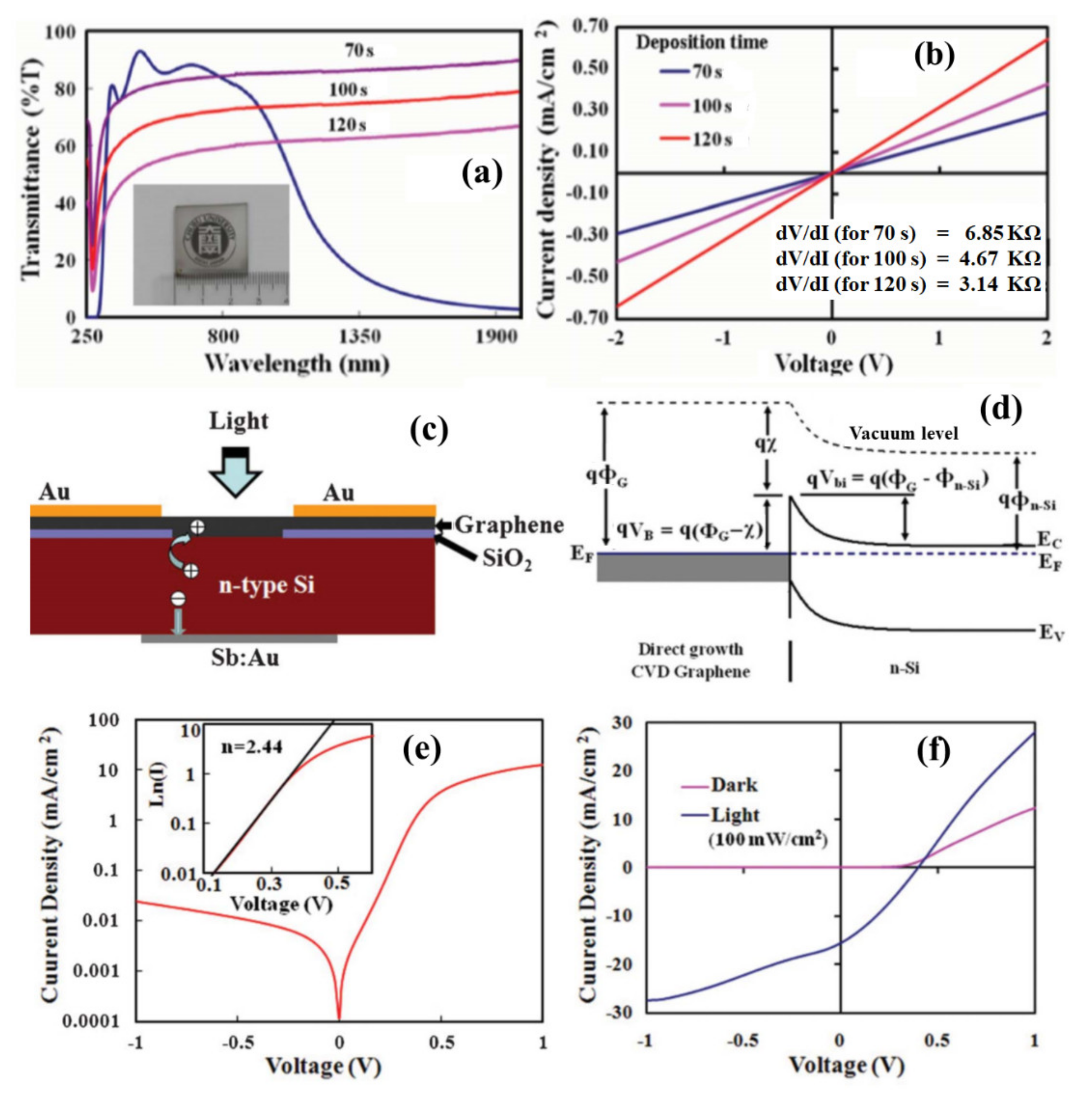
Figure 5. (a) The transmittance of the nanographene films deposited at 560 °C for different durations in comparisoned to indium tin oxide coated glass (inset of the figure: a photograph of nanographene film deposited on glass). (b) J-V characteristics of the fabricated devices with nanographene films deposited for different durations. (c) Schematic diagram of fabricated graphene/n-silicon Schottky junction device. (d) Energy-band diagram of the fabricated device. (e) J-V curve as a log plot under dark conditions (inset fitting plot of ln(I)-V in forward bias). (f) J-V characteristics for the dark and light irradiation (100 mW/cm2) conditions.
3. Future Prospects of MW-SWP CVD for 2D Materials Synthesis
The MW-SWP CVD method has been successfully established as a versatile CVD technique to grow graphene film on metals, semiconductors, insulators, and dielectric substrates independent of their catalytic and noncatalytic properties. However, controlling the crystalline quality and layer numbers for the synthesized graphene film is a significant challenge for the developed MW-SWP CVD method. Again, the electrical properties of the graphene film deposited by the plasma CVD method is not as good as the thermal CVD method as discussed above due to higher defects and smaller grain sizes, nevertheless, application in various electronic devices can be explored considering the possibility of direct growth and thereby overcoming the influence of interface trap states due to impurities. Furthermore, controlling the vertically-aligned graphene sheet synthesis process can be significant, where the spacing of graphene sheets, length, and adhesibility with substrate surface are key aspects for various prospective applications. The MW-SWP CVD method has been used to synthesize wafer-scale hBN film on the catalytic and noncatalytic substrates. The thickness of hBN film can be controlled and a much thicker film can be synthesized in on a wafer scale compared to the thermal CVD process, as the monolayer and the few-layer hBN growth are limited by the catalytic growth nature of the substrate in a thermal CVD process. Further, graphene-like BCN structures and other 2D layered materials can be synthesized by the developed process as a gaseous and solid precursor can be introduced in the growth chamber. Synthesis of graphene/hBN heterostructures and other heterostructures of 2D layered materials can be interesting prospects for future studies in MW-SWP CVD methods. Sulfurization of metal films and use of metal -organic precursors can be interesting prospects for low -temperature synthesis of TMDCs layers by the MW-SWP CVD method. The MW-SWP can be also an important technique for processing of graphene oxide, MXenes, oxide layered materials, and other nanomaterials. Recently, researchers demonstrated the near-room temperature reduction of graphene oxide films and doping of nitrogen atoms [49]. Interestingly, graphene oxide films coated on the flexible polymer substrates can be processed by MW-SWP, opening possibilities for the reduction and incorporation of doping elements in graphene oxide films on various soft substrates. In other prospects, the MW-SWP process can be used for functionalizing, surface processing, encapsulation, and incorporation of doping elements, thereby expanding the application of plasma methods.
References
- Novoselov, K.S.; Geim, A.K.; Morozov, S.V.; Jiang, D.; Zhang, Y.; Dubonos, S.V.; Grigorieva, I.V.; Firsov, A.A. Electric field effect in atomically thin carbon films. Science 2004, 306, 666-669.
- Zhang, Y.; Tan, Y.W.; Stormer, H.L.; Kim, P. Experimental observation of the quantum Hall effect and Berry’s phase in graphene. Nature 2005, 438, 201-204.
- Geim, A.K.; Novoselov, K.S. The rise of graphene. Nat. Mater. 2009, 6, 183–191.
- Castro Neto, A.H.; Guinea, F.; Peres, N.M.R.; Novoselov, K.S.; Geim, A.K. The electronic properties of graphene. Rev. Mod. Phys. 2009, 81, 109-162.
- Du, X.; Skachko, I.; Andrei, E.Y.; Barker, A. Approaching ballistic transport in suspended graphene. Nat. Nanotechnol. 2008, 3, 491-495.
- Lin, Y.M.; Dimitrakopoulos, C.; Jenkins, K.A.; Farmer, D.B.; Chiu, H.Y.; Grill, A.; Avouris, P. 100-GHz transistors from wafer-scale epitaxial graphene. Science 2010, 327, 662.
- Eda, G.; Fanchini, G.; Chhowalla, M.; Large-area ultrathin films of reduced graphene oxide as a transparent and flexible electronic material. Nat. Nanotechnol. 2008, 3, 270-274.
- Schedin, F.; Geim, A.K.; Morozov, S.V.; Hill, E.W.; Blake, P.; Katsnelson, M.I.; Novoselov, K.S. Detection of individual gas molecules adsorbed on graphene. Nat. Mater. 2007, 6, 652-655.
- Raccichini, R.; Varzi, A.; Passerini, S.; Scrosati, B. The role of graphene for electrochemical energy storage. Nat. Mater. 2015, 14, 271-279.
- Bae, S.; Kim, H.; Lee, Y.; Xu, X.; Park, J.-S.; Zheng, Y.; Balakrishnan, J.; Lei, T. Kim, H.R.; Song, Y.; et al. Roll-to-roll production of 30-inch graphene films for transparent electrodes. Nat. Nanotechnol. 2010, 5, 574-578.
- Vineesh, T. V.; Kumar, M. P.; Takahashi, C.; Kalita, G.; Alwarappan, S.; Pattanayak, D. K.; Narayanan, T. N. Bifunctional electrocatalytic activity of boron‐doped graphene derived from boron carbide. Adv. Energ. Mater. 2015, 5, 17, 1500658.
- Balandin, A.A.; Ghosh, S.; Bao, W.; Calizo, I.; Teweldebrhan, D.; Miao, F.; Lau, C.N. Superior thermal conductivity of single-layer graphene. Nano Lett. 2008, 8, 902-907.
- Nair, R.R.; Blake, P.; Grigorenko, A.N.; Novoselov, K.S.; Booth, T.J.; Stauber, T.; Peres, N.M.R.; Geim, A.K. Fine structure constant defines visual transparency of graphene. Science 2008, 320, 1308.
- Heersche, H. B.; Jarillo-Herrero, P.; Oostinga, J. B.; Vandersypen, L. M. K.; Morpurgo, A. F. Bipolar supercurrent in graphene. Nature 2007, 446, 56.
- Mak, K.F.; Lee, C.; Hone, J.; Shan, J.; Heinz, T.F. Atomically thin MoS₂: A new direct-gap semiconductor. Phys. Rev. Lett. 2010, 105, 136805.
- Desai, P.; Ranade, A.K.; Mahyavanshi, R.; Tanemura, M.; Kalita, G. Influence of MoS2-silicon interface states on spectral photoresponse characteristics. Phys. Status Solidi A 2019, 216, 18, 1900349.
- Mahyavanshi, R.D.; Kalita, G.; Sharma, K.P.; Kondo, M.; Dewa, T.; Kawahara, T.; Tanemura, M. Synthesis of MoS2 ribbons and their branched structures by chemical vapor deposition in sulfur-enriched environment. Appl. Surf. Sci. 2017, 409, 396-402.
- Thangaraja, A.; Shinde, S.M.; Kalita, G.; Tanemura, M. An effective approach to synthesize monolayer tungsten disulphide crystals using tungsten halide precursor. Appl. Phys. Lett. 2016, 108, 053104.
- Wang, X.; Meng, L.; Li, B.; Gong, Y. Heteroatom doped graphene engineering for energy storage and conversion. Mater. Today 2021, 47, 108-130.
- Zhua, H.; Gan, X.; McCreary, A.; Lv, R.; Lin, Z.; Terrones, M. Heteroatom doping of two-dimensional materials. Nano Today 2020, 30, 100829.
- Liu, X.; Zhang, N.J.; Watanabe, K.; Taniguchi, T.; Li, J.I.A. Isospin order in superconducting magic-angle twisted trilayer graphene. Nat. Phys. 2022, 18, 522-527.
- Mahyavanshi, R.D.; Kalita, G.; Ranade, A.; Desai, P.; Kondo, M.; Dewa, T.; Tanemura, M. Photovoltaic action with broadband photoresponsivity in germanium-MoS2 ultrathin heterojunction. IEEE Trans. Electron. Devices 2018, 65, 4434-4440.
- Zhang, Y.; Tang, T.T.; Girit, C.; Hao, Z.; Martin, M.C.; Zettl, A.; Crommie, M.F.; Shen, Y.R.; Wang, F. Direct observation of a widely tunable bandgap in bilayer graphene. Nature 2009, 459, 820-823.
- Rickhaus, P.; Zheng, G.; Lado, J.L.; Lee, Y.; Kurzmann, A.; Eich, M.; Pisoni, R.; Tong, C.; Garreis, R.; Gold, C.; et al. Gap opening in twisted double bilayer graphene by crystal fields. Nano Lett. 2019, 19, 8821-8828.
- Mills, S.; Mizuno, N.; Wang, P.; Lyu, J.; Watanabe, K.; Taniguchi, T.; Camino, F.; Zhang, L.; Du, X. Contact transparency in mechanically assembled 2D material devices. J. Phys. Mater. 2019, 2, 035003.
- Kalita, G.; Sharma, S.; Wakita, K.; Umeno, M.; Hayashi, Y.; Tanemura, M. A photoinduced charge transfer composite of graphene oxide and ferrocene. Phys. Chem. Chem. Phys. 2013, 15, 1271-1274.
- Shinde, S. M.; Kalita, G.; Tanemura, M. Fabrication of poly(methyl methacrylate)-MoS2/graphene heterostructure for memory device application. J. Appl. Phys. 2014, 116(21), 214306
- Radisavljevic, B.; Radenovic, A.; Brivio, J.; Giacometti, V.; Kis, A. Single-layer MoS2 transistors. Nature Nanotech. 2011, 6, 147-150.
- Gogotsi, Y.; Anasori, B. The rise of MXenes. ACS Nano 2019, 13, 8, 8491-8494.
- Yu, Q.; Lian, J.; Siriponglert, S.; Li, H.; Chen, Y.P.; Pei, S.-S. Graphene segregated on Ni surfaces and transferred to insulators. Appl. Phys. Lett. 2008, 93, 113103.
- Kalita, G.; Masahiro, M.; Uchida, H.; Wakita, K.; Umeno, M. Few layers of graphene as transparent electrode from botanical derivative camphor. Mater. Lett. 2010, 64, 2180-2183.
- Kim, K.S.; Zhao, Y.; Jang, H.; Lee, S.Y.; Kim, J.M.; Kim, K.S.; Ahn, J.; Kim, H.P.; Choi, J.Y.; Hong, B.H. Large-scale pattern growth of graphene films for stretchable transparent electrodes. Nature 2009, 457, 706-710.
- Li, X.S.; Cai, W.W.; An, J.H.; Kim, S.; Nah, J.; Yang, D.X.; Piner, R.; Velamakanni, A.; Jung, I.; Tutuc, E.; et al. Large-area synthesis of high-quality and uniform graphene films on copper foils. Science 2009, 324, 1312-1314.
- Sharma, S.; Kalita, G.; Hirano, R.; Hayashi, Y.; Tanemura, M. Influence of gas composition on the formation of graphene domain synthesized from camphor. Mater. Lett. 2013, 93, 258-262.
- Li, J.; Wang, X.-Y.; Liu, X.-R.; Jin, Z.; Wang, D.; Wan, L.-J. Facile growth of centimeter-sized single-crystal graphene on copper foil at atmospheric pressure. J. Mater. Chem. C 2015, 3, 3530.
- Shinde, S.M.; Kano, E.; Kalita, G.; Takeguchi, M.; Hashimoto, A.; Tanemura, M. Grain structures of nitrogen-doped graphene synthesized by solid source-based chemical vapor deposition. Carbon 2016, 96, 448-453.
- Kalita, G.; Wakita, K.; Takahashi, M.; Umeno, M. Iodine doping in solid precursor-based CVD growth graphene film. J. Mater. Chem. 2011, 21, 15209-15213.
- Kalita, G.; Matsushima, M.; Uchida, H.; Wakita, K.; Umeno, M. Graphene constructed carbon thin films as transparent electrodes for solar cell applications. J. Mater. Chem. 2010, 20, 9713-9717.
- Thangaraja, A.; Shinde, S.M.; Kalita, G.; Tanemura, M. Effect of WO3 precursor and sulfurization process on WS2 crystals growth by atmospheric pressure CVD. Mater. Lett. 2015, 156, 156-160.
- Ayhan, M.E.; Kalita, G.; Sharma, S.; Tanemura, M. Chemical vapor deposition of graphene on silver foil as a tarnish‐resistant coating. Phys. Status Solidi RRL 2013, 7, 1076-1079.
- Jaisi, B.P.; Sharma, K.P.; Sharma, S.; Mahyavanshi, R.D.; Kalita, G.; Tanemura, M. Switching isotropic and anisotropic graphene growth in a solid source CVD system. CrystEngComm 2016, 20, 5356-5363.
- Matsushima, M.; Noda, M.; Yoshida, T.; Kato, H.; Kalita, G.; Kizuki, T.; Uchida, H.; Umeno, M.; Wakita, K. Formation of graphene nano-particle by means of pulsed discharge to ethanol. J. Appl. Phys. 2013, 113, 114304.
- Jafari, A.; Ghoranneviss, M.; Hantehzadeh, M.R.; Boochani, A. Effect of plasma power on growth of multilayer graphene on copper using plasma enhanced chemical vapour deposition. J. Chem. Res. 2016, 40, 40-43.
- Sun, L.; Yuan, G.; Gao, L.; Yang, J.; Chhowalla, M.; Gharahcheshmeh, M.H.; Gleason, K.K.; Choi, Y.S.; Hong, B.H.; Liu. Z. Chemical vapour deposition. Nat. Rev. Methods Primers 2021, 1, 5.
- Naghdi, S.; Rhee, K.Y.; Park, S.J.A. Catalytic, catalyst-free, and roll-to-roll production of graphene via chemical vapor deposi-tion: Low temperature growth. Carbon 2018, 127, 1-12.
- Cuxart, M.G.; Šics, I.; Goñi, A.R.; Pach, E.; Sauthier, G.; Paradinas, M.; Foerster, M.; Aballe, L.; Fernandez, H.M.; Carlino, V.; et al. Inductively coupled remote plasma-enhanced chemical vapor deposition (rPE-CVD) as a versatile route for the deposition of graphene micro- and nanostructures. Carbon 2017, 117, 331-342
- Li, M.; Liu, D.; Wei, D.; Song, X.; Wei, D.; Wee, A. T. S. Controllable synthesis of graphene by plasma-enhanced chemical vapor deposition and its related applications. Adv. Sci. 2016, 3, 11, 1600003.
- Zheng, S.; Zhong, G.; Wu, X.; D’Arsiè, L.; Robertson, J. Metal-catalyst-free growth of graphene on insulating substrates by ammonia-assisted microwave plasma-enhanced chemical vapor deposition, RSC Adv. 2017, 7, 33185-33193.
- Yamada, T.; Kato, H.; Okigawa, Y.; Ishihara, M.; Hasegawa, M. Electrical properties of bilayer graphene synthesized using surface wave microwave plasma techniques at low temperature. Nanotechnology 2017, 28, 025705.
- Beaudette, C. A.; Held, J. T.; Mkhoyan, K. A.; Kortshagen, U. R. Nonthermal plasma-enhanced chemical vapor deposition of two-dimensional molybdenum disulfide. ACS Omega 2020, 5, 34, 21853-21861
- B. Tian, J. Li, M. Chen, H. Dong, X. Zhang. Synthesis of AAB-stacked single-crystal graphene/hBN/graphene trilayer van der waals heterostructures by in situ CVD. Adv. Sci. 2022, 9, 21, 2201324.
- Wang. K.; Tai, G.; Wong, K.H.; Lau, S.P.; Guo, W. Ni induced few-layer graphene growth at low temperature by pulsed laser deposition. AIP Adv. 2011, 1, 022141.
- Wang, J.; Xiong, Z.; Yu, J.; Yin, H.; Wang, X.; Peng, L.; Wang, Y.; Wang, X.; Jiang, T.; Cao, L.; et al. Epitaxial growth of graphene thin film by pulsed laser deposition. Micro Nano Lett. 2015, 10, 649-652.
- Nakajima, Y.; Murata, H.; Saitoh, N.; Yoshizawa, N.; Suemasu, T.; Toko, K. Low-temperature (400 °C) synthesis of multilayer graphene by metal-assisted sputtering deposition. ACS Omega 2019, 4, 6677-6680.
- Ionescu, M.I.; Sun, X.; Luan, B. Multilayer graphene synthesized using magnetron sputtering for planar supercapacitor application. Can. J. Chem. 2015, 93, 2.
- Lopes, J.M.J.; Vignaud, D. Molecular beam epitaxy of graphene and hexagonal boron nitride. In Molecular Beam Epitaxy; Elsevier: Amsterdam, The Netherlands, 2018; pp. 487-513.
- Bo; Z., Yang; Y., Chen; J., Yu, K.; Yana, J.; Cen; K. Plasma-enhanced chemical vapor deposition synthesis of vertically oriented graphene nanosheets. Nanoscale 2013, 5, 5180-5204.
- Yamada, T.; Ishihara, M.; Kim, J.; Hasegawa, M.; Iijima, S. A roll-to-roll microwave plasma chemical vapor deposition process for the production of 294 mm width graphene films at low temperature. Carbon 2012, 50, 2615-2619.
- Ichimura, S.; Umeno, M.; Synthesis of thin graphite film by microwave surface-wave plasma chemical vapor deposition. Trans. Mater. Res. Soc. Jpn. 2016, 41(4) 379-383.
- Yamada, T.; Ishihara, M.; Hasegawa, M. Large-area coating of graphene at low temperature using a roll-to-roll microwave plasma chemical vapor deposition. Thin Solid Films 2013, 532, 89-93.
- Nonomura, A.; Kawakami, K.; Ishidoshiro, S.; Kawamura, Y.; Hayashi, Y. Synthesis of graphene by magnetron-plasma-enhanced chemical vapor deposition on different substrate materials. J. Vac. Soc. Jpn. 2017, 60, 459-462.
- Gottlieb, S.; Wöhrl, N.; Schulz, S.; Buck, V. Simultaneous synthesis of nanodiamonds and graphene via plasma enhanced chemical vapor deposition (MW PE-CVD) on copper. SpringerPlus 2016, 5, 568.
- Kim, H.-U.; Seok, H.; Kanga, W. S.; Kim, T. The first progress of plasma-based transition metal dichalcogenide synthesis: a stable 1T phase and promising applications. Nanoscale Adv. 2022, 4, 2962-2972.
- Chugh, S.; Mehta, R.; Lu, N.; Dios, F.D.; Kim, M.J.; Chen, Z. Comparison of graphene growth on arbitrary non-catalytic substrates using low-temperature PECVD. Carbon 2015, 93, 393-399.
- Singh, R.; Kalita, G.; Mahyavanshi, R.D.; Adhikari, S.; Uchida, H.; Tanemura, M.; Umeno, M.; Kawahara, T. Low temperature wafer-scale synthesis of hexagonal boron nitride by microwave assisted surface wave plasma chemical vapour deposition. AIP Adv. 2019, 9, 035043.
- Ahmed, K.; Dahal, R.; Weltz, A.; Lu, J.-Q.; Danon, Y.; Bhat, I. B. Growth of hexagonal boron nitride on (111) Si for deep UV photonics and thermal neutron detection. Appl. Phys. Lett. 2016, 109, 113501.
- Kalita, G.; Kayastha, M.S.; Uchida, H.; Wakita, K.; Umeno, M. Direct growth of nanographene films by surface wave plasma chemical vapor deposition and their application in photovoltaic devices. RSC Adv. 2012, 2, 3225.
- Kim, Y.; Song, W.; Lee, S.Y.; Jeon, C.; Jung, W.; Kim, M.; Park, C.-Y. Low-temperature synthesis of graphene on nickel foil by microwave plasma chemical vapor deposition. Appl. Phys. Lett. 2011, 98, 263106.
- Kim, J.; Ishihara, M.; Koga, Y.; Tsugawa, K.; Hasegawa, M.; Iijima, S. Low-temperature synthesis of large-area graphene-based transparent conductive films using surface wave plasma chemical vapor deposition. Appl. Phys. Lett. 2011, 8, 091502.
- Kalita, G.; Wakita, K.; Umeno, M. Low temperature growth of graphene film by microwave assisted surface wave plasma CVD for transparent electrode application. RSC Adv. 2012, 2, 2815-2820.
- Kalita, G.; Sharma, S.; Wakita, K.; Umeno, M.; Hayashi, Y.; Tanemura, M. Synthesis of graphene by surface wave plasma chemical vapor deposition from camphor. Phys. Status Solidi A 2012, 209, 2510-2513.
- Kalita, G.; Ayhan, M.E.; Sharma, S.; Shinde, S.M.; Ghimire, D.; Wakita, K.; Umeno, M.; Tanemura, M. Low temperature deposited graphene by surface wave plasma CVD as effective oxidation resistive barrier. Corros. Sci. 2014, 78, 183-187.
- Ichimura, S.; Umeno, M. Synthesis of thin graphite film by microwave surface-wave plasma chemical vapor deposition. Trans. Mater. Res. Soc. Jpn. 2016, 41, 379-383.
- Mewada, A.; Vishwakarma, R.; Zhu, R.; Umeno, M. Carbon-dot doped, transfer-free, low-temperature, high mobility graphene using microwave plasma CVD. RSC Adv. 2022, 12, 20610-20617.
- Li, X.; Lv, Z.; Zhu, H. Carbon/silicon heterojunction solar cells: State of the art and prospects. Adv. Mater. 2015, 27, 6549-6574.
- Adhikari, S.; Zhu, R.; Umeno, M. Direct synthesis of graphene on silicon at low temperature for Schottky junction solar cells. J. Mater. Sci. Chem. Eng. 2021, 9, 10.
- Chugh, S.; Mehta, R.; Lu, N.; Dios, F.D.; Kim, M.J.; Chen, Z. Comparison of graphene growth on arbitrary non-catalytic substrates using low-temperature PECVD. Carbon 2015, 93, 393–399.
- Vishwakarma, R.; Zhu, R.; Mewada, A.; Umeno, M. Laser-assisted graphene growth directly on silicon. Nanotechnology 2021, 32, 305601.
- Kalita, G.; Jaisi, B.P.; Umeno, M. Effective reduction and doping of graphene oxide films at near-room temperature by microwave-excited surface-wave plasma process. Diam. Relat. Mater. 2022, 126, 109066.