Your browser does not fully support modern features. Please upgrade for a smoother experience.
Please note this is a comparison between Version 1 by Thanihaichelvan Murugathas and Version 2 by Lindsay Dong.
Perovskite materials are considered as the most alluring successor to the conventional semiconductor materials to fabricate solar cells, light emitting diodes and electronic displays. However, the use of the perovskite semiconductors as a channel material in field effect transistors (FET) are much lower than expected due to the poor performance of the devices. Despite low attention, the perovskite FETs are used in widespread applications on account of their unique opto-electrical properties.
- perovskite
- field effect transistor
- photo detector
1. Introduction
Perovskite has been the most conspicuous material in the field of photovoltaics for more than a decade, as it shows a huge improvement in the power conversion efficiency [1]. The outstanding intrinsic optoelectronic properties of perovskites, such as tunable band gap, relatively high career mobility, diffusion length, high absorption coefficient and photoluminescence quantum yield, along with the advantages of better feasibility, simpler processing ability and more flexibility than the conventional semiconductors during the fabrication of devices, make it one of the most highly researched materials in the second decade of the 21st century [2][3][4][2,3,4]. These advantages of perovskites permit numerous electrical, optical and magnetic applications in the electronics industry [5][6][7][8][5,6,7,8]. Field effect transistors (FETs) are the most important electronic components for current consumer electronic devices. A FET consists of a semiconducting channel with three terminals: the source, drain and gate. A thin-film FET is a FET with a thin-film semiconductor material as the channel. The basic working principle of a FET is that the channel resistance between the drain and source terminals is controlled by the gate terminal [9]. In FETs, the gate terminal is electrically isolated from the channel, and the channel resistance can be controlled capacitively by an electric field.
A FET with a semiconducting perovskite channel is often referred as a perovskite FET. Despite their excellent electro-optical properties, perovskites have not been fully exploited as a semiconductor material in field effect transistor (FET) applications when compared to solar photovoltaic applications [10]. The hybrid perovskite material MAPbI3 (CH3NH3PbI3) (MA—Methyl ammonium) is the most studied perovskite material for applications in FETs [11]. Although MAPbI3 was introduced as absorber material in PV applications in 2009 [12], the first ever MAPbI3 perovskite channel-based FET with the same material was reported only in 2015 [13].
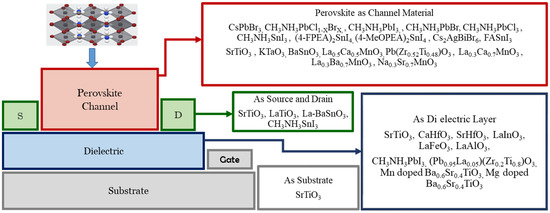
Figure 1 shows various types of perovskite materials, which are used to perform different functions in thin-film FETs. In 1997, the perovskite material La0.7Ca0.3MnO3 (LCMO) was used as a semi-conducting channel, and another perovskite structured PbZr0.2TiO0.8O3 (PZT) was used as a ferroelectric layer in a thin-film FET [14]. However, the introduction of a hybrid double perovskite (C6H5C2H4NH3)2SnI4 ((C6H5C2H4NH3)—phenethyl ammonium (PEA)) in the year of 1999 laid the foundation for the research works on semiconducting perovskite thin-film channel FETs [15]. The perovskite (C6H5C2H4NH3)2SnI4 was used as a semiconductor material in thin-film FETs by a group at the IBM T. J. Watson research center [15][16][15,16] by using different synthetic processes [15]. The highest proportion of perovskite materials has therefore been used as the channel materials in thin-film FETs, as shown in Figure 1.
 In most of the reported perovskite FET works, the FET structure is used to study the charge carrier dynamics and mobility of the perovskite materials [18][17]. However, in the recent past, the perovskite FETs have attracted global attention due to the widespread applications of these perovskite FETs in light detectors [19][18], photo FETs [20][19], light-emitting FETs (LEFET) [21][20], and static and dynamic memory devices [14]. Yet the application of perovskite materials as the channel in FETs needs many further studies to become a potential contender in the commercial market.
2. Fundamentals of Semiconducting Perovskite Semiconductor Materials
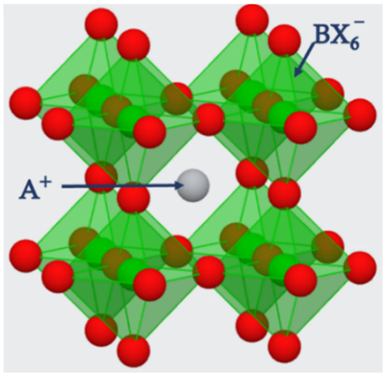
The structure of perovskites is considered octahedral with the generic chemical formula of ABX3. The term perovskite is used to denote the materials existing in the crystal structure of ABX3. Perovskites are bonded in the octahedral shape of corner-sharing structure, which forms a framework of 3D crystal structure as shown in Figure 2.Figure 2. The corner sharing 3D crystal structure of ABX3 perovskite. A⁺ ions embedding the voids of octahedral by sitting in their cavities [171].
Perovskites are extensively used in different dimensions, such as 0D nanoparticles [22][34], 1D nanowires (NW) [23][35], 2D nanosheets [24][36] and single crystals (SC) or thin films [25][26][37,38] in optoelectronic device applications ranging from thin-film light-emitting devices, solar cells and solid-state lasers to thin film FETs. Perovskite semiconductor materials are synthesized by varying the substitutions for each component with different molecular stoichiometry [27][39]. Different cations and anions, which are shown in Figure 3, incorporated with the compositions of the perovskites, dictate the performance of the devices and the fabrication processes as well [1].
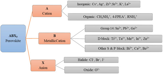
Figure 3. Classification of the different ionic components formulating the compositions of ABX3 3D perovskites for semiconducting channel materials [171].
The certain semiconducting properties such as structure, stability and mobility of the resultant perovskites, composed of the ions stated in Figure 2 depend on the attributes of respective formulating ions. So, the perovskites are classified according to the compositions of ions as single hybrid perovskite, all inorganic perovskite and the double and triple perovskites. For instance, a double perovskite and a triple perovskite can be formulated by the different ions in Figure 3 with multiple stoichiometric compositions.
In a perovskite of ABX3, as the cation of A is surrounded by the eight anionic BX−6 in a three-dimensional cubic shape as shown in Figure 2. The stability of the perovskite materials is decided by the chemical components which formulate the material. Goldschmidt’s tolerance factor t is used as a formula to predict the stability of the perovskite structure.
where RA, RB and RX are the ionic radii of cation A, the divalent metal ion and the halogen ion, respectively. At room temperature, Goldschmidt’s tolerance factor for a stable perovskite cubic structure ranges from 0.89 to 1 [28][29][40,41].
2.1. Hybrid Perovskites
Hybrid perovskite is formulated by substituting organic cations such as methyl ammonium (CH3NH3+), ethyl ammonium (CH3CH2NH3+), 4-fluorophenyl ethyl ammonium 4-FPEA, formamidinium (FA+), 3- amino propyl and other alkyl ammonium ions (RNH3+), etc., in place of A of ABX3 with the metallic (inorganic) cation of B and the halide or oxide anion of X [27][30][31][31,39,42]. Subsequently, these are classified as hybrid (organic-inorganic) perovskites. The metal halide hybrid perovskites are the most exciting materials in optoelectronic applications, as they have shown excellent spectroscopic development [32][33][43,44].
In hybrid perovskites, the organic cation is larger than the metallic ions and has the ability to rearrange the crystal structure as the organic part is bonded by the weak van der Waal interactions and hydrogen bonding [22][23][34,35]. So, the symmetry of the molecule is increased in the hybrid perovskites more than the other types. As a result, the optoelectronic properties of the hybrid perovskites can be fine-tuned by varying the chemical structure [34][45]. The hybrid halide perovskites can be synthesized using simple and easy processes [35][36][46,47]. The instability of these hybrid materials in the exposure to moisture, heat and light in the environment is a major challenge during the fabrication [37][48] and operations of the devices [38][39][49,50], which keeps improving with further studies. However, the limitation in the value of the charge carrier mobility with organic cation barriers [40][51], as it does not vary with the different halogen anions, is considered as another concern to be overcome in the commercialization of devices based on hybrid halide perovskites [18][41][17,52].
2.2. All Inorganic Perovskites
The halide and oxide perovskites, which are formulated with monovalent or divalent inorganic A site cations of the ABX3 prototype, are known as all inorganic perovskites [42][53]. For instance, CsPbBr3, SrTiO3 or KTaO3 are generally categorized as all inorganic perovskites. With the presence of metallic ions, the high carrier mobility along with the narrow emission peak of these types of perovskites is considered an advantage in optoelectronic applications [43][54]. Hence, the device performance using all inorganic perovskite semiconducting materials is massively improved compared to the other types of perovskites [44][45][55,56]. Therefore, all inorganic perovskites are being used in multiple device applications in different structural forms [46][57]. However, the brittleness and the very low colloidal stability of these materials are considered a major challenge during the fabrication of the devices using all inorganic perovskites [47][58].
2.3. Double and Triple Perovskites
The double and triple perovskites have the generic formula of A2M(I)M(III)X6, A2M(IV)X6 or An+1BnX3n+1, which were derived from the ABX3 prototype [48][59]. The double and triple perovskites came into the fold a little later than the single hybrid perovskites in the optoelectronic applications as the charge recombination occurs due to the high exciton-binding energy rather than the charge separation [60][492][50]. However, these types of perovskites are being synthesized to fabricate many different optoelectronic devices [51][61] due to their improved stability to temperature, light and moisture than the single hybrid halide and all inorganic perovskites. The structure-related optoelectronic properties are the main factors to be considered in the fabrication for device applications [52][62]. However, the ion migration hindered by the incorporation of the layers in these perovskites causes lower charge carrier mobilities in the device performances [53][63]. The stability of these types of perovskites was found to be better than the other two types due to their building blocks [54][55][64,65].
3. Perovskite FETs
3.1. Perovskite Thin Film FET Device Structures
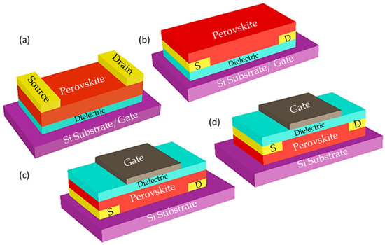
Thin film FET consists of a thin film semiconductor material as the channel. In perovskite thin-film FETs, the channel is generally a polycrystalline thin film made-up of perovskite structured semiconductors. It also consists of two metal electrodes of source S and drain D with Gate electrode of G which is located close to the channel layer. The gate, electrodes and semiconductors can be placed in different positions hence four different device configurations bottom gate top contact (BGTC), bottom gate bottom contact (BGTC) top gate bottom contact (TGBC) top gate top contact (TGTC)) to fulfil the different functional purposes as shown in Figure 4.Figure 4. Device structures of perovskite FETs with four different globally recognized configurations (a) bottom gate top contact (BGTC), (b) bottom gate bottom contact (BGBC), (c) top gate bottom contact (TGBC) and (d) top gate top contact (TGTC) [171].
3.2. Electrical Properties of FETs
A FET can be electrically characterized in two ways: (1) output and (2) transfer characteristics. Among these, the transfer characteristics of the FET can expose its switching characteristics [56][72]. The transfer characteristic of a FET is the variation in the drain-source current Ids under constant drain-source voltage Vds with varying gate voltage Vg.
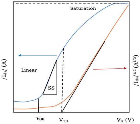
3.2.1. On-Off Ratio
The on-off ratio is an important measure of a FET which indicates the quality of the switching. This is a numerical ratio between the on and off-stage currents through the channel as shown in Figure 56. High on-off ratios indicate that the on currents of the FET are much higher than that of the off current and hence the FET is highly switchable. The off current in ambipolar FETs can be defined as the current when the carrier inversion occurs, thus the minimum current during the transfer sweep.Figure 56.
Transfer characteristics curve of a perovskite thin film FET with linear and saturated regimes
.
3.2.2. Threshold Voltage
The threshold voltage VT of a FET can be defined as the voltage at which the FET turns to the off state from the on state [56][57][72,77] as shown in Figure 6. In an ambipolar FET, the threshold voltage will be the voltage at which the current Ids minimum occurs. In other words, it is the voltage at which the carrier inversion occurs. The region between the turn-on voltage and the threshold voltage is known as the sub-threshold regime in the transfer characteristics curve and the reciprocal slope of the log (Ids) − Vg curve gives the sub-threshold swing, which reflects the speed of switching ability of the device.3.2.3. Mobility Calculations in FETs
The most important intrinsic electrical properties of a semiconductor are its charge carrier mobility and diffusion length [40][51]. A good proportion of the perovskite-based thin film FET studies were carried out to measure the mobility of the semiconducting materials [58][78]. In a perovskite thin-film FET, the field effect mobility μ is considered as the average drifting velocity of the charge carriers in the active semiconducting layer with an applied electric field [59][79]. The efficiency of the FET devices is increased with the charge carrier mobility in the channel, as the drain-source current primarily depends on it [59][79]. The calculation of charge carrier mobility in a semiconducting layer of a perovskite FET is carried out based on the transfer characteristics curve with two important assumptions: (a) mobility does not depend on carrier density, and (b) the transverse gate electric field is much greater than the applied source and drain voltage [60][80].3.3. Early Works (Before 2012) on Perovskite FETs
TBased on the literature, the first research paper on perovskite FET was published in 1999 using a layered bulk (C6H5C2H4NH3)2 SnI4 thin film as the semiconducting channel with Pd as the source and drain electrodes from the IBM T. J. Watson Research Center [15]. The same research group reported (C6H4FC2H4NH3)2SnI4 perovskite thin-film FETs in 2001 [16] and (phenethyl ammonium)2SnI4 in 2002 [61][84]. A group in Kyushu University of Japan continued the work based on (PEA)2SnI4 channel FETs by using different fabrication methods of deposition techniques in 2003 and 2004 [62][63][85,86]. In 2006, the same group turned to the hybrid perovskite of MASnI3 as channel materials in FET [64][87]. Apart from those two groups’ works, the perovskite of PbZr0.52Ti0.48O3 (PZT) was used as channel materials in ferroelectric FETs on two occasions [14][65][14,88].3.4. Recent Works (After 2012) on Perovskite FETs
After the introduction of perovskite materials in solar cells [12][66][12,93], a huge number of perovskite materials have been used as semiconducting active materials in the fabrication of solar cells. In consequence, there is a substantial increase in the number of these since the first MAPbI3 channel-based perovskite FET [67][94]. All the reported perovskite-based thin-film FET studies in the literature after 2012 are classified into three different categories based on the perovskite material types.3.4.1. Hybrid (Organic Inorganic) Perovskite FETs
The hybrid halide perovskites were used in most of the thin film FET studies. Optoelectronic and material properties of tin- and lead-based hybrid perovskites with different organic cations were analysed and MAPbI3 was found as the most promising hybrid perovskite semiconductor than MASnI3, HC(NH2)2SnI3 and HC(NH2)2PbI3 [68][95]. Having organic cations makes the device fabrication easier with single hybrid perovskite materials [61][84].3.4.2. All-Inorganic Perovskite FETs
CsPbBr3 is the most dominant of all inorganic perovskite materials, which was studied in [69][89] many different crystal structures in FET research works. All-inorganic perovskites loaded with CsPbBr3 quantum dots and organic rubrene semiconducting sheets were used, and optical and electronic characteristics were analyzed by Youn et al. [70][132]. In 2019, a phototransistor was fabricated with the semiconducting channels of all inorganic CsPbBr3, and the hole mobility was found to be 0.02 cm2s−1V−1 and 0.34 cm2s−1V−1 in dark and illuminated conditions, respectively, with an excellent ambipolarity [71][133]. The high carrier mobility in the all-inorganic perovskite is improved as the charge carrier mobility is enhanced by the incorporation of inorganic cations of Rb and Cs [72][134].3.4.3. Double and Triple Perovskite FETs
However, the charge carrier mobility is affected by the interlayer distance in these types of perovskites, and the number of FET studies based on double or triple perovskites has increased recently on account of their greater stability than the other two types [73][146]. Perhaps the earliest study of FET was performed based on the double perovskite of (PEA)2SnI4 [15]. Then, the various double and triple perovskite materials were used in different forms for thin-film FET applications. Cs2AgBiBr6 is one of the most popular materials for solar PV applications these days.3.5. Single-Crystalline Perovskite FETs
In a polycrystalline semiconductor material, the presence of grains and grain boundaries causes the screening effect in the field effect mobility [25][37]. However, this effect, which is generated by the heat in the polycrystalline material, is denied in the device applications of single crystalline FET [25][37]. The trap density of single-crystalline perovskites was seen to be lower than polycrystalline perovskites [74][164]. The tunnel junction formations occur due to the passive charge accumulations in the grain boundaries [75][97] in the polycrystalline materials. So, the grain boundary effects are eliminated in single crystalline perovskite FETs, which are less defective than the polycrystalline FETs. However, the poor stability of the single crystalline perovskite materials is a drawback in commercial device applications. The charge transport mechanism in MAPbI3 in single crystalline semiconductors was compared with the polycrystalline FET in [11]. The effect of grain boundaries was reduced in the single crystalline transistor, and the electrical characteristics were recorded to be better in single crystalline FET [76][165]. Electrochemical reactions of Au electrodes in a CH3NH3PbBr3 single-crystal-based FET were investigated in [77][108]. The single MaPbI3 crystal’s photo-generated carrier diffusion was found to be lesser at lower temperatures in [78][114].3.6. Perovskite FETs with Nanostructured Channel
Perovskite nanomaterials are immensely used in device applications. In FETs, the -perovskite nanomaterial is used in two types: (1) single nanostructure FETs and (2) thin-film FETs made up of perovskite nanostructures. The single nanostructure FETs consist of a single nanostructure material as a channel. CsPbX3 nanowires have received significant interest as a material for optoelectronic applications, including flexible light detectors [79][80][166,167].References
- Deschler, F.; Neher, D.; Schmidt-Mende, L. Perovskite semiconductors for next generation optoelectronic applications. APL Mater. 2019, 7, 7–10. Gnanasampanthan Abiram; Murugathas Thanihaichelvan; Punniamoorthy Ravirajan; Dhayalan Velauthapillai; Review on Perovskite Semiconductor Field–Effect Transistors and Their Applications. Nanomaterials 2022, 12, 2396, 10.3390/nano12142396.
- Fu, Y.; Zhu, H.; Chen, J.; Hautzinger, M.P.; Zhu, X.Y.; Jin, S. Metal halide perovskite nanostructures for optoelectronic applications and the study of physical properties. Nat. Rev. Mater. 2019, 4, 169–188. Gnanasampanthan Abiram; Fatemeh Heidari Gourji; Selvakumar Pitchaiya; Punniamoorthy Ravirajan; Thanihaichelvan Murugathas; Dhayalan Velauthapillai; Air processed Cs2AgBiBr6 lead-free double perovskite high-mobility thin-film field-effect transistors. Scientific Reports 2022, 12, 2455, 10.1038/s41598-022-06319-z.
- Rhee, S.; An, K.; Kang, K.T. Recent advances and challenges in halide perovskite crystals in optoelectronic devices from solar cells to other applications. Crystals 2021, 11, 39.
- Rezaee, E.; Kutsarov, D.; Li, B.; Bi, J.; Silva, S.R.P. OPEN A route towards the fabrication of large-scale and high-quality perovskite films for optoelectronic devices. Sci. Rep. 2022, 12, 7411.
- Hao, J.; Xiao, X. Recent Development of Optoelectronic Application Based on Metal Halide Perovskite Nanocrystals. Front. Chem. 2022, 9, 822106.
- Ouedraogo, N.A.N.; Chen, Y.; Xiao, Y.Y.; Meng, Q.; Han, C.B.; Yan, H.; Zhang, Y. Stability of all-inorganic perovskite solar cells. Nano Energy 2020, 67, 104249.
- Li, Z.; Klein, T.R.; Kim, D.H.; Yang, M.; Berry, J.J.; Van Hest, M.F.A.M.; Zhu, K. Scalable fabrication of perovskite solar cells. Nat. Rev. Mater. 2018, 3, 18017.
- Wang, S.; Yousefi Amin, A.A.; Wu, L.; Cao, M.; Zhang, Q.; Ameri, T. Perovskite Nanocrystals: Synthesis, Stability, and Optoelectronic Applications. Small Struct. 2021, 2, 2000124.
- Braga, J.P.; De Lima, G.R.; Gozzi, G.; Santos, L.F. Electrical Characterization of Thin-Film Transistors Based on Solution-Processed Metal Oxides. Des. Simul. Constr. Field Eff. Transistors 2018.
- Zhu, H.; Liu, A.; Noh, Y.Y. Recent progress on metal halide perovskite field-effect transistors. J. Inf. Disp. 2021, 22, 257–268.
- Paulus, F.; Tyznik, C.; Jurchescu, O.D.; Vaynzof, Y. Switched-On: Progress, Challenges, and Opportunities in Metal Halide Perovskite Transistors. Adv. Funct. Mater. 2021, 31, 2101029.
- Kojima, A.; Teshima, K.; Shirai, Y.; Miyasaka, T. Organometal halide perovskites as visible-light sensitizers for photovoltaic cells. J. Am. Chem. Soc. 2009, 131, 6050–6051.
- Mei, Y.; Zhang, C.; Vardeny, Z.V.; Jurchescu, O.D. Electrostatic gating of hybrid halide perovskite field-effect transistors: Balanced ambipolar transport at room-temperature. MRS Commun. 2015, 5, 297–301.
- Mathews, S.; Ramesh, R.; Venkatesan, T.; Benedetto, J. Ferroelectric field effect transistor based on epitaxial perovskite heterostructures. Science 1997, 276, 238–240.
- Kagan, C.R.; Mitzi, D.B.; Dimitrakopoulos, C.D. Organic-inorganic hybrid materials as semiconducting channels in thin-film field-effect transistors. Science 1999, 286, 945–947.
- Mitzi, D.B.; Dimitrakopoulos, C.D.; Kosbar, L.L. Structurally tailored organic-inorganic perovskites: Optical properties and solution-processed channel materials for thin-film transistors. Chem. Mater. 2001, 13, 3728–3740.
- Gnanasampanthan Abiram; Murugathas Thanihaichelvan; Punniamoorthy Ravirajan; Dhayalan Velauthapillai; Review on Perovskite Semiconductor Field–Effect Transistors and Their Applications. Nanomaterials 2022, 12, 2396, 10.3390/nano12142396.
- Motta, C.; El-Mellouhi, F.; Sanvito, S. Charge carrier mobility in hybrid halide perovskites. Sci. Rep. 2015, 5, 12746.
- Miao, J.; Zhang, F. Recent progress on highly sensitive perovskite photodetectors. J. Mater. Chem. C 2019, 7, 1741–1791.
- Wang, J.; Liu, F.; Wang, G.; Wang, L.; Jiang, C. Novel organic-perovskite hybrid structure forward photo field effect transistor. Org. Electron. 2016, 38, 158–163.
- Chin, X.Y.; Cortecchia, D.; Yin, J.; Bruno, A.; Soci, C. Lead iodide perovskite light-emitting field-effect transistor. Nat. Commun. 2015, 6, 7383.
- Schmidt, L.C.; Pertegás, A.; González-Carrero, S.; Malinkiewicz, O.; Agouram, S.; Mínguez Espallargas, G.; Bolink, H.J.; Galian, R.E.; Pérez-Prieto, J. Nontemplate synthesis of CH3NH3PbBr3 perovskite nanoparticles. J. Am. Chem. Soc. 2014, 136, 850–853.
- Horváth, E.; Spina, M.; Szekrényes, Z.; Kamarás, K.; Gaal, R.; Gachet, D.; Forró, L. Nanowires of Methylammonium Lead Iodide (CH3NH3PbI3) prepared by low temperature solution-mediated crystallization. Nano Lett. 2014, 14, 6761–6766.
- Li, P.; Chen, Y.; Yang, T.; Wang, Z.; Lin, H.; Xu, Y.; Li, L.; Mu, H.; Shivananju, B.N.; Zhang, Y.; et al. Two-Dimensional CH3NH3PbI3 Perovskite Nanosheets for Ultrafast Pulsed Fiber Lasers. ACS Appl. Mater. Interfaces 2017, 9, 12759–12765.
- Dang, Y.; Liu, Y.; Sun, Y.; Yuan, D.; Liu, X.; Lu, W.; Liu, G.; Xia, H.; Tao, X. Bulk crystal growth of hybrid perovskite material CH3NH3PbI3. CrystEngComm 2015, 17, 665–670.
- Hamukwaya, S.L.; Hao, H.; Zhao, Z.; Dong, J.; Zhong, T.; Xing, J.; Hao, L.; Mashingaidze, M.M. A Review of Recent Developments in Preparation Methods for Large-Area Perovskite Solar Cells. Coatings 2022, 12, 252.
- Cheng, C.; Zhu, C.; Huang, B.; Zhang, H.; Zhang, H.; Chen, R.; Pei, W.; Chen, Q.; Chen, H. Processing Halide Perovskite Materials with Semiconductor Technology. Adv. Mater. Technol. 2019, 4, 1800729.
- Quan, L.N.; Rand, B.P.; Friend, R.H.; Mhaisalkar, S.G.; Lee, T.W.; Sargent, E.H. Perovskites for Next-Generation Optical Sources. Chem. Rev. 2019, 119, 7444–7477.
- Kang, J.; Cho, J.H. Organic-inorganic hybrid perovskite electronics. Phys. Chem. Chem. Phys. 2020, 22, 13347–13357.
- Gao, W.; Zhu, Y.; Wang, Y.; Yuan, G.; Liu, J.M. A review of flexible perovskite oxide ferroelectric films and their application. J. Mater. 2020, 6, 1–16.
- Wu, Y.; Li, J.; Xu, J.; Du, Y.; Huang, L.; Ni, J.; Cai, H.; Zhang, J. Organic-inorganic hybrid CH3NH3PbI3 perovskite materials as channels in thin-film field-effect transistors. RSC Adv. 2016, 6, 16243–16249.
- Pistor, P.; Ruiz, A.; Cabot, A.; Izquierdo-Roca, V. Advanced Raman Spectroscopy of Methylammonium Lead Iodide: Development of a Non-destructive Characterisation Methodology. Sci. Rep. 2016, 6, 35973.
- Nakada, K.; Matsumoto, Y.; Shimoi, Y.; Yamada, K.; Furukawa, Y. Temperature-dependent evolution of Raman spectra of methylammonium lead halide perovskites, CH3NH3PbX3 (X = I, Br). Molecules 2019, 24, 626.
- Egger, D.A.; Rappe, A.M.; Kronik, L. Hybrid Organic-Inorganic Perovskites on the Move. Acc. Chem. Res. 2016, 49, 573–581.
- Ünlü, F.; Jung, E.; Haddad, J.; Kulkarni, A.; Öz, S.; Choi, H.; Fischer, T.; Chakraborty, S.; Kirchartz, T.; Mathur, S. Understanding the interplay of stability and efficiency in A-site engineered lead halide perovskites. APL Mater. 2020, 8, 070901.
- Ananthakumar, S.; Moorthy Babu, S. Progress on synthesis and applications of hybrid perovskite semiconductor nanomaterials—A review. Synth. Met. 2018, 246, 64–95.
- Senocrate, A.; Kim, G.Y.; Grätzel, M.; Maier, J. Thermochemical Stability of Hybrid Halide Perovskites. ACS Energy Lett. 2019, 4, 2859–2870.
- Deretzis, I.; Smecca, E.; Mannino, G.; La Magna, A.; Miyasaka, T.; Alberti, A. Stability and Degradation in Hybrid Perovskites: Is the Glass Half-Empty or Half-Full? J. Phys. Chem. Lett. 2018, 9, 3000–3007.
- López, C.A.; Abia, C.; Rodrigues, J.E.; Serrano-Sánchez, F.; Nemes, N.M.; Martínez, J.L.; Fernandez-Díaz, M.T.; Biškup, N.; Alvarez-Galván, C.; Carrascoso, F.; et al. Enhanced stability in CH3NH3PbI3 hybrid perovskite from mechano-chemical synthesis: Structural, microstructural and optoelectronic characterization. Sci. Rep. 2020, 10, 11228.
- Xia, C.Q.; Peng, J.; Poncé, S.; Patel, J.B.; Wright, A.D.; Crothers, T.W.; Uller Rothmann, M.; Borchert, J.; Milot, R.L.; Kraus, H.; et al. Limits to Electrical Mobility in Lead-Halide Perovskite Semiconductors. J. Phys. Chem. Lett. 2021, 12, 3607–3617.
- Futscher, M.H.; Milić, J.V. Mixed Conductivity of Hybrid Halide Perovskites: Emerging Opportunities and Challenges. Front. Energy Res. 2021, 9, 629074.
- Assirey, E.A.R. Perovskite synthesis, properties and their related biochemical and industrial application. Saudi Pharm. J. 2019, 27, 817–829.
- Cao, L.; Liu, X.; Li, Y.; Li, X.; Du, L.; Chen, S.; Zhao, S.; Wang, C. Recent progress in all-inorganic metal halide nanostructured perovskites: Materials design, optical properties, and application. Front. Phys. 2021, 16, 33201.
- Gaulding, E.A.; Hao, J.; Kang, H.S.; Miller, E.M.; Habisreutinger, S.N.; Zhao, Q.; Hazarika, A.; Sercel, P.C.; Luther, J.M.; Blackburn, J.L. Conductivity Tuning via Doping with Electron Donating and Withdrawing Molecules in Perovskite CsPbI3 Nanocrystal Films. Adv. Mater. 2019, 31, 1902250.
- Chen, W.; Li, X.; Li, Y.; Li, Y. A review: Crystal growth for high-performance all-inorganic perovskite solar cells. Energy Environ. Sci. 2020, 13, 1971–1996.
- Yang, H.; Zhang, Y.; Pan, J.; Yin, J.; Bakr, O.M.; Mohammed, O.F. Room-Temperature Engineering of All-Inorganic Perovskite Nanocrsytals with Different Dimensionalities. Chem. Mater. 2017, 29, 8978–8982.
- Cho, H.; Kim, Y.H.; Wolf, C.; Lee, H.D.; Lee, T.W. Improving the Stability of Metal Halide Perovskite Materials and Light-Emitting Diodes. Adv. Mater. 2018, 30, 1704587.
- Chu, L.; Ahmad, W.; Liu, W.; Yang, J.; Zhang, R.; Sun, Y.; Yang, J.; Li, X. Lead-Free Halide Double Perovskite Materials: A New Superstar toward Green and Stable Optoelectronic Applications. Nano-Micro Lett. 2019, 11, 16.
- Gnanasampanthan Abiram; Fatemeh Heidari Gourji; Selvakumar Pitchaiya; Punniamoorthy Ravirajan; Thanihaichelvan Murugathas; Dhayalan Velauthapillai; Air processed Cs2AgBiBr6 lead-free double perovskite high-mobility thin-film field-effect transistors. Scientific Reports 2022, 12, 2455, 10.1038/s41598-022-06319-z.
- Ahmad, S.; Kanaujia, P.K.; Beeson, H.J.; Abate, A.; Deschler, F.; Credgington, D.; Steiner, U.; Prakash, G.V.; Baumberg, J.J. Strong Photocurrent from Two-Dimensional Excitons in Solution-Processed Stacked Perovskite Semiconductor Sheets. ACS Appl. Mater. Interfaces 2015, 7, 25227–25236.
- Mir, W.J.; Sheikh, T.; Arfin, H.; Xia, Z.; Nag, A. Lanthanide doping in metal halide perovskite nanocrystals: Spectral shifting, quantum cutting and optoelectronic applications. NPG Asia Mater. 2020, 12, 9.
- Pedesseau, L.; Sapori, D.; Traore, B.; Robles, R.; Fang, H.H.; Loi, M.A.; Tsai, H.; Nie, W.; Blancon, J.C.; Neukirch, A.; et al. Advances and Promises of Layered Halide Hybrid Perovskite Semiconductors. ACS Nano 2016, 10, 9776–9786.
- Herz, L.M. Charge-Carrier Mobilities in Metal Halide Perovskites: Fundamental Mechanisms and Limits. ACS Energy Lett. 2017, 2, 1539–1548.
- Gao, Y.; Wei, Z.; Hsu, S.N.; Boudouris, B.W.; Dou, L. Two-dimensional halide perovskites featuring semiconducting organic building blocks. Mater. Chem. Front. 2020, 4, 3400–3418.
- Fakharuddin, A.; Shabbir, U.; Qiu, W.; Iqbal, T.; Sultan, M.; Heremans, P.; Schmidt-Mende, L. Inorganic and Layered Perovskites for Optoelectronic Devices. Adv. Mater. 2019, 31, 1807095.
- Prew, B.A. Physics of Semiconductor Devices; Wiley-Interscience: Hoboken, NJ, USA, 1975; Volume 26, ISBN 9780470068328.
- Lin, A.; Patil, N.; Ryu, K.; Badmaev, A.; Gomez De Arco, L.; Zhou, C.; Mitra, S.; Philip Wong, H.S. Threshold voltage and on-off ratio tuning for multiple-tube carbon nanotube FETs. IEEE Trans. Nanotechnol. 2009, 8, 4–9.
- Win, L.L.Y.; Taguchi, D.; Manaka, T. Direct observation of carrier transport in organic-inorganic hybrid perovskite thin film by transient photoluminescence imaging measurement. Jpn. J. Appl. Phys. 2019, 58, SBBG18.
- Zeidell, A.M.; Tyznik, C.; Jennings, L.; Zhang, C.; Lee, H.; Guthold, M.; Vardeny, Z.V.; Jurchescu, O.D. Enhanced Charge Transport in Hybrid Perovskite Field-Effect Transistors via Microstructure Control. Adv. Electron. Mater. 2018, 4, 1800316.
- Choi, H.H.; Cho, K.; Frisbie, C.D.; Sirringhaus, H.; Podzorov, V. Critical assessment of charge mobility extraction in FETs. Nat. Mater. 2017, 17, 2–7.
- Mitzi, D.B.; Dimitrakopoulos, C.D.; Rosner, J.; Medeiros, D.R.; Xu, Z.; Noyan, C. Hybrid field-effect transistor based on a low-temperature melt-processed channel layer. Adv. Mater. 2002, 14, 1772–1776.
- Matsushima, T.; Fujita, K.; Tsutsui, T. High field-effect hole mobility in organic-inorganic hybrid thin films prepared by vacuum vapor deposition technique. Jpn. J. Appl. Phys. Part 2 Lett. 2004, 43, L1199.
- Matsushima, T.; Yasuda, T.; Fujita, K.; Tsutsui, T. Organic-inorganic field effect transistor with SnI-based perovskite channel layer using vapor phase deposition technique. Org. Field Eff. Transistors II 2003, 5217, 43.
- Matsushima, T.; Fujita, K.; Tsutsui, T. Preparation of conductive organic-inorganic cubic perovskite thin films by dual-source vacuum vapor deposition. Jpn. J. Appl. Phys. Part 1 Regul. Pap. Short Notes Rev. Pap. 2006, 45, 523–525.
- So, K.S.; Wong, K.H. Fabrication and characteriztion of an all-perovskite ferroelectric field effect transistor based on Pb(Zr0.52Ti0.48)O3/LaSrMnO3 heteroepitaxial structures. Ferroelectrics 2001, 260, 213–218.
- Lee, M.M.; Teuscher, J.; Miyasaka, T.; Murakami, T.N.; Snaith, H.J. Efficient hybrid solar cells based on meso-superstructured organometal halide perovskites. Science 2012, 338, 643–647.
- Labram, J.G.; Fabini, D.H.; Perry, E.E.; Lehner, A.J.; Wang, H.; Glaudell, A.M.; Wu, G.; Evans, H.; Buck, D.; Cotta, R.; et al. Temperature-Dependent Polarization in Field-Effect Transport and Photovoltaic Measurements of Methylammonium Lead Iodide. J. Phys. Chem. Lett. 2015, 6, 3565–3571.
- Stoumpos, C.C.; Malliakas, C.D.; Kanatzidis, M.G. Semiconducting tin and lead iodide perovskites with organic cations: Phase transitions, high mobilities, and near-infrared photoluminescent properties. Inorg. Chem. 2013, 52, 9019–9038.
- Ueno, K.; Inoue, I.H.; Yamada, T.; Akoh, H.; Tokura, Y.; Takagi, H. Field-effect transistor based on KTaO3 perovskite. Appl. Phys. Lett. 2004, 84, 3726–3728.
- Youn, J.; Park, C.J.; Teng, X.; Lee, K.S.; Kim, J.; Joo, J. Energy and charge transfer effects for hybrids of perovskite CsPbBr3 quantum dots on organic semiconducting rubrene nanosheet. Org. Electron. 2019, 65, 243–250.
- Zou, Y.; Li, F.; Zhao, C.; Xing, J.; Yu, Z.; Yu, W.; Guo, C. Anomalous Ambipolar Phototransistors Based on All-Inorganic CsPbBr3 Perovskite at Room Temperature. Adv. Opt. Mater. 2019, 7, 1900676.
- Erodici, M.P.; Pierone, P.J.; Hartono, N.T.P.; Hidalgo, J.; Lai, B.; Buonassisi, T.; Correa-Baena, J.P.; Sher, M.J. Enhanced charge carrier lifetime and mobility as a result of Rb and Cs incorporation in hybrid perovskite. Appl. Phys. Lett. 2021, 118, 063901.
- Li, C.; Yang, J.; Su, F.; Tan, J.; Luo, Y.; Ye, S. Conformational disorder of organic cations tunes the charge carrier mobility in two-dimensional organic-inorganic perovskites. Nat. Commun. 2020, 11, 5481.
- Polavarapu, L.; Nickel, B.; Feldmann, J.; Urban, A.S. Advances in Quantum-Confined Perovskite Nanocrystals for Optoelectronics. Adv. Energy Mater. 2017, 7, 1700267.
- Li, F.; Ma, C.; Wang, H.; Hu, W.; Yu, W.; Sheikh, A.D.; Wu, T. Ambipolar solution-processed hybrid perovskite phototransistors. Nat. Commun. 2015, 6, 8238.
- Senanayak, S.P.; Yang, B.; Thomas, T.H.; Giesbrecht, N.; Huang, W.; Gann, E.; Nair, B.; Goedel, K.; Guha, S.; Moya, X.; et al. Understanding charge transport in lead iodide perovskite thin-film field-effect transistors. Sci. Adv. 2017, 3, 1–11.
- Wang, J.; Senanayak, S.P.; Liu, J.; Hu, Y.; Shi, Y.; Li, Z.; Zhang, C.; Yang, B.; Jiang, L.; Di, D.; et al. Investigation of Electrode Electrochemical Reactions in CH3NH3PbBr3 Perovskite Single-Crystal Field-Effect Transistors. Adv. Mater. 2019, 31, 1902618.
- McClintock, L.; Xiao, R.; Hou, Y.; Gibson, C.; Travaglini, H.C.; Abramovitch, D.; Tan, L.Z.; Senger, R.T.; Fu, Y.; Jin, S.; et al. Temperature and Gate Dependence of Carrier Diffusion in Single Crystal Methylammonium Lead Iodide Perovskite Microstructures. J. Phys. Chem. Lett. 2020, 11, 1000–1006.
- Ho, J.C.; Meng, Y.; Lai, Z.; Li, F.; Wang, W.; Yip, S.P.; Quan, Q.; Bu, X.; Wang, F.; Bao, Y.; et al. Perovskite core−shell nanowire transistors: Interfacial transfer doping and surface passivation. ACS Nano 2020, 14, 12749–12760.
- Gómez, A.; Wang, Q.; Goñi, A.R.; Campoy-Quiles, M.; Abate, A.; Akbulatov, A.F.; Tsarev, S.A.; Elshobaki, M.; Luchkin, S.Y.; Zhidkov, I.S.; et al. Highly stable and efficient all-inorganic lead-free perovskite solar cells with native-oxide passivation. Nat. Commun. 2020, 10, 16.
More