The defact standard of a solar cell is that electric power generation is made at the same place as photoharvesting is performed, i.e., the function of photoharvesting/photoreception is spatially degenerated with that of electric power generation (photo-electroconversion). Here, in this review paper, we investigate how liberated we are when the degeneracy is lifted off. A conventional concentrator system is, in a sense, a system in which the primary photoharvesting place is decoupled from the photo-conversion part, but is too bulky because the two parts are connected three-dimensionally by photons. We propose a two-dimensional photoreceptor-conversion (2DPRC) scheme in which the photoreception part is spatially decoupled from, but is two-dimensionally connected to the photo-conversion part by a redirection waveguide (RWG). The whole system is in an edge-illumination/photoinjection configuration and concentrator system is quite naturally built, and the edge-injection lift off the trade-off between photo-absorption and photo-carrier collection in the conventional solar cell, leading to a possible high conversion efficiency.
- two-dimensional photoreceptor-conversion (2DPRC) s
- concentrator solar cell
- high efficiency
- redirection waveguide
- discrete translational symmetry
1. Introduction
Global warming urges us to think energy- and environmental issues in coherent manners. In this sense the current major power-generation approaches [1] [1] including solar power [2] seem to need a drastic leap for substantial improvements in power conversion efficiency. Many kinds of solar cells [3][4][5][3–5] have been studied, and high conversion efficiency solar cells have attracted much interest.
Typical, so-called mega-solar systems are used as a vast area of land for placing solar panels to generate large amount of electricity as high as tens to hundreds of Mega Watts (i.e., Mega-solar power plant) [6]. Since these systems are a non-concentrator (or “x1” concentrator) system, the key for the high power is nothing but the area of solar cells, because the photo-electric conversion is made exactly at the place where a photon of sunlight hits on the solar panel. Thus, we call this a spatial degeneracy of photoharvesting and photo-electroconversion functions in conventional solar cells or power converters, for which the more the photons/sunlight are received with the wide area of the panel, the more electric power is generated. The degeneracy causes serious problems in achieving stable and efficient power conversion in wireless optical power transmission (OWPT) [7]. When the laser beam travels a couple of miles, the range of the fluctuation is of several centimeters and mean output power of the OWPT system was observed to be very low especially when the photoelectric converter is composed of serially connected photovoltaic devices/solar cells to output a higher voltage [8][9][8,9]. The OWPT, also known as laser power beaming, is an emerging field; for example, for providing a power supply for unmanned aerial vehicles (UAVs) [10] and/or unmanned ground vehicles (UGVs) [11]. In OWPT, photovoltaic devices are of as much importance as in solar power generation systems.
Solar power density on Earth is a little bit too low, and when it is concentrated, the efficiency of solar cells can be improved due the increase in operation voltage. Actually, concentrator solar-cell systems as well as solar thermoelectric power generation have been of importance. In those systems, sunlight is concentrated using mirrors [12][13] [12,13] and/or parabola antennas [14]. In this sense, those systems can be regarded as the primary light-harvesting part is decoupled from the place where photoelectric or thermoelectric conversion is conducted. In other words, the aforementioned spatial degeneracy of light-harvesting and photoelectric conversion is lifted, although those concentrator systems are very huge in volume, because the light passes three-dimensionally from the place of light-harvesting to photoelectric conversion part. Thus, such bulky systems [13], being relatively easy to be installed in desert and dry land, are very hard to introduce in metropolitan areas. Now, it could be revolutionary if we could connect those two parts, i.e., the place of light-harvesting with that of photo-electroconversion, not three-, but two-dimensionally. Once this is done, the situations depicted in Figure 1 become possible, i.e., on one hand, this new scheme serves as a harvester of photons or “summation machine” of photons of any spatial distribution. The new scheme functions as a concentrator solar cell system when the incoming light is spatially uniform like in the case of sunlight. On the other hand, when the incoming light is of the form of Dirac’s d-function, the scheme just simply sums up those d-functions with the zero photon field around them. No matter how many times zero is summed up, it gives zero, i.e., the summation results only care about the number of d-functions, not their positons. In OWPT, a laser beam is, in good approximation, d-function-like. Thus, as depicted in the lower two drawings in Figure 1, the new scheme gives same/identical output no matter where the laser beam arrives at in the detector (RWG), resulting in a robust OWPT system. In an approach to achieve potentially lower cost in solar photovoltaic generation, developed are luminescent solar concentrators (LSCs) [15][16][17][15–17] that, are meant to be used in a similar manner as depicted in Figure 1 for low optical intensity like sunlight, not for laser beams, simply because they penetrate LSCs.
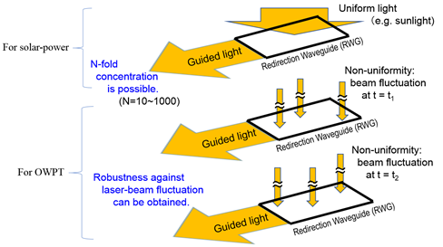
Figure 1. A system with 2D-connected photoreceptor-conversion scheme, which provides us with concentrator solar-cell systems (top figure) as well as an efficient OWPT system that is robust against spatial beam fluctuations as illustrated in bottom two which give the same output at the edge.
2. Two Dimensionally Connected Photoreceptor-conversion Scheme
Thus, we propose a new system in which photoharvesting/photoreception part is spatially decoupled from, but two-dimensionally connected to, photoelectric conversion (photo-conversion) part by thin (2D) waveguide (WG) [18] [18] as depicted in Figure 2. We call this system 2-Dimensionally connected photoreception-photoelectroconversion (or, in short, 2D-PhotoRecepto-Conversion) (2DPRC) scheme. Note that the 2DPRC scheme, realized by redirection waveguide (RWG) consisting of photo-propagation direction converter (PDC) and discrete translational symmetry waveguide (DTSWG), and a planar (2D) waveguide as shown in following chapters, gives a natural concentrator system in which concentration factor is given by the photoharvesting area, L x D, divided by the edge light-injection area, D x d, i.e., L/d, with L, D, and d being the harvesting length, width, and the semiconductor thickness, respectively. By taking, for example, p-i-n structure, d can be set much longer than just 100 nm. Depending on the photocarriers’ lifetime, or crystal quality, d could be as thick as tens of to hundreds of microns letting L be tens to hundreds of millimeters when “x1000” concentration is made for orthogonal photon-photocarrier propagation configuration discussed in Section 2.2.1. Note that the 2DPRC scheme can be applied to conventional millimeters-wide tandem solar cells by utilizing, in RWG, a thicker 2D waveguide that is merged into by DTSWG, in which case L could be in the orders of 1 m to 10 m. Realizing the aforementioned WG is, however, quite challenging because a good WG is supposed to convey light-waves/photons for a long distance from one end to the other without losing them in between, which means it is very hard to harvest photons into the core of the waveguide between the two ends when we think of the time-reversal symmetry of Maxwell’s wave-equation.
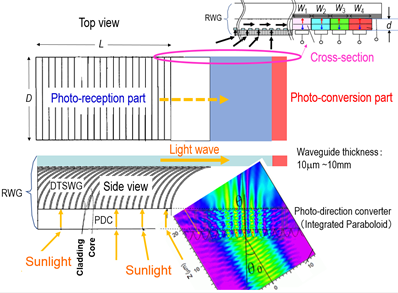
Figure 2. A system with 2D-connected PhotoReceptor-Conversion Scheme (2DPRCS) realized by redirection waveguide (RWG) that consists of photo-propagation direction converter (PDC), discrete translational symmetry waveguide (DTSWG), and a planar (2D) waveguide. Wj (j = 1–4) are the stripe widths. The bottom right inset shows an example of simulation for PDC consisting of paraboloids sheet which is to be superseded by a new structure of “paraboloids + hemispheres” discussed in Section 2.1.1.
2.1. Photoharvesting (Photo-reception) Part
2.1.1. Photopropagation Direction Convertor (PDC) in Redirection Waveguide (RWG)
Photoharvesting or photo-reception part of 2DPRC is composed of redirection waveguide (RWG), in which the sunlight coming from the sky above with various incident angles results in 2D propagating light. The first layer of RWG, the bottom front in the left bottom inset of Figure 2, is so designed as to make the sunlight coming with various tilt angles go perpendicularly upward in Figure 2. The first layer is called photopropagation direction convertor (PDC). The sunlight, via PDC, eventually goes into the 2D waveguide, of the RWG, as shown at the top of the side view in Figure 2. The PDC is obtained using a thin sheet, one side of which is covered with densely packed paraboloids [19]. One of those paraboloids sheet was fabricated using imprinting. In the bottom right of Figure 2, we show a simulation result for a PDC with parabola cross-sectioned structure [20]. In Figure 3, shown are the results of experiments in which LED light is coming from behind the paraboloids sheet, passing through it, and impinges upon a screen 15 mm apart from the paraboloids sheet. Both the height and bottom width of the paraboloid are ~100 mm in the PDC used in the experiment. As shown in Figure 3, for almost all incident angles of the LED light, a strong optical spot is observed on the screen right behind the incident position of the light (indicated by the arrows) on the paraboloids sheet just as in the case for coherent light [21], which demonstrates the coherence is not the key issue for PDC to be able to change the light direction. Further, this result suggests that the PDC, being originally introduced to incorporate morning and/or late-afternoon sunlight effectively, can actually be quite effective for utilizing diffusive light like in cloudy or even rainy days, for which conventional concentrator systems based on lenses do not operate effectively. Except for the intermediate incident angles of around 30 and 40 degrees, the paraboloids sheet used as the PDC of the RWG is demonstrated experimentally to have the aforementioned first function to make 3D photons coming with various angles go almost perpendicularly into the 2D plane of the RWG. For these intermediate incident angles, we have proposed a new structure in which the top of the paraboloid is replaced with a hemisphere. In Figure 4, we have calculated the case in which the cross-section is parabola and semicircle for the sake of simplicity assuming translational symmetry along the y-direction in Figure 4. It is expected that the photons with incident angle of 40 degrees go almost perpendicularly with respect to the sheet plane, thanks to the new PDC composed of paraboloid and hemisphere. For PDC, although it is somewhat difficult to fabricate, “paraboloid + hemisphere” would be better than “paraboloid” only, since the hemisphere provides us with better control of ray geometry.
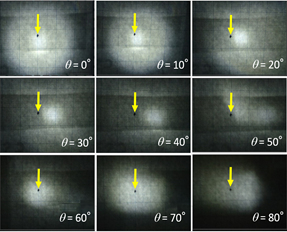
Figure 3. The position of LED light seen from the back of the screen being ~15mm apart from the paraboloids sheet of PDC, behind which the LED is set with various incident angle q with respect to the PDC. The arrows show the center of the incident LED light beam.
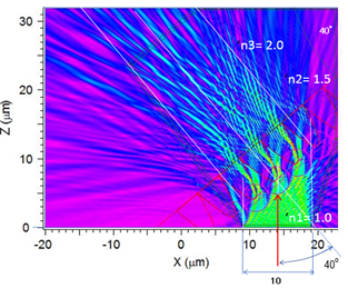
Figure 4. Simulation result of light field for photons with incident angle of 40 degrees. In the new PDC composed of paraboloid and hemisphere.
2.1.2. The 3D-to-2D Conversion of Photons in Redirection Waveguide (RWG)
The second function of the RWG is to make the vertically coming 3D light change into 2D-photons in the thin slab waveguide in the RWG as shown in the middle of Figure 2. Since the equation that governs the electromagnetic field (Maxwell’s wave-equation) has time-reversal symmetry, photons being never lost to outside in the middle of a waveguide means that they, when time-reversed, never come into the WG from outside, either, except for at the WG’s two ends. Actually, our first model system was a diffraction-based redirection waveguide exploiting refractive index modulation which has a symmetric structure and has the fundamental difficulty [22]. Let’s consider the case where the incoming 3D photons are to go into 2D WG and finally hit the photovoltaic device placed at the right end as shown in Figure 5. In general, for any symmetric WG, there are as many left-going photons (LGPs) as right-going photons (RGPs) for incoming 3D photons to go into the 2D waveguide as seen in Figure 5. Now, the fundamental problem is that LGPs can be regarded as time-reversed RGPs and that the symmetric WG, which turns the incoming 3D photons into RGPs, at the same time, lets LGPs go back into 3D space again as denoted by dashed arrow in Figure 5. Thus for the symmetric waveguide, the 3D to 2D convertibility could not be very high because of the synergy of spatial and time-reversal symmetries. Note that luminescent solar concentrators (LSC) [15–17] would not be free from this fundamental limitation either, because the dyes and/or quantum dots are uniformly distributed in the LSCs, which, thus, are in a category of symmetric waveguides.
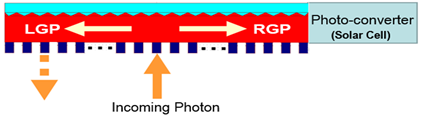
Figure 5. 3D photons going into a spatially symmetric 2D-waveguide equipped with a photoelectric converter at its right end.
Thus, as shown in Figure 6, we are led to a system in which photoharvesting/photoreception part (bottom left of top figure) is spatially decoupled from, but 2D-connected to the photo-conversion part by an asymmetric waveguide. Note that in this new structure, the bottom cladding layer for the 2D waveguide (the main stream), being not spatially continuous as shown in the bottom of Figure 6, gives the 2D waveguide’s core an open geometry. Thus, the core is connected, through the curved tributary waveguides, to the bottom plane where photons come in vertically thanks to the PDC [23], for which an example of corresponding simulation result is shown in the right bottom inset of Figure 2. Thus, proposed is a discrete translational symmetry waveguide (DTSWG) [21], which is in marked contrast to the conventional waveguides and optical fibers that have continuous translational symmetry. Due to the discrete cladding structure, the waveguide can harvest 3D photons coming vertically from beneath in Figure 6, or equivalently, in bottom left of Figure 2. As discussed later in this paper, at the right end of the WG are placed multi-stripe orthogonal photon-photocarrier propagation solar cells (MOP3SC) in which photons propagate in the direction orthogonal to that of the photocarriers [21] as depicted in the top right inset of Figure 2. Simulation of light propagation in the new WG depicted in Figure 2 and Figure 6 is performed with finite difference time domain (FDTD) method [24] and the result is shown in Figure 7, where the refractive index of the core of the mainstream and also tributary curved waveguides is set to be 2.0 and that of the cladding layers 1.35. In this simulation, the period of tributary WG is 2.66 mm with widths of the core and cladding layer being 2.46 mm and 0.4 mm, respectively, and photons with a wavelength of 740 nm come from the bottom end of the curved tributary waveguides as shown in Figure 7. Although we have to be careful about the wavelength –dependence of the refractive index, RWG is of catoptric system, i.e., photons propagate with total reflection through the waveguide, and we would basically be free from severe wavelength-dependence of the 3D-to-2D conversion efficiency of the sunlight, since the aforementioned period of tributary WG is 2.66 mm being much longer than the wavelengths of the most of the major energy-carrying photons in the sunlight. For the 2D WG (main stream), we have set its bottom cladding to be discrete and to touch the mainstream core tangentially as shown in Figure 6. As a result, the light propagation is not much affected by the openness of the core nor by the discreteness of the bottom cladding layer as seen in Figure 7.
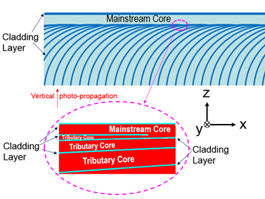
Figure 6. Asymmetric waveguide with discrete translational symmetry (top) and at bottom is enlarged view of the part where the tributary curved WGs merge into the 2D planar WG (mainstream).
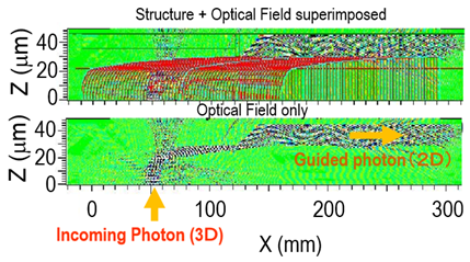
Figure 7. Optical field simulation for the asymmetric waveguide in RWG shown in Figure 6 and in the middle of Fig. 2. Many of the incoming photons from the bottom pass through tributary curved waveguides into the 2D slab (main stream) waveguide (top figure). Only the optical field is excerpted (bottom figure).
2.2. Photo-electro-conversion Part
2.2.1. Edge-injection Configuration
In 2DPRCS, the spatial degeneracy of photoreception and photo-electroconversion functions is lifted, and those two functions are connected through two-dimensional waveguide. Here, the most efficient way of photo-injection into the photo-electroconvertor, i.e., the solar-cell is through its edge, in marked contrast to conventional configurations in which photons impinge on the 2D-face of the solar cell. The merits of edge-injection configuration have been investigated by many groups [25][26][27][28][29][25–29]. In the conventional solar cell, the photon propagation direction depicted by thick solid line is perpendicular to pn junction, where the photo-carriers’ diffusion/drift directions are, thus, parallel to the direction of photon propagation. Thus, in the conventional, on one hand we need a thick semiconductor layer to fully absorb the solar light, but on the other hand we have to make the layer thickness thin enough to collect photo-generated carriers as much as possible, because the carriers have only a finite life time. The conventional solar cells have severe trade-off in determining the semiconductor layer thickness between light absorption and photo-generated carrier collection [19], as shown by thick solid line in Figure 8. In our edge-injection configuration for multi-striped orthogonal photon-photocarrier propagation solar-cell (MOP3SC), however, photons are absorbed in the direction not parallel but vertical to the carrier drift and/or diffusion as shown in Figure 9, and the constraint seen in the conventional solar cells can be lifted off to give the thick dashed line in Figure 8. This is because the photons come into the solar cell through the edge, and propagate along the pn-junction plane in our edge-photoinjection configuration. Since the photocarriers, i.e., the electrons and holes generated by sunlight, move vertical to the pn-junction plane, the direction of photons is orthogonal to that of the photocarriers. In the case of conventional solar cells, it is the best, but difficult, to obtain active layer materials in which absorption coefficient a and mobility are both large enough. In our solar cell, we can virtually forget the issue of low absorption coefficient a by just simply setting the stripe width Wj (j = 1–4) in Figure 9 as
|
Wj > 1/aj |
(1) |
where aj is the absorption coefficient of the j-th semiconductor stripe. The best mode is to set Wj to be 3–6 times 1/aj. By just concentrating on utilizing high mobility materials thanks to the orthogonal photon-photocarrier-propagation mode, we would be able to enjoy the big jump in the efficiency indicated by dashed arrow from the low-lying thick solid-line to the thick dash-dot line sitting high in Figure 8.
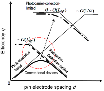
Figure 8. Expected d-dependence of efficiency in the orthogonal photon-photocarrier propagation solar cells. a is the absorption constant, and Ldiff (L’diff) is the diffusion coefficient of photocarriers in the high (low) mobility material.
The RWG is, of course, applicable for both concentrator solar cells and OWPT, and that is the case even when RWG is coupled with the MOP3SC structure shown in Figure 9. For the case of concentrator solar cells, it is obvious because MOP3SC can convert blackbody radiation of the Sun into electricity quite effectively. The merit of using MOP3SC, on the other hand, for OWPT is that we can multitask with a single system, i.e., we can harvest power through the first stripe (having a well-tuned bandgap for the laser beam, with width W1), and also so receive triply superimposed control-signals with longer wavelengths with the three stripes (with widths W2 ~ W4) simultaneously just with the single RWG-coupled MOP3SC shown in Figure 9.
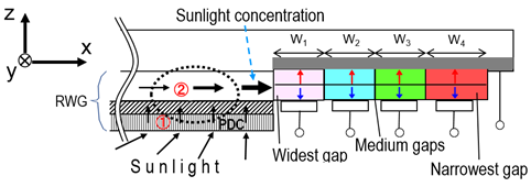
Figure 9. Cross-section of multi-striped orthogonal photon-photocarrier propagation solar-cell (MOP3SC) placed at the right edge of RWG. Region 1 is PDC, and Region 2 encircled by the dashed line is asymmetric DTSWG. RWG consists of DTSWG and PDC. Wj (j =1–4) are the stripe widths of the semiconductors having different bandgaps.
In conventional serially connected tandem structures, usage of a large number of semiconducting materials would be unrealistic, because the same number of pn junctions and accompanying tunnel junctions are necessary. For MOP3SC based on a compound semiconductor InGaN [30][31][30,31], however, it is realistic because such many number of stripes, i.e., various In concentrations in the lateral direction, could be provided in a single epitaxial process, for example, by changing the substrate temperature in that lateral direction in growing InGaN by exploiting the growth temperature dependence of in composition in InGaN layers. Thus, by deliberately giving temperature difference laterally in the substrate, we would be able to obtain graded In composition in a single InGaN growth. Then we placed an electrode in the direction perpendicular to the temperature gradient, i.e., the direction along which the gradient of Indium composition is zero. The number of the electrodes depends on how large the composition difference is, and also on practical lithographical dimensions, which would lead us to fabricate the structure like the one shown in Figure 9 but with continuously varying bandgaps in the lateral direction.
2.2.2. Edge-photoinjection Experiment
For proof-of-the-concept experiment, we have made a structure shown in the inset of Figure 10. Two-hundred-micron thick PEN with 200 nm thick IZO electrode is used as a substrate, on top of which 50 nm thick PEDOT (Poly(3,4-ethylenedioxythiophene) ):PSS (poly(styrenesulfonate)) film and P3HT (poly (3-hexylthiophene)):PCBM ((6,6)-phenyl-C61-buteric acid methyl ester) layer with thickness d = 50–130 nm are spin-coated. Then Al electrode is prepared finally by vacuum evaporation. The sample is illuminated using a green laser having wavelength λ= 532 nm and power of ~1mW. The light is shed from two different directions: one is a conventional illumination configuration in which photons impinge on the structure perpendicularly with respect to the layers and the other is, as the thick arrow shows, the edge illumination configuration for which a modified system of microscopic photoluminescence (PL) is used with its focus on the edge surface. The laser spot size, there, is roughly 30 mm in diameter with tailing skirt-part included, but its strongest spot size is much sharper, a couple of microns in width. Because of this inherent spot size and the Gaussian beam waist located at the edge with focal depth of about 1 mm, we can observe that well-focused excitation photons are made and go along the layer of P3HT:PCBM in the sample starting from the edge [32]. Although the current is not so large as noticed by minute hysteresis in Figure 10, we do observe the photovoltaic characteristics under the edge illumination as shown in Figure 10. Both in the dark and under the edge illumination, we have measured the I-V curve of the cell, and obtained open circuit voltages Voc’s and short circuit current Isc’s. For comparison, we also have measured I-V characteristics using the same solar cell sample under the conventional vertical illumination configuration.
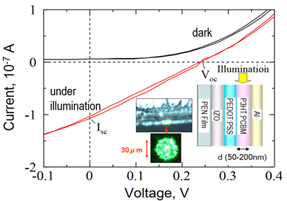
Figure 10. I-V characteristics of the cell in the dark and edge-illumination configuration. Left top inset is the front view of the edge facet, left bottom inset is the beam shed on the edge, and right inset shows the illumination configuration. (Reproduced from [32], Engineering Research Publication, 2016).
Based on those measurements, we plot the product Isc·Voc (∝ η: conversion efficiency) as function of the active-layer thickness d in Figure 11. Blank circles are for the data obtained under conventional illumination and solid circles under the edge illumination. We can see in Figure 11 that Isc·Voc start to decrease for d > 100 nm and is good agreement with the d-dependence of the conversion efficiency observed using the same active-layer materials [33]. In Figure 11, dashed is a line of log d, and the solid line is corresponding to the dependence of exp(−d/L) with L = 30 nm, which is in good accord with what was obtained before when considering the active-layer preparation. Reported was a strong dependence of efficiency from bimolecular recombination, arising from the photoconversion of light at high intensity [34], but this effect equally affect the data points for edge-illumination in Figure 11 because the beam size is larger than d’s for those devices. We can virtually neglect this effect when we discuss the relative d-dependence of the conversion efficiencies in the edge-illumination configuration. The blank circles are, to a fairly good approximation, on the dashed line for d ≤ 100 nm , and the solid circles are well on the solid line for d ≥ 100 nm, which is understood, using Figure 8 (especially for the region encircled by red dashed line where the photo-absorption-limited and photocarrier-collection-limited lines are crossed) that the trade-off (denoted by the thick solid line) seen in the conventional illumination regime is lifted off in the edge illumination configuration, or in the orthogonal photon-photocarrier-propagation mode, as depicted by the thick dashed line in Figure 8. In this mode, the conversion efficiency η, remain high for a small d region for which the conventional illumination (or parallel photon-photocarrier-propagation mode) gives low η because of the loss of photons due to their penetration through the thin active-layers. This result manifests the superiority of the orthogonal photon-photocarrier propagation solar cell anticipated in Figure 8. In the multi-striped orthogonal photon-photocarrier propagation solar cell (MOP3SC), we can concentrate on utilizing high mobility materials getting free from the constraint on α by making the stripe width several times 1/α, and would fully enjoy high conversion efficiency depicted by dash-dot line in Figure 8. The MOP3SC, being coupled to the RWG is of much importance for the next generation of solar cells with a possible high efficiency.
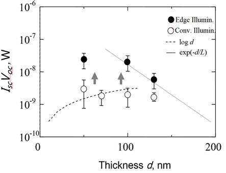
Figure 11. Conversion efficiency vs. active-layer thickness (or electrode spacing) d, under two different illumination configurations (Reproduced from [32], Engineering Research Publication, 2016).
Figure 12 shows the edge-injection experiment in which photons run parallel to pn-junction of Si solar cell. In this experiment a prism and thin film waveguide are used. We have observed photovoltaics in this configuration. Note that the I-V characteristics with laser on but prism off is almost the same as that without laser beam, which indicates how important it is to have a good coupling of the 2D-waveguide with MOP3SC.
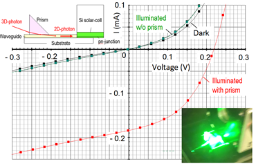
Figure 12. Edge-injection experiment in which photons run parallel to pn-junction of Si solar cell. We have observed photovoltaics in this configuration. In this experiment, a prism and thin film waveguide are used.
2.2.3. Limiting Conversion Efficiency Calculation
We have estimated the conversion efficiency of the MOP3SC using graphical method [35][36] [35,36] using the equation,
|
, |
(2) |
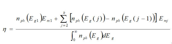
where nph(Eg) is the solar flux absorbed by a semiconductor with energy-gap Eg. Figure 13 shows limiting energy conversion efficiency as a function of the number of semiconductor stripes for solar concentration of 1 sun and 1000 suns under AM1.5 condition [37][38][37,38]. We expect that the new solar cell could convert virtually the whole spectrum of solar light into electricity by choosing semiconductors with appropriate energy gap.
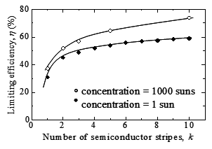
Figure 13. Limiting energy conversion efficiency of the MOP3SC (Reproduced from [38], the union of ecodesigners,2009).
The fact that the multi-stripes can be prepared by a single process in MOP3SC provides us with the strong advantage over the conventional tandem solar cells as well as a unique feature that the each stripe (cell component) in MOP3SC is in parallel connection configuration to each other. This means that indeed high efficiency can be obtained with MOP3SC as shown in Figure 13, but each cell component gives different output voltage. From device-applicational point of view, outputs with small current amounts at different voltages would not be convenient.
As a countermeasure to this problem, we propose to prepare two sets of k-striped MOP3SC, i.e., MOP3SC 1 and MOP3SC 2. The MOP3SC 1 shown in Figure 14 is in common p-metal configuration, while MOP3SC 2 has a common n-metal. For both MOP3SC 1 and MOP3SC 2, the energy gap of j-th stripe (from the left end in Figure 9 where the photons come in), Eg(j) is set
|
Eg(j) = Eg max – (j–1)ΔE, (j = 1–k) |
(3) |
where ΔE = (Eg max–Eg min)/k with Eg max = Eg(1) and Eg min = Eg(k) by definition. Component unit cells in MOP3SC 1 and MOP3SC 2 are connected in such a way that the j-th component cell in MOP3SC 1 with the (k−j + 1)-th in MOP3SC 2 as shown to the right of Figure 14 (for the case of k = 4). Now, the output voltage Vj from the serially connected components is
|
Vj = {Eg(j) + Eg(k–j + 1)}/e = {Eg max–(j–1)ΔE + Eg max–(k–j)ΔE }/e = {Eg max + E gmax–(k–1)ΔE }/e = (Eg(1) + Eg(k))/e = const. (independent of j), |
(4) |
where e is the electronic charge. Thus, each of those k serially connected component cells output, in common, a single constant voltage (Eg max + Eg min)/e. In contrast to a hot carrier solar cell that needs to utilize large excess kinetic energy of the photo-generated carriers before they relax, our new solar cell does not, thanks to the MOP3SC structure.
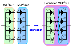
Figure 14. Connected MOP3SC (Reproduced from[38] [38], the union of ecodesigners,2009).
Limiting conversion efficiency of connected MOP3SC is as follows. In Figure 15 the area under the nph(Eg) curve (dashed line) is just equal to the total solar power per unit area. As shown in Figure 15, Emj corresponds to the energy per photon delivered to the load at the maximum power point [21] with respect to the j-th stripe. Here, because of the connection scheme shown in Figure 14 (for k = 4), we have to calculate limiting energy conversion efficiency by maximizing the area of rectangles in Figure 15, based upon Equation (2), treating Eg(j) as variable parameters with the constraint with respect to current,
|
Ij = Ik-j+1 (for j = 1~k), |
(5) |
where Ij is the current flowing the j-th component cell in MOP3SC, and also the constraint on voltage
|
V = {Eg(j) + E g(k-j+1)} (for |
(6) |
 )
)With the optimized Eg(j) thus obtained, we show, in the inset of Figure 15, the limiting energy conversion efficiency as a function of the number of semiconductor stripes k for the connected MOP3SC. We found that when the energy gap is carefully selected, the efficiency of the connected MOP3SC is almost as high as that of single MOP3SC given in Figure 13.
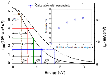
Figure 15. Optimum energy-gap selection for connected MOP3SC (for k = 4) (Reproduced from [38], the union of ecodesigners,2009).