Your browser does not fully support modern features. Please upgrade for a smoother experience.
Please note this is a comparison between Version 2 by Conner Chen and Version 1 by Junjie Li.
Just like rigid templates, there are numerous types of soft templates, including electron resist polymer, photoresist polymer, and various assembled polymers consisting of block polymer, fiber or membrane, polystyrene (PS) sphere, and so forth. These versatile soft templates can be used in the ALA method and have broad prospects for development in powerful fabrication of multiple nanostructures, which possess a lot of advantages, such as simple process, good flexibility, repeatable simplicity of the process, and environmentally friendly easy elimination of the templates, resulting in diversiform 3D nanostructures with numerous device applications.
- atomic layer deposition
- sacrificial templates
- 3D nanostructures
1. Resist Polymer Templates
Due to the utilization of direct writing techniques, resist templates, including electron resists and photoresists, maybe the most flexible and controllable templates for 3D nanostructure fabrication based on ALA method. Nowadays, miniaturized conventional systems require the development of custom applications in imaging, displaying, and spectroscopy, especially for 3D nanosystems and 3D nanostructures. As a result, electron and photoresist templates, which could achieve 3D nanostructures by electron beam lithography (EBL) and direct laser writhing (DLW), are proposed and investigated in many fields, and their fabrication processes are illustrated in Figure 71a,d, respectively. Firstly, the electron or photoresists are patterned by EBL or DLW, and then ALD is applied to fill or coat the obtained templates to assemble 3D nanostructures which are confined by templates. Followed by the removal of the cap of the coated template and exposing residual resist polymer, the resist polymer is removed by O2 plasma or remover.
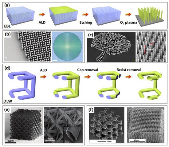
Figure 71. Resist polymer templates by EBL and DLW processes are used to fabricate various 3D nanostructures based on ALA method. (a) The illustrated process routine of 3D nanostructures based on electron resist templates through EBL technique. (b) SEM and optical images of the fabricated metalens. (c) SEM images of the tree-shaped irregular nanostructures and nanotubes with ultra-high aspect ratio of more than 80:1, based on ALA method through electron resist templates by EBL technique. (d) The illustrated process routine of 3D nanostructures based on photoresist templates by DLW technique using ALA method. (e) Overall and enlarged SEM images of the overall alumina octet-truss nanolattice through photoresist by DLW technique based on ALA method. (f) SEM images of two kinds gyroid photonic crystals through photoresist by DLW technique based on ALA method.
In 2016, a novel process for fabricating dielectric metasurfaces through soft electron resist templates based on ALA method was first proposed, which could produce anisotropic, subwavelength-spaced 3D nanostructures with shape birefringence [53][1]. They patterned the electron resist using EBL firstly, resulting in templates with patterns in reverse of the final metasurface. Similar to the process to fabricate 3D nanostructures as discussed above, ALD-based TiO2 films were coated on the template, followed by the removal of TiO2 cap and residual resist, high performance 3D nanofin metasurface as a metalens, as shown in Figure 71b, was successfully fabricated and showed widespread applications in laser-based microscopy, imaging, and spectroscopy. This ALA process should be the simplest strategy to realize the complex 3D nanostructures of dielectric metamaterials up to now, which is also capable of achieving any high-efficiency metasurface optical element. Geng et al. developed the ALA method deeper to fabricate 3D nanostructures utilizing electron beam resist, resulting in large-scale arrays of multiple complex 3D nanostructures with high resolution down to nanometers and ultra-high aspect ratio of hundreds. Particularly, an extreme structural nanotube array with ultra-high aspect ratio of more than 80:1 (8 nm wall thickness and 650 nm height) is assembled successfully. The results are displayed in Figure 71c [54][2].
Creating lightweight, mechanically robust materials has long been an engineering pursuit. Many siliceous skeleton species, such as diatoms, sea sponges, and radiolarians, have remarkably high strengths compared with man-made materials of the same composition, yet are able to remain lightweight and porous [55,56][3][4]. As shown in Figure 71e [57][5], to investigate the lightweight nanostructures, creation of ceramic nanolattices begins with the design and writing of a negative photoresist template using two-photon lithography direct laser writing (DLW), achieving a polymer sacrificial template. Al2O3 film is then deposited onto the soft template by ALD, so that it coats the entire surface of this 3D skeleton. Then the internal polymer is etched away in O2 plasma after the removal of the outermost sides of the coated structure by focused ion beam milling (FIB), resulting in 3D ceramic nanolattice consisting of a network of hollow tubes, which can recover their original shape after compressions in excess of 50% strain. This fabrication method enabled the creation of 3D structures with numerous geometries and custom designs, exhibiting a strong, ultralight, energy-absorbing, and recoverable metamaterial, called a mechanical metamaterial. Using a similar technique based on a photoresist template, gyroid photonic crystals were fabricated successfully, as shown in Figure 71f, which exhibited a complete bandgap in infrared spectroscopy measurements [58][6].
Due to the fact that it commonly relied on negative resists using two-photon lithography, the 3D nanostructure fabrications based on photoresist are limited [59[7][8],60], whose topography and size are restricted. Consequentially, electron resist shows more advantages than DLW photoresist in fabricating 3D nanostructures based on ALA method, which can maximize the virtues of following ALD process in flexible custom topography, precise size control, and more compatibility, further showing giant applications in various optical devices [61,62,63,64,65,66,67,68][9][10][11][12][13][14][15][16]. Despite the long-time consumption, the fabrication of 3D structures through resist polymers by ALA method shows incomparable flexibilities and great compatibility with conventional semiconductor processes, showing ability in achieving arbitrary custom pattern and complicated 3D structures with extreme geometries. New techniques combined with ALA method, like nanoprinting and multibeam exposing, should be developed to reduce the time consumption.
Apart from EBL and DLW, several other techniques could be utilized to pattern resist templates. As presented in Figure 82a, two feasible techniques to pattern photoresist templates are the proximity field nanopatterning (PnP) technique and multibeam interference lithography (MBIL).
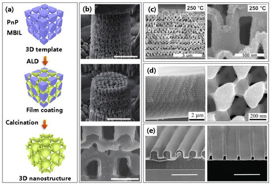
Figure 82. Other photoresist polymer templates by PnP and MBIL processes are used to fabricate 3D nanostructures by ALA methods. (a) Illustrated process routine of 3D nanostructures based on photoresist templates by PnP and MBIL techniques. The two techniques commonly share the same fabrication process, except the methods to fabricate resist templates. (b) SEM images of Al2O3 nano-architectures based on PnP technique taken before and after compression tests. And the enlarged SEM images of Al2O3 nano-architectures. (c) SEM images of 3D ZnO hollow nanostructure deposited at 250 °C after removal of the epoxy template based on PnP method. (d) 3D TiO2 photonic crystals after removal of the polymeric template by MBIL method. (e) SEM images of polymer grating template by MBIL method with Platinum film by ALD; and free-standing Pt nano-accordions after removal of the template.
PnP is a versatile 3D nanopatterning technique that creates highly ordered 3D nanostructures in photosensitive materials by capturing the 3D light distribution, generated by a phase mask with periodic relief structures. The 3D light intensity distribution, called the Talbot effect or self-imaging effect [69[17][18],70], has periodically repeated images generated by interferences of diffracted beams. This method can rapidly fabricate 3D nanostructures through only single exposure over a large area (>1 inch2) [71][19]. As displayed in Figure 82b, hollow-tube-based 3D Al2O3 nanoarchitectures functionalized as lightweight materials were fabricated in large areas using PnP and ALA process [72][20]. The first two SEM images show nanoarchitectures taken during compression and after complete unloading, which revealed that the strengths of these nanoarchitecture materials were powerful. The zoomed-in image of the single unit cell is exhibited in the bottom of Figure 82b. Another group [73][21] reported a truss-like 3D hollow ZnO nanostructure using PnP method that exhibits a drastically improved elastic strain limit while maintaining a piezoelectric coefficient similar to that of single crystal ZnO, showing excellent potential application in enhanced haptic devices, flexible sensors, and energy harvesters. The SEM images of 3D ZnO hollow nanostructures after removal of the epoxy template are displayed in Figure 82c.
Unlike PnP method, multibeam interference lithography (MBIL) is a maskless and practical fabrication technique of periodic microstructures over large areas [76,77][22][23]. This technique possesses advantages of low cost, no contamination, and fabricating pattern over a large area (up to mm in diameter), but the variety of the patterns is limited due to the exposure mechanism of MBIL, such as an anisotropic and aperiodic structure cannot be achieved by this method. By recording four-beam interference pattern into photoresist, a periodical pillar array is obtained as the sacrificial template [78][24], which can be used to form microlenses [79[25][26],80], optical biosensors [81][27], or microaxicons for beam generation [82][28]. The production and optical characterization of a high-quality, high-index 3D photonic crystal using MBIL and ALD was first demonstrated in 2006 [74][29]. A high-quality photonic crystal in amorphous TiO2 was produced after removal of the polymer template, showing potential applications in all-optical circuits, microcavity-based light emitters, and other microstructured photonic devices, as shown in Figure 82d. Min et al. [75][30] also prepared complex Pt nano-accordion structures using a combination of MBIL and ALA; these metal nanostructures have good structural stability and electrical conductivity, as shown in Figure 82e, and their cross sectional profiles can be designed by specifying the template geometry, showing applications in stretchable electronics, photonics, and nanofluidics.
PnP and MBIL methods consume less time than EBL and DLW techniques, which reduces the fabrication cost greatly. Remarkably, there is also no anisotropic volume shrinkage occurring during the calcination to remove the template in the fabrication by PnP and MBIL, providing beneficial optical properties and mechanical stability, showing potential applications for highly efficient gas sensors by utilizing high porosity and large surface area. However, the simplex and inflexible morphologies by PnP and MBIL show less flexibility and controllability, which may limit the application area.
2. Assembled Polymer Templates
As well as resist polymers, alternative soft templates can be the variously assembled polymer templates, which generally include a wide variety of high polymers of electrospinning fibers (ESF), blocked polymer (BCP), and self-assembly polystyrene spheres (PSS), and so forth. Obviously, ESF were fabricated by electrospinning technique, and self-assembly technique is applied to obtain the BCP and PSS templates. The 3D nanostructure fabrication processes based on ALA method through ESF, BCP, and PSS templates are similar, which firstly are the preparation of templates by corresponding techniques, followed by film deposition by ALD, and removal of templates by calcination, as shown in Figure 9a.
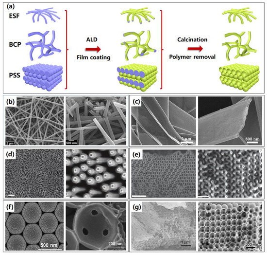
Figure 93. Typical assembled polymer templates are combined with ALA method to fabricate 3D nanostructures. (a) The illustrated process routines of 3D nanostructures based on assembled polymer templates through electrospinning fibers (ESF), blocked polymer (BCP), and polystyrene spheres (PSS) templates. (b) Representative SEM images of AlN hollow nanofibers based on electrospinning after calcination. (c) Overall and cross section SEM images of belt-like BiVO4@ZnO heterojunction based on electrospinning after calcination. (d) Overall and enlarged SEM images of the nanorockets array based on BCP technique. (e) SEM images of two kinds of mesoporous ZnO networks based on BCP technique. (f) Overall and cross section SEM images of TiO2 inverse opals based on self-assembled PS spheres. (g) SEM images of based TiO2 inverse opals on self-assembled PS spheres.
The major advantages of the electrospinning process are easy operating and cost-effective to implement. The wide band gap semiconductors based on electrospinning through the ALA method, such as ZnO [88[31][32],89], SnO2 [90[33][34],91], and TiO2 [88[31][35],92], including CuO [93][36], depicted unique surface functionalities and higher sensitivities toward ethanol, O2 [89[32][37],94], NO2 [91[34][35],92], CO [92,94][35][37], NH3 [88[31][33],90], H2 [90[33][38],95], and so forth. As a result, the 3D nanostructures based on electrospinning toward sensors were widely investigated. Haider et al. [83][39] reported fabrication and characterization of aluminum nitride (AlN)/boron nitride (BN) bishell hollow nanofibers through successive ALD of AlN and sequential chemical vapor deposition (CVD) of BN on electrospinning polymeric nanofibrous sacrificial templates, which are exhibited in Figure 93b. This specific structure might find potential use in composite reinforcement, chemical sensing, and gas adsorption. In addition to sensors, nanofibers based on electrospinning and ALA also displayed enhanced photocatalytic activity in water splitting [96,97][40][41]. The fabrication of BiVO4@ZnO heterojunction with a novel nanostructure for water splitting via electrospinning and ALA techniques were investigated [84][42], as shown in Figure 93c. The belt-like 3D structure exhibited enhanced photoelectrochemical performance and showed potential applications in solar cells. There are plenty of low-cost polymer materials to form polymer fiber templates using electrospinning; they could be polyacrylonitrile (PNA) [95[38][43],98], Nylon [99[44][45],100], polyvinyl acetate (PVA) [92[35][36],93], or Poly (vinylpyrrolidone) (PVP) [84,101][42][46], which show great opportunities in commercial applications.
Another important assembled polymer template for fabricating 3D nanostructures is the blocked polymer (BCP). The blocked copolymer template-assisted method, which is based on a self-assembly process, can generate well-ordered arrays with small feature sizes of 5–50 nm in dot, line, hole, or lamellar patterns, and has been extensively explored as a strategy to form periodic nanostructures [102,103][47][48]. BCP combined with ALA for wafer-scale to fabricate ultrasmall coaxial TiO2/Pt nanotubes was reported, which is used as a catalytic rocket with a length below 150 nm and a tubular reactor size of only 20 nm, leading to the smallest man-made rocket engine reported to date, as shown in Figure 93d [6][49], demonstrating abilities to efficiently power the directional transport of significantly larger passive cargo. Two other different morphologies based on the self-assembly of BCP were synthesized to fabricate mesoporous ZnO networks, as shown in Figure 93e [85][50]. The manufacture of ZnO-based solar cells also showed the feasibility of the integration of the 3D mesostructured ZnO networks into photovoltaic devices.
3D nanostructure could also be formed by the inverse opal (IO) structures, which possess size adjustable pore structure, large surface area, and optical properties of photonic crystals. The inverse opal nanostructures are usually fabricated using a template of silica [50][51] or polymer micro-spheres by the self-assembly route. Polystyrene sphere (PSS) templates are most commonly used and easily removed by calcination. Inverse opal TiO2 nanostructures [86][52] were synthesized by ALA using a template with ordered layers of PS spheres deposited on a Si substrate by spin coating, as illustrated in Figure 93f, where the IO nanostructures showed giant photocatalytic enhancement for the degradation of methylene blue than that of planar TiO2 films. Similarly, a TiO2/MoS2 core/shell inverse opal structure was fabricated based on ALA on a self-assembled multilayer PSS template, as presented in Figure 93g. As a 3D photonic crystal, the TiO2/MoS2 inverse opal structure exhibited obvious stopband reflecting peaks, which can be adjusted through changing the opal diameters as well as the thickness of the MoS2 layer [87][53]. The inverse opal structures could find plenty more applications in photocatalytic [104[54][55],105], solar cells [106[56][57],107], chemical sensors [108[58][59],109], surface enhanced Raman scattering (SERS) detection [110,111][60][61], etc.
The advantage of the ESF, BCP, and PSS template assisted methods should be that no complex and expensive equipment are applied to prepare the templates, as well as easy modification and feasibility of industrial-level high-volume mass production.
References
- Khorasaninejad, M.; Chen, W.T.; Devlin, R.C.; Oh, J.; Zhu, A.Y.; Capasso, F. Metalenses at visible wavelengths: Diffraction-limited focusing and subwavelength resolution imaging. Science 2016, 352, 1190–1194.
- Geng, G.; Zhu, W.; Pan, R.; Zhang, Z.; Gu, C.; Li, J. Precise tailoring of multiple nanostructures based on atomic layer assembly via versatile soft-templates. Nano Today 2021, 38, 101145.
- Kröger, N. Prescribing diatom morphology: Toward genetic engineering of biological nanomaterials. Curr. Opin. Chem. Biol. 2007, 11, 662–669.
- Yang, W.; Chen, I.H.; Gludovatz, B.; Zimmermann, E.A.; Ritchie, R.O.; Meyers, M.A. Natural Flexible Dermal Armor. Adv. Mater. 2013, 25, 31–48.
- Meza, L.R.; Das, S.; Greer, J.R. Strong, lightweight, and recoverable three-dimensional ceramic nanolattices. Science 2014, 345, 1322–1326.
- Peng, S.; Zhang, R.; Chen, V.H.; Khabiboulline, E.T.; Braun, P.; Atwater, H.A. Three-Dimensional Single Gyroid Photonic Crystals with a Mid-Infrared Bandgap. ACS Photon. 2016, 3, 1131–1137.
- Frölich, A.; Fischer, J.; Zebrowski, T.; Busch, K.; Wegener, M. Titania Woodpiles with Complete Three-Dimensional Photonic Bandgaps in the Visible. Adv. Mater. 2013, 25, 3588–3592.
- Kawata, S.; Sun, H.; Tanaka, T.; Takada, K. Finer features for functional microdevices. Nature 2001, 412, 697–698.
- Shi, Z.; Khorasaninejad, M.; Huang, Y.-W.; Roques-Carmes, C.; Zhu, A.Y.; Chen, W.T.; Sanjeev, V.; Ding, Z.-W.; Tamagnone, M.; Chaudhary, K.; et al. Single-Layer Metasurface with Controllable Multiwavelength Functions. Nano Lett. 2018, 18, 2420–2427.
- Devlin, R.C.; Ambrosio, A.; Wintz, D.; Oscurato, S.L.; Zhu, A.Y.; Khorasaninejad, M.; Oh, J.; Maddalena, P.; Capasso, F. Spin-to-orbital angular momentum conversion in dielectric metasurfaces. Opt. Express 2017, 25, 377–393.
- Khorasaninejad, M.; Chen, W.T.; Zhu, A.Y.; Oh, J.; Devlin, R.C.; Rousso, D.; Capasso, F. Multispectral Chiral Imaging with a Metalens. Nano Lett. 2016, 16, 4595–4600.
- Liang, H.; Lin, Q.; Xie, X.; Sun, Q.; Wang, Y.; Zhou, L.; Liu, L.; Yu, X.; Zhou, J.; Krauss, T.F.; et al. Ultrahigh Numerical Aperture Metalens at Visible Wavelengths. Nano Lett. 2018, 18, 4460–4466.
- Devlin, R.C.; Khorasaninejad, M.; Chen, W.T.; Oh, J.; Capasso, F. Broadband high-efficiency dielectric metasurfaces for the visible spectrum. Proc. Natl. Acad. Sci. USA 2016, 113, 10473–10478.
- Mueller, J.P.B.; Rubin, N.A.; Devlin, R.C.; Groever, B.; Capasso, F. Metasurface Polarization Optics: Independent Phase Control of Arbitrary Orthogonal States of Polarization. Phys. Rev. Lett. 2017, 118, 113901.
- Wen, D.; Cadusch, J.J.; Meng, J.; Crozier, K.B. Multifunctional Dielectric Metasurfaces Consisting of Color Holograms Encoded into Color Printed Images. Adv. Funct. Mater. 2020, 30, 1906415.
- Zhang, C.; Divitt, S.; Fan, Q.; Zhu, W.; Agrawal, A.; Lu, Y.; Xu, T.; Lezec, H.J. Low-loss metasurface optics down to the deep ultraviolet region. Light. Sci. Appl. 2020, 9, 1–10.
- Ahn, C.; Park, J.; Kim, D.; Jeon, S. Monolithic 3D titania with ultrathin nanoshell structures for enhanced photocatalytic activity and recyclability. Nanoscale 2013, 5, 10384–10389.
- Latimer, P.; Crouse, R.F. Talbot effect reinterpreted. Appl. Opt. 1992, 31, 80–89.
- Park, J.; Wang, S.; Li, M.; Ahn, C.; Hyun, J.K.; Kim, D.S.; Kim, D.K.; Rogers, J.A.; Huang, Y.; Jeon, S. Three-dimensional nanonetworks for giant stretchability in dielectrics and conductors. Nat. Commun. 2012, 3, 916.
- Na, Y.-E.; Shin, D.; Kim, K.; Ahn, C.; Jeon, S.; Jang, D. Emergence of New Density-Strength Scaling Law in 3D Hollow Ceramic Nanoarchitectures. Small 2018, 14, 1802239.
- Kim, H.; Yun, S.; Kim, K.; Kim, W.; Ryu, J.; Nam, H.G.; Han, S.M.; Jeon, S.; Hong, S. Breaking the elastic limit of piezoelectric ce-ramics using nanostructures: A case study using ZnO. Nano Energy 2020, 78, 105259.
- Stankevičius, E.; Daugnoraitė, E.; Račiukaitis, G. Mechanism of pillars formation using four-beam interference lithography. Opt. Lasers Eng. 2019, 116, 41–46.
- Gedvilas, M.; Indrišiūnas, S.; Voisiat, B.; Stankevičius, E.; Selskis, A.; Račiukaitis, G. Nanoscale thermal diffusion during the laser interference ablation using femto-, pico-, and nanosecond pulses in silicon. Phys. Chem. Chem. Phys. 2018, 20, 12166–12174.
- Stankevicius, E.; Balciunas, E.; Malinauskas, M.; Raciukaitis, G.; Baltriukiene, D.; Bukelskiene, V. Holographic lithography for biomedical applications. Proc. SPIE 2012, 8433, 843312.
- Wang, Z.; Zhao, G.; Zhang, W.; Feng, Z.; Lin, L.; Zheng, Z. Low-cost micro-lens arrays fabricated by photosensitive sol–gel and multi-beam laser interference. Photon. Nanostructures Fundam. Appl. 2012, 10, 667–673.
- Stankevicius, E.; Gedvilas, M.; Raciukaitis, G. Investigation of laser-induced polymerization using a smoothly varying intensity distribution. Appl. Phys. B 2015, 119, 525–532.
- Yuan, L.; Herman, P.R. Laser Scanning Holographic Lithography for Flexible 3D Fabrication of Multi-Scale Integrated Nano-structures and Optical Biosensors. Sci. Rep. 2016, 6, 22294.
- Stankevičius, E.; Garliauskas, M.; Raciukaitis, G. Bessel-like Beam Array Generation Using Round-tip Micro-structures and Their Use in the Material Treatment. J. Laser Micro Nanoeng. 2016, 11, 352–356.
- King, J.S.; Graugnard, E.; Roche, O.M.; Sharp, D.N.; Scrimgeour, J.; Denning, R.G.; Turberfield, A.J.; Summers, C.J. Infiltration and Inversion of Holographically Defined Polymer Photonic Crystal Templates by Atomic Layer Deposition. Adv. Mater. 2006, 18, 1561–1565.
- Min, J.-H.; Bagal, A.; Mundy, J.Z.; Oldham, C.J.; Wu, B.-I.; Parsons, G.N.; Chang, C.-H. Fabrication and design of metal nano-accordion structures using atomic layer deposition and interference lithography. Nanoscale 2016, 8, 4984–4990.
- Boyadjiev, S.I.; Kéri, O.; Bárdos, P.; Firkala, T.; Gáber, F.; Nagy, Z.K.; Baji, Z.; Takács, M.; Szilágyi, I.M. TiO2/ZnO and ZnO/TiO2 core/shell nanofibers prepared by electrospinning and atomic layer deposition for photocatalysis and gas sensing. Appl. Surf. Sci. 2017, 424, 190–197.
- Park, J.Y.; Choi, S.-W.; Lee, J.-W.; Lee, C.; Kim, S.S. Synthesis and Gas Sensing Properties of TiO2-ZnO Core-Shell Nanofibers. J. Am. Ceram. Soc. 2009, 92, 2551–2554.
- Kim, W.-S.; Lee, B.-S.; Kim, D.-H.; Kim, H.-C.; Yu, W.-R.; Hong, S.-H. SnO2 nanotubes fabricated using electrospinning and atomic layer deposition and their gas sensing performance. Nanotechnology 2010, 21, 245605.
- Choi, S.-W.; Park, J.Y.; Kim, S.S. Synthesis of SnO2–ZnO core-shell nanofibers via a novel two-step process and their gas sensing properties. Nanotechnology 2009, 20, 465603.
- Katoch, A.; Kim, J.-H.; Kim, S.S. TiO2/ZnO Inner/Outer Double-Layer Hollow Fibers for Improved Detection of Reducing Gases. ACS Appl. Mater. Interfaces 2014, 6, 21494–21499.
- Katoch, A.; Choi, S.-W.; Sun, G.-J.; Kim, H.W.; Kim, S.S. Mechanism and prominent enhancement of sensing ability to reducing gases in p/n core-shell nanofiber. Nanotechnology 2014, 25, 175501.
- Katoch, A.; Choi, S.-W.; Kim, S.S. Effect of the wall thickness on the gas-sensing properties of ZnO hollow fibers. Nanotechnology 2014, 25, 455504.
- Lee, B.-S.; Kim, W.-S.; Kim, D.-H.; Kim, H.-C.; Hong, S.-H.; Yu, W.-R. Fabrication of SnO2 nanotube microyarn and its gas sensing behavior. Smart Mater. Struct. 2011, 20, 105019.
- Haider, A.; Ozgit-Akgun, C.; Kayaci, F.; Okyay, A.K.; Uyar, T.; Biyikli, N. Fabrication of AlN/BN bishell hollow nanofibers by electrospinning and atomic layer deposition. APL Mater. 2014, 2, 096109.
- Khalily, M.A.; Patil, B.; Yilmaz, E.; Uyar, T. Atomic layer deposition of Co3O4 nanocrystals on N-doped electrospun carbon nanofibers for oxygen reduction and oxygen evolution reactions. Nanoscale Adv. 2019, 1, 1224–1231.
- Du, Q.; Wu, J.; Yang, H. 2 Catalyst Membranes Fabricated by Electrospinning and Atomic Layer Deposition. ACS Catal. 2014, 4, 144–151.
- Hou, H.; Liu, H.; Gao, F.; Shang, M.; Wang, L.; Xu, L.; Wong, W.-Y.; Yang, W. Packaging BiVO4 nanoparticles in ZnO microbelts for efficient photoelectrochemical hydrogen production. Electrochim. Acta 2018, 283, 497–508.
- Kayaci, F.; Vempati, S.; Ozgit-Akgun, C.; Biyikli, N.; Uyar, T. Enhanced photocatalytic activity of homoassembled ZnO nanostructures on electrospun polymeric nanofibers: A combination of atomic layer deposition and hydrothermal growth. Appl. Catal. B Environ. 2014, 156, 173–183.
- Donmez, I.; Kayaci, F.; Ozgit-Akgun, C.; Uyar, T.; Biyikli, N. Fabrication of hafnia hollow nanofibers by atomic layer deposition using electrospun nanofiber templates. J. Alloy. Compd. 2013, 559, 146–151.
- Ozgit-Akgun, C.; Kayaci, F.; Vempati, S.; Haider, A.; Celebioglu, A.; Goldenberg, E.; Kizir, S.; Uyar, T.; Biyikli, N. Fabrication of flexible polymer–GaN core–shell nanofibers by the combination of electrospinning and hollow cathode plasma-assisted atomic layer deposition. J. Mater. Chem. C 2015, 3, 5199–5206.
- Hu, M.; Teng, F.; Chen, H.; Jiang, M.; Gu, Y.; Lu, H.; Hu, L.; Fang, X. Novel Ω-Shaped Core-Shell Photodetector with High Ultraviolet Selectivity and Enhanced Responsivity. Adv. Funct. Mater. 2017, 27, 1704477.
- Ku, S.J.; Jo, G.C.; Bak, C.H.; Kim, S.M.; Shin, Y.R.; Kim, K.H.; Kwon, S.H.; Kim, J.-B. Highly ordered freestanding titanium oxide nanotube arrays using Si-containing block copolymer lithography and atomic layer deposition. Nanotechnology 2013, 24, 85301.
- Jung, Y.S.; Chang, J.B.; Verploegen, E.; Berggren, K.K.; Ross, C.A. A Path to Ultranarrow Patterns Using Self-Assembled Lithography. Nano Lett. 2010, 10, 1000–1005.
- Li, J.; Liu, W.; Wang, J.; Rozen, I.; He, S.; Chen, C.; Kim, H.G.; Lee, H.; Lee, H.; Kwon, S.; et al. Nanoconfined Atomic Layer Deposition of TiO2/Pt Nanotubes: Toward Ultrasmall Highly Efficient Catalytic Nanorockets. Adv. Funct. Mater. 2017, 27, 1700598.
- Kim, E.; Vaynzof, Y.; Sepe, A.; Guldin, S.; Scherer, M.R.J.; Cunha, P.; Roth, S.V.; Steiner, U. Gyroid-Structured 3D ZnO Networks Made by Atomic Layer Deposition. Adv. Funct. Mater. 2013, 24, 863–872.
- Bakos, L.P.; Karajz, D.; Katona, A.; Hernadi, K.; Parditka, B.; Erdélyi, Z.; Lukács, I.; Hórvölgyi, Z.; Szitási, G.; Szilágyi, I.M. Carbon nanosphere templates for the preparation of inverse opal titania photonic crystals by atomic layer deposition. Appl. Surf. Sci. 2020, 504, 144443.
- Birnal, P.; Lucas, M.M.D.; Pochard, I.; Domenichini, B.; Imhoff, L. Photocatalytic properties of atomic layer deposited TiO2 inverse opals and planar films for the degradation of dyes. Appl. Surf. Sci. 2020, 512, 145693.
- Li, X.; Puttaswamy, M.; Wang, Z.; Tan, C.K.; Grimsdale, A.C.; Kherani, N.P.; Tok, A.I.Y. A pressure tuned stop-flow atomic layer deposition process for MoS2 on high porous nanostructure and fabrication of TiO2/MoS2 core/shell inverse opal structure. Appl. Surf. Sci. 2017, 422, 536–543.
- Jiao, J.; Wei, Y.; Chi, K.; Zhao, Z.; Duan, A.; Liu, J.; Jiang, G.; Wang, Y.; Wang, X.; Han, C.; et al. Platinum Nanoparticles Supported on TiO2 Photonic Crystals as Highly Active Photocatalyst for the Reduction of CO2 in the Presence of Water. Energy Technol. 2017, 5, 877–883.
- Qi, D.; Lu, L.; Xi, Z.; Wang, L.; Zhang, J. Enhanced photocatalytic performance of TiO2 based on synergistic effect of Ti3+ self-doping and slow light effect. Appl. Catal. B Environ. 2014, 160, 621–628.
- Lee, J.W.; Lee, J.; Kim, C.; Cho, C.-Y.; Moon, J.H. Facile fabrication of sub-100 nm mesoscale inverse opal films and their appli-cation in dye-sensitized solar cell electrodes. Sci. Rep. 2014, 4, 6804.
- Kim, H.-N.; Moon, J.H. Enhanced Photovoltaic Properties of Nb2O5-Coated TiO2 3D Ordered Porous Electrodes in Dye-Sensitized Solar Cells. ACS Appl. Mater. Interfaces 2012, 4, 5821–5825.
- Li, J.; Zheng, T. A comparison of chemical sensors based on the different ordered inverse opal films. Sens. Actuators B Chem. 2008, 131, 190–195.
- Chiang, C.-C.; Tuyen, L.D.; Ren, C.-R.; Chau, L.-K.; Wu, C.Y.; Huang, P.-J.; Hsu, C.C. Fabrication of titania inverse opals by multi-cycle dip-infiltration for optical sensing. Photonics Nanostruct. 2016, 19, 48–54.
- Li, X.; Wu, Y.; Shen, Y.; Sun, Y.; Yang, Y.; Xie, A. A novel bifunctional Ni-doped TiO2 inverse opal with enhanced SERS perfor-mance and excellent photocatalytic activity. Appl. Surf. Sci. 2018, 427, 739–744.
- Qi, D.; Yan, X.; Wang, L.; Zhang, J. Plasmon-free SERS self-monitoring of catalysis reaction on Au nanoclusters/TiO2 photonic microarray. Chem. Commun. 2015, 51, 8813–8816.
More