This entry elaborates the basic concept of space vector Pulse Width modulation technique for a three-phase voltage source inverter. Why space vector Pulse width modulation (PWM) is required and how it is implemented in the simulation model, is described in the entry. A number of PWM scheme is used to obtain variable voltage and frequency supply from a power converter. The most widely used PWM schemes for three-phase voltage source inverter (VSI) are carrier-based sinusoidal PWM and space vector PWM (SVPWM). There is an increasing trend of using space vector PWM (SVPWM) because of their easier digital realization and better dc bus utilization. This entry focuses on step by step development of MATLAB/SIMULINK model of SVPWM. Firstly the model of a three-phase VSI is discussed based on space vector representation. Next simulation model of SVPWM is obtained using MATLAB/SIMULINK. Simulation results are also provided.
- Space Vector
- Space Vector PWM
- Voltage Source Inv
1. Introduction and Background
Variable voltage and frequency supply for as drives are invariably obtained from a three-phase VSI. A number of PWM techniques have been presented to obtain variable voltage and frequency supply [1]. The most popular among those are carrier-based sinusoidal PWM and SVPWM. The major disadvantage of this scheme is a lower dc bus utilization. The maximum output voltage from VSI utilizing this scheme is limited to 0.5Vdc (peak) or 0.353 rms. Space vector modulation improves dc bus utilization by 15.15%, further digital implementation of this scheme is easier [1][2]. The SVPWM is identified as an alternative method of determination of switching pulse width and their position. The major advantage of SVWPM stem from the fact that there is a degree of freedom of space vector placement in a switching cycle. This improves the harmonic performance of this method.
The main focus of this research is to develop a simple MATLAB/SIMULINK model. The reason for the choice of MATLAB/SIMULINK as a development tool is because it is the most important and widely used simulation software and is an integral part of a taught programme in most of the universities in Electrical/Electronics Engineering courses. Firstly model of a three-phase inverter is presented on the basis of space vector representation. This is followed by the basic principle of SVPWM. Finally, a MATLAB/SIMULINK model for the SVPWM is presented. Various simulation results are also included.
2. THREEhree-PHASEhase VSI MODELLING REVIEWodelling Review
A mathematical model of three-phase is presented here based on space vector representation. The power circuit topology of a three-phase VSI is shown in Fig. 1
Each switch in the inverter leg is composed of two back-to-back connected semiconductor devices. One of these two is a controllable device and another one is a diode for protection. Leg voltage waveforms are shown in Fig. 2 for 180° conduction mode.
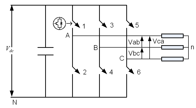
Figure 1. The power circuit of a three-phase VSI.
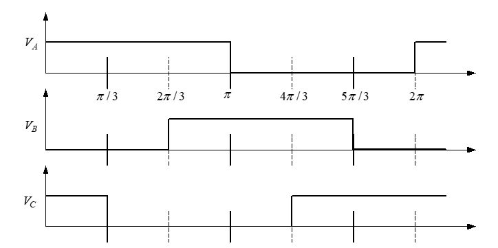
Figure 2. Leg voThe legge waveform of a three-phase VSI.
It is observed from Fig. 2. that one inverter leg's state changes after an interval of 60° and their state remains constant for 60° interval. Thus it follows that the leg voltages will have six distinct and discrete values in one cycle (360°).
Space vector representation of the three-phase inverter output voltages is introduced next. Space vector is defined as;
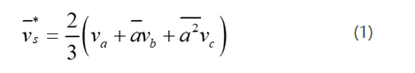
where ![]() . The space vector is a simultaneous representation of all the three-phase quantities. It is a complex variable and is function of time in contrast to the phasors.
. The space vector is a simultaneous representation of all the three-phase quantities. It is a complex variable and is function of time in contrast to the phasors.
Phase-to-neutral voltages of a star-connected load are most easily found by defining a voltage difference between the star point n of the load and the negative rail of the dc bus N. The following correlation then holds true:
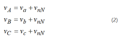
Since the phase voltages in a start connected load sum to zero, the summation of equation (2) yields
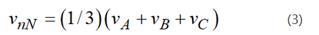
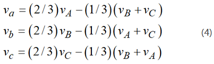
Substitution of (3) into (2) yields phase-to-neutral voltages of the load in the following form:
Phase voltages are summarised in Table 1 and their corresponding space vectors are listed in Table 2.
Table 1. Phase voltage values for different switching states.
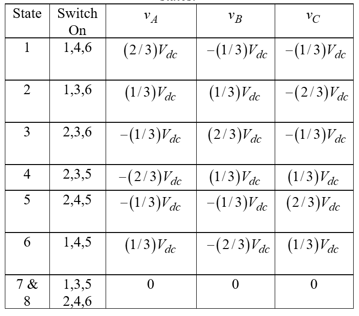
Table 2. Phase voltage space vectors.
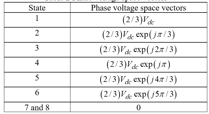
The discrete phase voltage space vector positions are shown in Fig. 3.
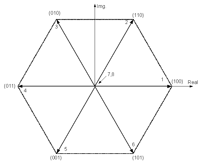
Figure 3. Phase voltage space vectors.
The binary numbers on the figure indicate the switch state of inverter legs. Here 1 implies upper switch being on and 0 refers to the lower switch of the leg being on. The most significant bit is for leg A, the least significant bit is related to leg C and the middle is for leg B.
3. SPACEpace VECTOR PULSE WIDTH MODULATIONector Pulse Width Modulation (SVPMW)
This section briefly discusses the space vector PWM principle. This PWM method is frequently used in vector controlled and direct torque controlled drives. In vector controlled drive this technique is used for reference voltage generation when current control is exercised in rotating reference frame.
It is seen in the previous section that a three-phase VSI generates eight switching states which include six active and two zero states. These vectors form a hexagon (Fig. 3) which can be seen as consisting of six sectors spanning 60° each. The reference vector which represents three-phase sinusoidal voltage is generated using SVPWM by switching between two nearest active vectors and zero vector. To calculate the time of application of different vectors, consider Fig. 4, depicting the position of differently available space vectors and the reference vector in the first sector.
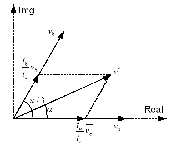
Figure 4. The principle of space vector time calculation.
The time of application of active space voltage vectors is found from Fig. 4 as;
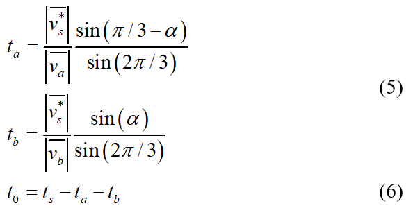
Where ![]()
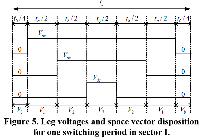
In order to obtain fixed switching frequency and optimum harmonic performance from SVPWM, each leg should change its sate only once in one switching period. This is achieved by applying zero state vector followed by two adjacent active state vector in half switching period. The next half of the switching period is the mirror image of the first half. The total switching period is divided intro 7 parts, the zero vector is applied for 1/4th of the total zero vector time first followed by the application of active vectors for half of their application time and then again zero vector is applied for 1/4th of the zero vector time. This is then repeated in the next half of the switching period. This is how symmetrical SVPWM is obtained. The leg voltage in one switching period is depicted in Fig. 5 for sector I.
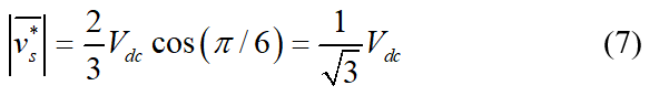
The sinusoidal reference space vector form a circular trajectory inside the hexagon. The largest output voltage magnitude that can be achieved using SVPWM is the radius of the largest circle that can be inscribed within the hexagon. This circle is tangential to the mid points of the lines joining the ends of the active space vector. Thus the maximum obtainable fundamental output voltage is;
4. MATLABatlab/SIMULINK MODELimulink Model
This section details the step by step development of Matlab/Simulink model for SVPWM. The Simulink model is shown in Fig. 6. Each block is further elaborated in Fig. 7. The Matlab code used to generate the switching pattern is also provided. Each sub-blocks of Fig. 6 is described in the following sub-section.
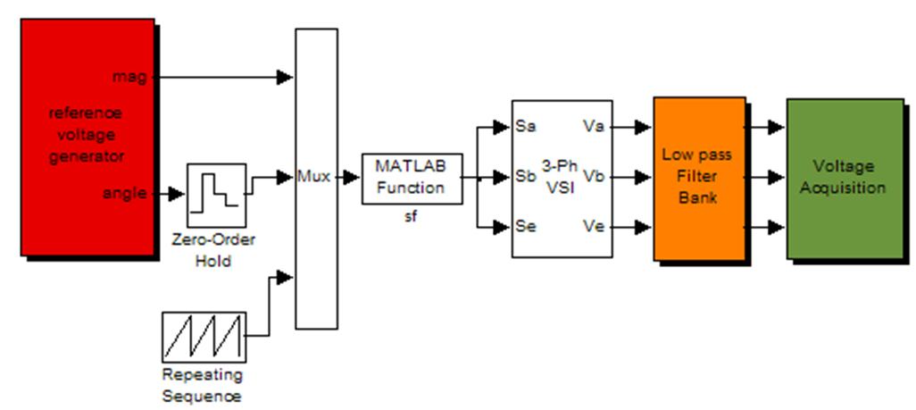
Figure 6. Matlab/Simulink Model of SVPWM.
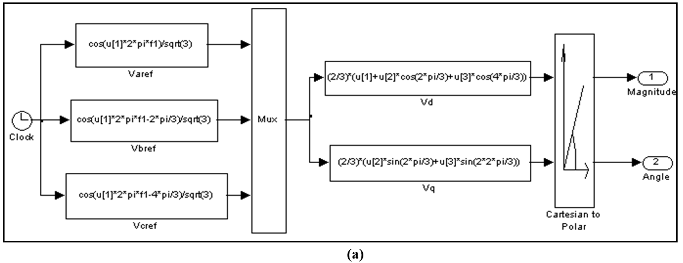
Figure 7. Sub-blocks of Matlab/Simulink model: (a) Reference voltage generation (b) VSI (c) Filters
4.1. Reference Voltage Generation Block
Three-phase sinusoidal voltage is generated using 'function' block from 'Functions & Tables' sub-library of Simulink. This is then converted into two-phase equivalent using Clark's transformation equations [1]. This is once again implemented using the 'function' blocks. Further, the two-phase equivalent is transformed to polar form using 'Cartesian to polar' block from 'Simulink extras' sub-library. The output of this block is the magnitude of the reference as the first output and the corresponding angle of the reference as the second output.
4.2. Switching Time Calculation
The switching time and corresponding switch state for each power switch are calculated in Matlab function block 'sf' using expressions (5) and (6). The Matlab code requires the magnitude of the reference, the angle of the reference and timer signal for comparison. The angle of the reference voltage is held for each switching period so that its value does not change during time calculation. The angle information is used for sector identification in Matlab code 'aaa'. Further, a ramping time signal is generated to be used in Matlab code. This ramp is generated using 'repeating sequence' from the source sub-library.
The Matlab code firstly identifies the sector of the reference voltage. The time of application of active and zero vectors are then calculated. The times are then arranged according to Fig. 5. This time is then compared with the ramp timer signal. Depending upon the location of the time signal, the switch state is defined. This switch state is then passed on to the inverter block.
4.3. Three-phase Inverter Block
The inverter model is build using 'function' blocks according to the expression (4). Thus the output of the inverter block is the phase voltages.
4.4. Filter Blocks
The PWM voltage signal is filtered using the first order filter. This is implemented using 'Transfer function' block from 'Continuous' sub-library. The time constant of the first-order filter is chosen as 0.8ms.
4.5. Voltage Acquisition
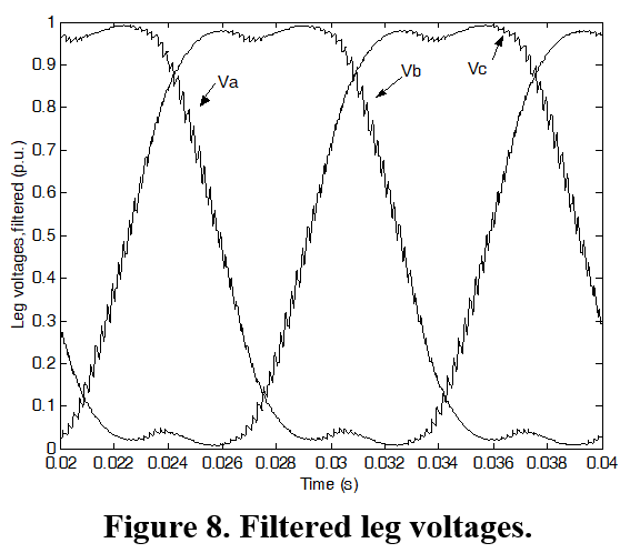
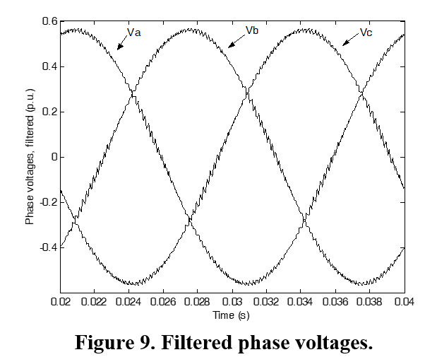
The filtered phase voltages are stored in workspaces in this block.
Simulation is carried out using the developed model for maximum obtainable reference voltage and the resulting filtered leg and phase voltages are shown in Figs. 8 and 9.
5. CONCLUSIONSonclusions
A simple Matlab/Simulink model is presented to implement SVPWM for three-phase VSI. A brief review of the VSI model is also reported based on space vector representation. A Matlab/Simulink based model for implementation of SVPWM is presented. The step-by-step model development is reported. The presented model gives an insight into the SVPWM. By varying the magnitude of the input reference different modulation index can be achieved [3].
References
- Holmes, G.D. and Lipo, T.A., Pulse Width Modulation for Power Converters - Principles and Practice, IEEE Press Series on Power Eng., John Wiley and Sons, Piscataway, NJ, USA, 2003.
- Kazmierkowski, M.P., Krishnan, R. and Blaabjerg, F., Control in power electronics- selected problems, Academic Press, California, USA, 2002.
- A. Iqbal, A. Lamine, I. Ashraf and Mohibullah, "MATLAB/SIMULINK MODEL OF SPACE VECTOR PWM FOR THREE-PHASE VOLTAGE SOURCE INVERTER", Proc. IEEE UPEC 2006.