The concept of photonic crystals was proposed in 1987. Afterward, this kind of artificial structure with photonic bandgaps attracted much attention for their special dispersion. Such artificial structures fabricated at the micro- or nanoscale, namely photonic crystals, can use the periodical changes of material refractive index to affect the propagation of a light beam, imitating natural crystals that give rise to the X-ray diffraction with their atomic lattices. Thus, with this kind of artificial structure, photonic crystals can pave prospective ways for specific light modulation with ultracompact form factors.
Auspiciously, thanks to the monolithic integration of photonic crystals embedded in the epitaxial structures, a rerevolutionary semiconductor laser technology nowadays turns over a new leaf. With the monolithic integration, a , namely the photonic crystal can be adopted as a lateral laser cavity, generating a photonicc-crystal surface-emitting laser (PCSEL) [14,15]. Through th, e band-edge resonance of embedded photonic crystal, laser light emission from aerges. PCSEL exhibits a high-power single-mode operation with controllability. Moreover, such a laser light emission presents a snot only a symmetric beam profile with narrow beam divergence and spectral width [16,17]. Altbut also a high-power ogpether, PCSEL is quite suitable for the LiDAR application, enabling a lens-free and adjustment-free apparatus [18–20]ration with controllability. Therefore, it may be the holy grail for an ultracompact time-of-flight (ToF) LiDAR system.
- photonic-crystal surface-emitting laser
- PCSEL
- light detection and ranging
- LiDAR
1. Introduction
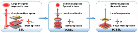
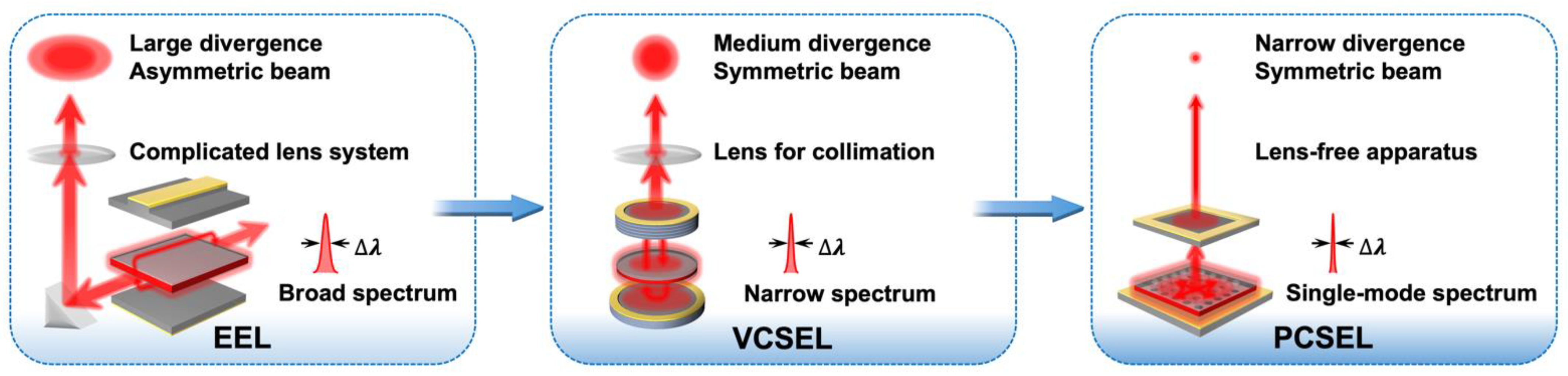
Figure 1.
Schematic illustration for the development progress of laser light sources.
2. Operation Principle
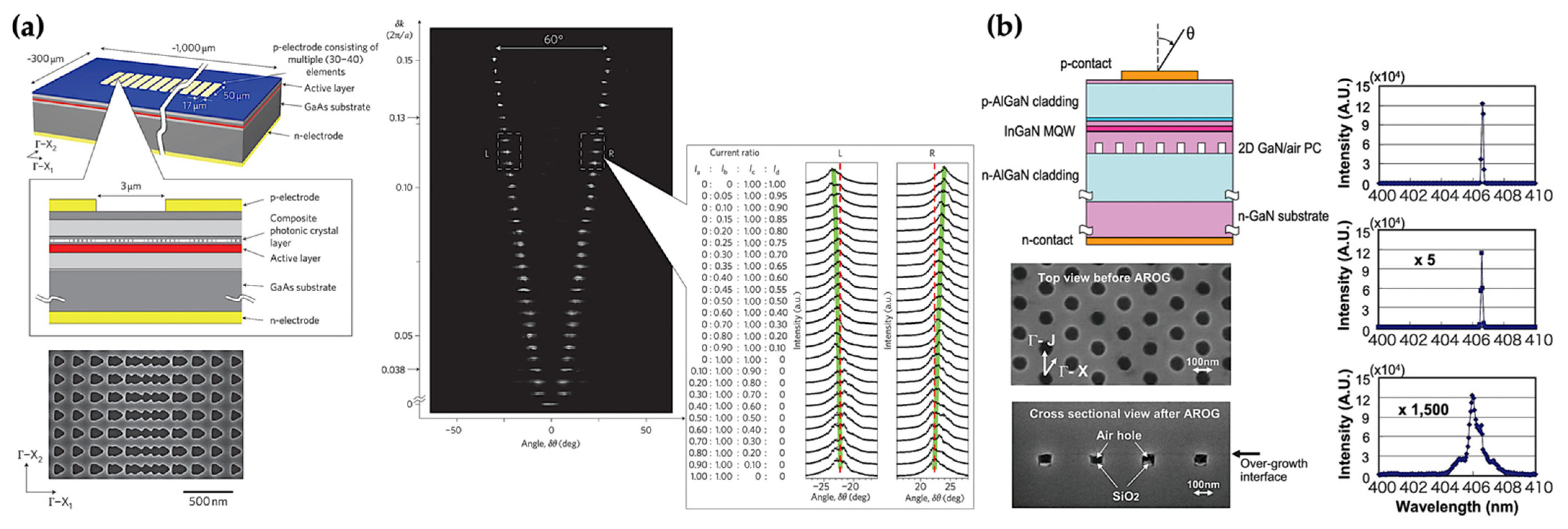
3. Light-Emitting Control and Emission Wavelength Expansion
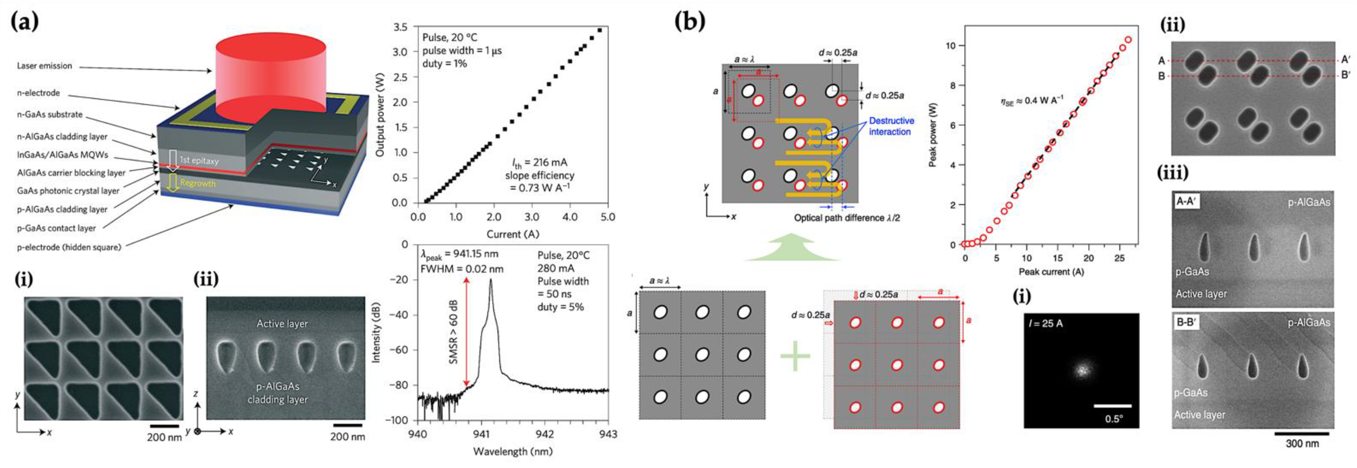
4. High-Power Operation with the Concept of Double-Lattice Structure
5. Toward a Lens-Free and Adjustment-Free ToF LiDAR System
As the tendency of miniaturization in relevant optical technologies, ultracompact optical devices with miscellaneous functionalities are urgently needed. With the state-of-the-art progress in PCSELs, such laser devices can provide higher-power and extraordinarily narrow-divergence laser light beams while keeping a symmetric beam profile. Therefore, based on these laser devices, prospects to ameliorate the bulky form factor of common optical devices are in demand.Owing to the blossom of advancements for autonomous vehicles, i.e., self-driving cars, depth perception, and LiDAR applications are flourishing. In addition, for a ToF LiDAR system, PCSELs can be appropriate laser light sources as well. In 2021, M. Yoshida et al. proposed a 10-watt-class PCSEL with DBR, operating in pulsed mode with the repetition rate and corresponding pulse width of 1 kHz and 100 ns, respectively [85]. Moreover, in 2021, R. Morita et al. introduced the design of two-dimensionally arranged gain and loss sections, and the corresponding operation in pulsed mode can even reach astonishing results [86]. In such a well-designed PCSEL, a relevant peak power of 20 W can be achieved with the repetition rate and corresponding pulse width of 1 GHz and 35 ps, respectively.
Owing to the blossom of advancements for autonomous vehicles, i.e., self-driving cars, depth perception, and LiDAR applications are flourishing. In addition, for a ToF LiDAR system, PCSELs can be appropriate laser light sources as well. In 2021, M. Yoshida et al. proposed a 10-watt-class PCSEL with DBR, operating in pulsed mode with the repetition rate and corresponding pulse width of 1 kHz and 100 ns, respectively [70]. Moreover, in 2021, R. Morita et al. introduced the design of two-dimensionally arranged gain and loss sections, and the corresponding operation in pulsed mode can even reach astonishing results [71]. In such a well-designed PCSEL, a relevant peak power of 20 W can be achieved with the repetition rate and corresponding pulse width of 1 GHz and 35 ps, respectively.Additionally, the performance trade-offs of PCSEL technology emerge with several challenges in power scaling, modal competition, charge injection control, etc. Auspiciously, with abundant efforts, these challenges can be ameliorated and conquered [15]. For real-world applications, the thermal characteristics and relevant management of laser devices are crucial and should be concerned as well [87–92]. In 2020, M. De Zoysa et al. conducted the relevant thermal analysis for PCSELs under continuous wave (CW) operation with heat dissipation [92]. The corresponding temperature properties for an assembled double-lattice PCSEL in a water-cooling package with a highly thermally conductive sub-mount are investigated, providing a practical paradigm for high-power operation. Nowadays, artificial intelligence-assisted technology can be even adopted for the fabrication as well [93]. Thus, as shown in Figure 9, these demonstrated paradigms can promise pavements toward a lens-free and adjustment-free ultracompact ToF LiDAR system soon.
Additionally, the performance trade-offs of PCSEL technology emerge with several challenges in power scaling, modal competition, charge injection control, etc. Auspiciously, with abundant efforts, these challenges can be ameliorated and conquered [2]. For real-world applications, the thermal characteristics and relevant management of laser devices are crucial and should be concerned as well [72][73][74][75][76][77]. In 2020, M. De Zoysa et al. conducted the relevant thermal analysis for PCSELs under continuous wave (CW) operation with heat dissipation [77]. The corresponding temperature properties for an assembled double-lattice PCSEL in a water-cooling package with a highly thermally conductive sub-mount are investigated, providing a practical paradigm for high-power operation. Nowadays, artificial intelligence-assisted technology can be even adopted for the fabrication as well [78]. Thus, as shown in Figure 6, these demonstrated paradigms can promise pavements toward a lens-free and adjustment-free ultracompact ToF LiDAR system soon.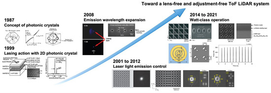
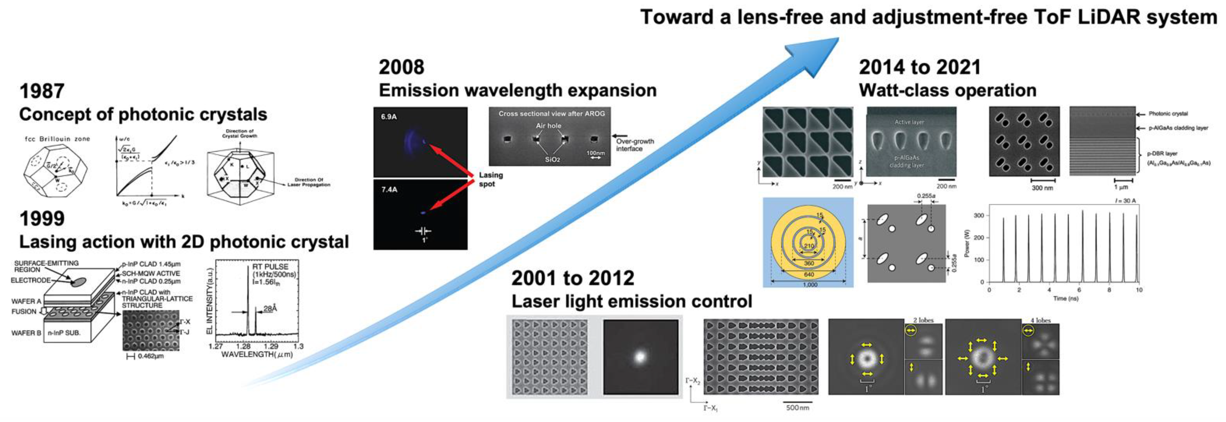
Figure 96. Development progress of PCSEL technology toward an ultracompact ToF LiDAR system [21,22,33,34,45,52,54,55,66,77,86].
References
- Ishizaki, K.; De Zoysa, M.; Noda, S. Progress in photonic-crystal surface-emitting lasers. Photonics 2019, 6, 96.
- Kalapala, A.; Song, A.; Pan, M.; Gautam, C.; Overman, L.; Reilly, K.; Rotter, T.; Balakrishnan, G.; Gibson, R.; Bedford, R.; et al. Scaling challenges in high power photonic crystal surface-emitting lasers. IEEE J. Quantum Electron. 2022.
- Wang, Z.; Tong, C.; Wang, L.; Lu, H.; Tian, S.; Wang, L. Photonic crystal surface emitting laser operating in pulse-periodic regime with ultralow divergence angle. Photonics 2021, 8, 323.
- Taylor, R.J.; Childs, D.; Hogg, R. Vector photonics: The commercial journey of PCSELs and their pathway to high power. In Proceedings of the SPIE High-Power Diode Laser Technology XX, San Francisco, CA, USA, 22 January–28 February 2022; Volume PC1198304.
- de Zoysa, M.; Inoue, T.; Yoshida, M.; Ishizaki, K.; Kunishi, W.; Gelleta, J.; Noda, S. Light detection functionality of photonic-crystal lasers. IEEE J. Quantum Electron. 2021, 57, 6400208.
- Noda, S. Progress of photonic crystal surface-emitting lasers: Paradigm shift for lidar sensing and laser processing. In Proceedings of the Laser Resonators, Microresonators, and Beam Control XXIII, Virtual, 6–12 March 2021; Volume 11672, p. 1167203.
- Noda, S. Photonic crystal surface-emitting lasers and their application to lidar. In Proceedings of the 2021 26th Microoptics Conference (MOC), Hamamatsu, Japan, 26–29 September 2021; pp. 1–2.
- Yablonovitch, E. Inhibited spontaneous emission in solid-state physics and electronics. Phys. Rev. Lett. 1987, 58, 2059.
- John, S. Strong localization of photons in certain disordered dielectric superlattices. Phys. Rev. Lett. 1987, 58, 2486.
- Purcell, E.M. Spontaneous emission probabilities at radio frequencies. Phys. Rev. 1946, 69, 681.
- Heinzen, D.J.; Childs, J.J.; Thomas, J.E.; Feld, M.S. Enhanced and inhibited visible spontaneous emission by atoms in a confocal resonator. Phys. Rev. Lett. 1987, 58, 1320.
- Hirayama, H.; Hamano, T.; Aoyagi, Y. Novel surface emitting laser diode using photonic band-gap crystal cavity. Appl. Phys. Lett. 1996, 69, 791–793.
- Tandaechanurat, A.; Ishida, S.; Guimard, D.; Nomura, M.; Iwamoto, S.; Arakawa, Y. Lasing oscillation in a three-dimensional photonic crystal nanocavity with a complete bandgap. Nat. Photonics 2011, 5, 91–94.
- Ryu, H.Y.; Notomi, M.; Lee, Y.H. High-quality-factor and small-mode-volume hexapole modes in photonic-crystal-slab nanocavities. Appl. Phys. Lett. 2003, 83, 4294–4296.
- Takano, H.; Akahane, Y.; Asano, T.; Noda, S. In-plane-type channel drop filter in a two-dimensional photonic crystal slab. Appl. Phys. Lett. 2004, 84, 2226–2228.
- Sugitatsu, A.; Asano, T.; Noda, S. Line-defect–waveguide laser integrated with a point defect in a two-dimensional photonic crystal slab. Appl. Phys. Lett. 2005, 86, 171106.
- Nozaki, K.; Kita, S.; Baba, T. Room temperature continuous wave operation and controlled spontaneous emission in ultrasmall photonic crystal nanolaser. Opt. Express 2007, 15, 7506–7514.
- Imada, M.; Noda, S.; Chutinan, A.; Tokuda, T.; Murata, M.; Sasaki, G. Coherent two-dimensional lasing action in surface-emitting laser with triangular-lattice photonic crystal structure. Appl. Phys. Lett. 1999, 75, 316–318.
- Meier, M.; Mekis, A.; Dodabalapur, A.; Timko, A.; Slusher, R.E.; Joannopoulos, J.D.; Nalamasu, O. Laser action from two-dimensional distributed feedback in photonic crystals. Appl. Phys. Lett. 1999, 74, 7–9.
- Imada, M.; Chutinan, A.; Noda, S.; Mochizuki, M. Multidirectionally distributed feedback photonic crystal lasers. Phys. Rev. B 2002, 65, 195306.
- Dems, M.; Kotynski, R.; Panajotov, K. Planewave admittance method—A novel approach for determining the electromagnetic modes in photonic structures. Opt. Express 2005, 13, 3196–3207.
- Drong, M.; Dems, M.; Perina, J.; Fordos, T.; Jaffres, H.Y.; Postava, K.; Drouhin, H.J. Time-dependent laser cavity perturbation theory: Exploring future nano-structured photonic devices in semi-analytic way. J. Lightwave Technol. 2022.
- Dems, M. Convergence analysis of various factorization rules in the Fourier-Bessel basis for solving Maxwell equations using modal methods. Opt. Express 2021, 29, 4378–4391.
- Frasunkiewicz, L.; Panajotov, K.; Thienpont, H.; Dems, M.; Czyszanowski, T. Transverse mode mixing in a coupled-cavity VCSEL. J. Lightwave Technol. 2020, 38, 5774–5782.
- Kuc, M.; Piskorski, Ł.; Dems, M.; Wasiak, M.; Sokół, A.K.; Sarzała, R.P.; Czyszanowski, T. Numerical investigation of the impact of ITO, AlInN, plasmonic GaN and top gold metalization on semipolar green EELs. Materials 2020, 13, 1444.
- Noda, S.; Kitamura, K.; Okino, T.; Yasuda, D.; Tanaka, Y. Photonic-crystal surface-emitting lasers: Review and introduction of modulated-photonic crystals. IEEE J. Sel. Top. Quantum Electron. 2017, 23, 1.
- Sakai, K.; Miyai, E.; Noda, S. Coupled-wave model for square-lattice two-dimensional photonic crystal with transverse-electric-like mode. Appl. Phys. Lett. 2006, 89, 021101.
- Sakai, K.; Miyai, E.; Noda, S. Coupled-wave theory for square-lattice photonic crystal lasers with TE polarization. IEEE J. Quantum Electron. 2010, 46, 788–795.
- Liang, Y.; Peng, C.; Sakai, K.; Iwahashi, S.; Noda, S. Three-dimensional coupled-wave model for square-lattice photonic crystal lasers with transverse electric polarization: A general approach. Phys. Rev. B 2011, 84, 195119.
- Yoshida, M.; De Zoysa, M.; Ishizaki, K.; Tanaka, Y.; Kawasaki, M.; Hatsuda, R.; Song, B.; Gelleta, J.; Noda, S. Double-lattice photonic-crystal resonators enabling high-brightness semiconductor lasers with symmetric narrow-divergence beams. Nat. Mater. 2019, 18, 121–128.
- Koba, M.; Szczepański, P. Analysis of mode competition in a 2-D square lattice photonic crystal laser with transverse magnetic polarization. IEEE J. Quantum Electron. 2015, 51, 1–13.
- Yang, Y.; Peng, C.; Liang, Y.; Li, Z.; Noda, S. Three-dimensional coupled-wave theory for the guided mode resonance in photonic crystal slabs: TM-like polarization. Opt. Lett. 2014, 39, 4498–4501.
- Yang, Y.; Peng, C.; Li, Z. Semi-analytical approach for guided mode resonance in high-index-contrast photonic crystal slab: TE polarization. Opt. Express 2013, 21, 20588–20600.
- Liang, Y.; Peng, C.; Ishizaki, K.; Iwahashi, S.; Sakai, K.; Tanaka, Y.; Kitamura, K.; Noda, S. Three-dimensional coupled-wave analysis for triangular-lattice photonic-crystal surface-emitting lasers with transverse-electric polarization. Opt. Express 2013, 21, 565–580.
- Noda, S.; Yokoyama, M.; Imada, M.; Chutinan, A.; Mochizuki, M. Polarization mode control of two-dimensional photonic crystal laser by unit cell structure design. Science 2001, 293, 1123–1125.
- Hong, Y.H.; Hsu, W.C.; Tsai, W.C.; Huang, Y.W.; Chen, S.C.; Kuo, H.C. Ultracompact nanophotonics: Light emission and manipulation with metasurfaces. Nanoscale Res. Lett. 2022, 17, 41.
- Miyai, E.; Sakai, K.; Okano, T.; Kunishi, W.; Ohnishi, D.; Noda, S. Lasers producing tailored beams. Nature 2006, 441, 946.
- Kitamura, K.; Nishimoto, M.; Sakai, K.; Noda, S. Needle-like focus generation by radially polarized halo beams emitted by photonic-crystal ring-cavity laser. Appl. Phys. Lett. 2012, 101, 221103.
- Iwahashi, S.; Kurosaka, Y.; Sakai, K.; Kitamura, K.; Takayama, N.; Noda, S. Higher-order vector beams produced by photonic-crystal lasers. Opt. Express 2011, 19, 11963–11968.
- Kurosaka, Y.; Iwahashi, S.; Liang, Y.; Sakai, K.; Miyai, E.; Kunishi, W.; Ohnishi, D.; Noda, S. On-chip beam-steering photonic-crystal lasers. Nat. Photonics 2010, 4, 447–450.
- Ohnishi, D.; Okano, T.; Imada, M.; Noda, S. Room temperature continuous wave operation of a surface-emitting two-dimensional photonic crystal diode laser. Opt. Express 2004, 12, 1562–1568.
- Kim, M.; Kim, C.S.; Bewley, W.W.; Lindle, J.R.; Canedy, C.L.; Vurgaftman, I.; Meyer, J.R. Surface-emitting photonic-crystal distributed-feedback laser for the midinfrared. Appl. Phys. Lett. 2006, 88, 191105.
- Johnson, M.T.; Siriani, D.F.; Peun, T.M.; Choquette, K.D. Beam steering via resonance detuning in coherently coupled vertical cavity laser arrays. Appl. Phys. Lett. 2013, 103, 201115.
- Siriani, D.F.; Choquette, K.D. Implant defined anti-guided vertical-cavity surface-emitting laser arrays. IEEE J. Quantum Electron. 2011, 47, 160–164.
- Alias, M.S.; Shaari, S.; Leisher, P.O.; Choquette, K.D. Single transverse mode control of VCSEL by photonic crystal and trench patterning. Photonics Nanostructures Fundam. Appl. 2010, 8, 38–46.
- Siriani, D.F.; Choquette, K.D. Electronically controlled two-dimensional steering of in-phase coherently coupled vertical-cavity laser arrays. IEEE Photonics Technol. Lett. 2010, 23, 167–169.
- Gao, Z.; Thompson, B.J.; Dave, H.; Fryslie, S.T.; Choquette, K.D. Non-hermiticity and exceptional points in coherently coupled vertical cavity laser diode arrays. Appl. Phys. Lett. 2019, 114, 061103.
- Kominis, Y.; Choquette, K.D.; Bountis, A.; Kovanis, V. Exceptional points in two dissimilar coupled diode lasers. Appl. Phys. Lett. 2018, 113, 081103.
- Thompson, B.J.; Gao, Z.; Fryslie, S.T.; Choquette, K.D. Mode engineering in linear coherently coupled vertical-cavity surface-emitting laser arrays. IEEE J. Sel. Top. Quantum Electron. 2019, 25, 1701205.
- Dave, H.; Gao, Z.; Fryslie, S.T.M.; Thompson, B.J.; Choquette, K.D. Static and dynamic properties of coherently-coupled photonic-crystal vertical-cavity surface-emitting laser arrays. IEEE J. Sel. Top. Quantum Electron. 2019, 25, 1700208.
- Matsubara, H.; Yoshimoto, S.; Saito, H.; Jianglin, Y.; Tanaka, Y.; Noda, S. GaN photonic-crystal surface-emitting laser at blue-violet wavelengths. Science 2008, 319, 445–447.
- Lu, T.C.; Chen, S.W.; Kao, T.T.; Liu, T.W. Characteristics of GaN-based photonic crystal surface emitting lasers. Appl. Phys. Lett. 2008, 93, 111111.
- Bin, J.; Feng, K.; Shen, W.; Meng, M.; Liu, Q. Investigation on GaN-based membrane photonic crystal surface emitting lasers. Materials 2022, 15, 1479.
- Choi, Y.S.; Hennessy, K.; Sharma, R.; Haberer, E.; Gao, Y.; DenBaars, S.P.; Nakamura, S.; Meier, C. GaN blue photonic crystal membrane nanocavities. Appl. Phys. Lett. 2005, 87, 243101.
- David, A.; Fujii, T.; Moran, B.; Nakamura, S.; DenBaars, S.P.; Weisbuch, C.; Benisty, H. Photonic crystal laser lift-off GaN light-emitting diodes. Appl. Phys. Lett. 2006, 88, 133514.
- Hong, K.B.; Chen, L.R.; Huang, K.C.; Yen, H.T.; Weng, W.C.; Chuang, B.H.; Lu, T.C. Impact of air-hole on the optical performances of epitaxially regrown p-side up photonic crystal surface-emitting lasers. IEEE J. Sel. Top. Quantum Electron. 2021, 28, 9479706.
- Reuterskiöld Hedlund, C.; Martins De Pina, J.; Kalapala, A.; Liu, Z.; Zhou, W.; Hammar, M. Buried InP/air hole photonic-crystal surface-emitting lasers. Phys. Status Solidi A 2021, 218, 2000416.
- McKenzie, A.F.; King, B.C.; Rae, K.J.; Thoms, S.; Gerrard, N.D.; Orchard, J.R.; Nishi, K.; Takemasa, K.; Sugawara, M.; Taylor, R.J.E.; et al. Void engineering in epitaxially regrown GaAs-based photonic crystal surface emitting lasers by grating profile design. Appl. Phys. Lett. 2021, 118, 021109.
- Huang, Y.H.; Yang, Z.X.; Cheng, S.L.; Lin, C.H.; Lin, G.; Sun, K.W.; Lee, C.P. Effect of hole shift on threshold characteristics of gasb-based double-hole photonic-crystal surface-emitting lasers. Micromachines 2021, 12, 468.
- Bian, Z.; Rae, K.J.; King, B.C.; Kim, D.; Li, G.; Thoms, S.; Childs, D.T.D.; Gerrard, N.D.; Babazadeh, N.; Reynolds, P.; et al. Comparative analysis of void-containing and all-semiconductor 1.5 µm InP-based photonic crystal surface-emitting laser diodes. AIP Adv. 2021, 11, 065315.
- Chen, L.R.; Hong, K.B.; Huang, K.C.; Liu, C.L.; Lin, W.; Lu, T.C. Study of an epitaxial regrowth process by MOCVD for photonic-crystal surface-emitting lasers. Cryst. Growth Des. 2021, 21, 3521–3527.
- Hirose, K.; Liang, Y.; Kurosaka, Y.; Watanabe, A.; Sugiyama, T.; Noda, S. Watt-class high-power, high-beam-quality photonic-crystal lasers. Nat. Photonics 2014, 8, 406–411.
- Williams, D.M.; Groom, K.M.; Stevens, B.J.; Childs, D.T.; Taylor, R.J.; Khamas, S.; Hogg, R.A.; Ikeda, N.; Sugimoto, Y. Epitaxially regrown GaAs-based photonic crystal surface-emitting laser. IEEE Photonics Technol. Lett. 2012, 24, 966–968.
- Hamamatsu Photonics, Photonic Crystal Surface Emitting Laser diodes (PCSEL). Available online: https://www.hamamatsu.com/jp/en.html (accessed on 23 April 2022).
- Inoue, T.; Morita, R.; Yoshida, M.; De Zoysa, M.; Tanaka, Y.; Noda, S. Comprehensive analysis of photonic-crystal surface-emitting lasers via time-dependent three-dimensional coupled-wave theory. Phys. Rev. B 2019, 99, 035308.
- De Zoysa, M.; Yoshida, M.; Ishizaki, K.; Song, B.S.; Tanaka, Y.; Hatsuda, R.; Fukuhara, S.; Noda, S. 7W CW Operation of double-lattice photonic-crystal lasers. In Proceedings of the 2018 IEEE International Semiconductor Laser Conference (ISLC), Santa Fe, NM, USA, 16–19 September 2018; pp. 1–2.
- Iadanza, S.; Liles, A.A.; Butler, S.M.; Hegarty, S.P.; O’Faolain, L. Photonic crystal lasers: From photonic crystal surface emitting lasers (PCSELs) to hybrid external cavity lasers (HECLs) and topological PhC lasers. Opt. Mater. Express 2021, 11, 3245–3274.
- Gao, X.; Yang, L.; Lin, H.; Zhang, L.; Li, J.; Bo, F.; Wang, Z.; Lu, L. Dirac-vortex topological cavities. Nat. Nanotechnol. 2020, 15, 1012–1018.
- Wang, Z.; Liang, Y.; Beck, M.; Scalari, G.; Faist, J. Topological charge of finite-size photonic crystal modes. Phys. Rev. B 2020, 102, 045122.
- Yoshida, M.; De Zoysa, M.; Ishizaki, K.; Kunishi, W.; Inoue, T.; Izumi, K.; Hatsuda, R.; Noda, S. Photonic-crystal lasers with high-quality narrow-divergence symmetric beams and their application to LiDAR. J. Phys. Photonics 2021, 3, 022006.
- Morita, R.; Inoue, T.; De Zoysa, M.; Ishizaki, K.; Noda, S. Photonic-crystal lasers with two-dimensionally arranged gain and loss sections for high-peak-power short-pulse operation. Nat. Photonics 2021, 15, 311–318.
- Takagi, S.; Tanimura, H.; Kakuno, T.; Hashimoto, R.; Kaneko, K.; Saito, S. Evaluation of thermal resistance of surface-emitting quantum cascade laser using structural function and 3D thermal flow simulation. In Proceedings of the 9th International Conference on Photonics, Optics and Laser Technology (PHOTOPTICS 2021), Online Streaming, 11–13 February 2021; pp. 88–93.
- Guo, X.; Wang, Y.; Qi, A.; Qi, F.; Zhang, S.; Zheng, W. Photonic crystal surface emitting laser with ultralow thermal resistance and narrow divergence angle. In Proceedings of the 2016 Conference on Lasers and Electro-Optics (CLEO), San Jose, CA, USA, 5–10 June 2016.
- Sciancalepore, C.; Bakir, B.B.; Seassal, C.; Letartre, X.; Harduin, J.; Olivier, N.; Fedeli, J.M.; Viktorovitch, P. Thermal, modal, and polarization features of double photonic crystal vertical-cavity surface-emitting lasers. IEEE Photonics J. 2012, 4, 399–410.
- Haghighat, G.; Ahmadi, V. Analysis of SHB and thermal characteristics in PC-VCSEL considering photonic crystal parameters. In Proceedings of the OSA Asia Communications and Photonics Conference, Shanghai, China, 13–16 November 2011; Volume 83082G.
- Czyszanowski, T. Thermal properties and wavelength analysis of telecom oriented photonic-crystal VCSELs. Opto-electron. Rev. 2010, 18, 56–62.
- De Zoysa, M.; Yoshida, M.; Song, B.; Ishizaki, K.; Inoue, T.; Katsuno, S.; Izumi, K.; Tanaka, Y.; Hatsuda, R.; Gelleta, J.; et al. Thermal management for CW operation of large-area double-lattice photonic-crystal lasers. JOSA B 2020, 37, 3882–3887.
- Noda, S.; Yoshida, M.; Kunishi, W.; Inoue, T.; Ishizaki, K.; De Zoysa, M.; Kitamura, K.; Shimaji, N.; Nishimura, K. Photonic crystal lasers: Fabrication with AI-assisted technology and application to LiDAR system. AI Opt. Data Sci. II SPIE 2021, 11703, 117030M.