The concept of photonic crystals was proposed in 1987. Afterward, this kind of artificial structure with photonic bandgaps attracted much attention for their special dispersion. Such artificial structures fabricated at the micro- or nanoscale, namely photonic crystals, can use the periodical changes of material refractive index to affect the propagation of a light beam, imitating natural crystals that give rise to the X-ray diffraction with their atomic lattices. Thus, with this kind of artificial structure, photonic crystals can pave prospective ways for specific light modulation with ultracompact form factors.
Auspiciously, Athanks to the monolithic integration of photonic crystals embedded in the epitaxial structures, a revolutionary semiconductor laser technology, namely the nowadays turns over a new leaf. With the monolithic integration, a photonic crystal can be adopted as a lateral laser cavity, generating a photonic-crystal surface-emitting laser (PCSEL), [14,15]. Through the band-edge resonance of emberges.dded photonic crystal, laser light emission from a PCSEL exhibits not only a sa high-power single-mode operation with controllability. Moreover, such a laser light emission presents a symmetric beam profile with narrow beam divergence but also aand spectral width [16,17]. hiAltogh-power operation with controllabilityether, PCSEL is quite suitable for the LiDAR application, enabling a lens-free and adjustment-free apparatus [18–20]. Therefore, it may be the holy grail for an ultracompact time-of-flight (ToF) LiDAR system.
1. Introduction
Auspiciously, thanks to the monolithic integration of photonic crystals embedded in the epitaxial structures, a revolutionary semiconductor laser technology nowadays turns over a new leaf. With the monolithic integration, a photonic crystal can be adopted as a lateral laser cavity, generating a photonic-crystal surface-emitting laser (PCSEL) [1][2]. T
hrough
the band-edge resonance of embedded photonic crystal, laser light emission from a PCSEL exhibits a high-power single-mode operation with controllability. Moreover, such a laser light emission presents a symmetric beam profile with narrow beam divergence and spectral width [3][4]. Alte concept of pho
get
her, PCSEL is quite suitable for the LiDAR application, enabling a lens-free and adjustment-free apparatus [5][6][7].
The onic
oncept of photonic ccrystals was independently proposed by E. Yablonovitch and S. John in 1987
[8][9][21,22]. Afterward, this kind of artificial structure with photonic bandgaps attracted much attention for their special dispersion. As an analogy to the quantum mechanics of electrons in a natural crystal, a photonic crystal uses the periodical changes in the refractive index of composed dielectric materials as an artificial crystal, and thus exhibits a photonic band structure. As a result, for such a photonic band structure, a photonic bandgap exists in between these bands, like the semiconductor bandgap in solid-state physics.
Accordingly, within these bands, the transmission of light beams is strictly inhibited, hence forming the forbidden bands. In early 1946, the enhancement effect for the spontaneous emission rate of a quantum system can be achieved by its environment, such as by exploiting a microcavity
[10][25]. Thereafter, relevant discussion on the coupling between electromagnetic fields and materials is well known as the Purcell effect, named after E. M. Purcell. Taking advantage of these bands for light inhibition, an engineered cavity with the reduction of corresponding mode volume can be accomplished; therefore, a bandgap type of photonic crystal for lasing is possible. Due to the volume reduction of such engineered micro- or nanocavity, the eventual number of modes supported by the bandgap type of photonic crystals can be decreased, resulting in a dramatically increased spontaneous emission coupling coefficient
[11][26]. Thus, in 1996, relevant lasing actions in such bandgap types of photonic crystals can be observed with an ultra-low lasing threshold, even theoretically achieving thresholdless lasers
[12][13][27,28]. Additionally, with pioneering effects utilizing the bandgap property of such photonic crystals, many significant applications and relevant optical manipulation can be realized, which are particularly important for the on-demand integration of on-chip light sources
[14][15][16][17][29,30,31,32].
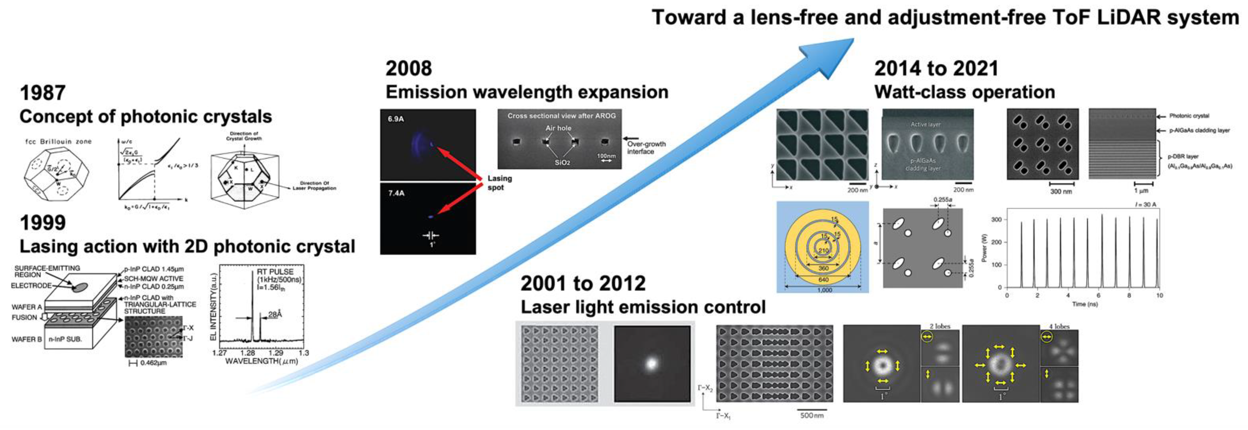
On the other hand, due to the formation of standing waves with zero group velocity of light at the band edges in such a photonic band structure, the resonant effect can also be exploited to achieve a large-area coherent resonance for lasing action, enabling a higher power operation while keeping the symmetric beam profile with narrow beam divergence and spectral width. For laser light sources toward the ultracompact ToF LiDAR system, schematic illustration of various laser modules and relevant development progress, are shown in Figure 1.
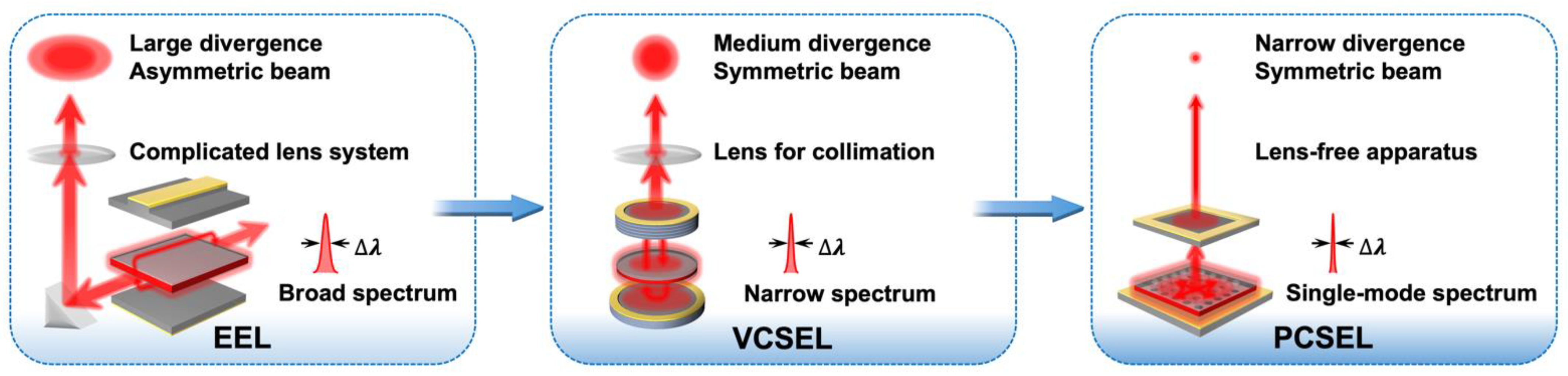
Figure 1.
Schematic illustration for the development progress of laser light sources.
2. Operation Principle
The exploitation of band-edge resonance can give rise to a large-area coherent resonance for lasing action; hence, a two-dimensional photonic crystal can be adopted as a laser cavity, generating a lateral cavity photonic-crystal surface-emitting laser. Accordingly, in 1999, two groups independently proposed this concept for the semiconductor lasers embedded with two-dimensional photonic crystals as laser cavities
[18][19][33,34]. As shown in
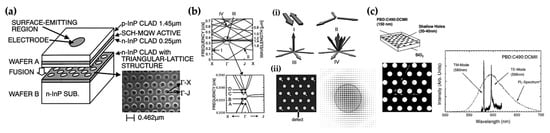
Figure 25a, M. Imada et al. presented a laser device with a triangular-lattice photonic crystal via bonding fabrication
[18][33]. In the proposed structure, a
p-InP cladding layer and InGaAsP multiple-quantum-well (MQW) layers serve as an active layer, namely the upper wafer A. For another wafer, namely the bottom wafer B, an
n-InP cladding layer is patterned with a triangular-lattice photonic crystal. Finally, via the wafer fusion technique, a bonded PCSEL device can be fabricated, thus embedding the photonic crystal near the active layer. For such a structure, light emission from the active layer is thereby guided by the
p- and
n-cladding layers, videlicet the adjoined photonic crystal, thus achieving a lasing action.
Figure 25. (
a) Schematic illustration of the surface-emitting laser embedded with a 2D triangular-lattice structure via wafer fusion technique
[18][33]. (
b) Band diagram of a 2D photonic crystal
[20][35].
Insets: (
i) Schematic illustration for the propagating directions of coupled waves at points I–IV. (
ii) Schematic illustration of defects introduced into a 2D photonic crystal. The corresponding electric field pattern can be calculated via finite-difference time-domain (FDTD) method. (
c) Schematic illustration of layer structure with a two-dimensional triangular lattice and the corresponding emission spectra from the device
[19][34]. Two lasing peaks with different polarizations can be observed. In addition, the spontaneous emission spectrum from the gain medium is shown with a dashed line.
In 2002, relevant lasing modes in a two-dimensional photonic crystal were theoretically and experimentally investigated with an in-plane multidirectional distributed feedback effect, as shown in
Figure 25b
[20][35]. Output laser light beam can be manipulated and coupled into specific directions. Moreover, a photonic-crystal laser device adopted with the band-edge mode at Γ-point enables specific radiation in a surface normal direction. Thus, an optimal band edge is figured out for a surface emission laser with truly coherent two-dimensional resonance.
It is worth mentioning that the exploitation of band-edge resonance in a triangular-lattice photonic crystal for lasing action is also demonstrated by M. Meier et al. in 1999, as shown in
Figure 25c
[19][34]. However, they did not conduct a further investigation for the achievement of coherent two-dimensional resonance. Multidirectional light propagation is not coupled to the in-plane photonic-crystal lattice structure, and thus two lasing peaks with different polarizations can be observed. A fast and accurate computational technique, namely the plane wave admittance method, for determining the electromagnetic modes in photonic structures was proposed by M. Dems et al. in 2005 as well
[21][36]. Thereupon, several remarkable efforts, especially for the relevant numerical simulation, are established by M. Dems’s group, making great contributions to modeling activities
[21][22][23][24][25][36,37,38,39,40].
3. Light-Emitting Control and Emission Wavelength Expansion
For the betterment of laser light emission, namely toward a high-power single-mode operation with controllability, relevant research of PCSELs was thereafter shifted to the photonic crystals with square-lattice structure. For such a square-lattice structure, the corresponding four fundamental Bloch waves, oscillating in transverse-electric (TE) polarization, cannot be directly coupled, yet the use of higher-order Bloch waves can indirectly accomplish
[26][27][28][29][30][41,42,43,44,45]. However, the employment of higher-order Bloch waves needs a large refractive index contrast; thus, a photonic crystal embedded with air holes is necessary. In addition, the resonance in a photonic crystal with relevant polarization and its coupled-wave analysis is crucial as well
[30][31][32][33][34][35][45,46,47,48,49,50].
Furthermore, the eventual laser light beam pattern, videlicet the far-field beam profile, from a PCSEL device is via multidirectional coupling, radiating laser light in the surface normal direction. The relationship between far-field beam profile and near-field electromagnetic field distribution can be investigated and expressed via Fourier transformation. Thus, this transformation relationship can provide tunability and controllability for the eventual electromagnetic field distribution. By engineering the geometry of the unit cell structure for a photonic crystal, the corresponding electromagnetic field distribution can thereby be modified. Accordingly, in 2001, S. Noda et al. demonstrated the polarization mode selection in a PCSEL via unit cell structure design
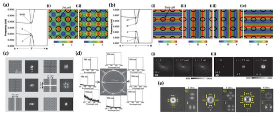
[29][44]. A common band diagram of a square-lattice photonic crystal with a circular unit cell is shown in
Figure 36a. The formation of standing waves at the band edges in such a photonic band structure can be observed. While changing the geometry of unit cells from circulars to ellipses, significant modification of the corresponding electromagnetic field distribution can be acquired, paving a novel strategy for the exact control of polarization modes, as shown in
Figure 36b. With the recent progress of metaphotonics, such a structural modification for PCSEL holds great promise not only for the novel photonic devices manipulating corresponding light emission but also for ultracompact optical devices in simplicity
[36][51].
Figure 36. (
a) Band structure of a 2D photonic crystal structure with square lattice and circular unit cell
[29][44].
Insets: (
i,ii) The corresponding electromagnetic field distributions at band edges I and II, respectively. Red and blue areas indicate the amplitudes of corresponding magnetic fields in the direction perpendicular to the plane. Arrows and thick black circles indicate the in-plane electric field vectors and the locations of lattice points, respectively. (
b) Band structure of a 2D photonic crystal structure with square lattice and elliptical unit cell
[36][51].
Insets: (
i–
iv) The corresponding electromagnetic field distributions at band edges I to IV. Unified electromagnetic field distributions can be observed at individual band edges. Thus, a linear polarization can be expected. (
c) Miscellaneous beam patterns generated by photonic-crystal lasers with engineered lattice points and/or lattice phases
[37][52]. (
d) Near-field image and the corresponding spectra distributions of a photonic crystal ring-cavity laser under the pulsed condition at room temperature
[38][53].
Insets: (
i,ii) Corresponding focusing properties of a radially polarized halo-shaped beam and a radially polarized doughnut-shaped beam, respectively. (
e) Versatile doughnut-shaped beam patterns from fabricated devices with photonic crystal structures
[39][54]. Vector beams can be observed with different lobes by the polarizer. Yellow arrows indicate the electric field direction.
In 2006, E. Miyai et al. demonstrated a series of PCSELs with miscellaneous engineered lattice points and/or lattice phases, as shown in
Figure 36c
[37][52]. As a result, originating from the asymmetry of lattice points, the symmetrical electric field will be broken while the shape of lattice points is changed to a triangular shape. Consequently, the corresponding surface-emitted beams can exhibit versatile lobe forms, namely diverse beam patterns on-demand, maintaining stable single-mode oscillation.
On the other hand, the geometrical arrangement of a photonic crystal can be another strategy. In 2012, K. Kitamura et al. presented a needle-like focus from a photonic-crystal ring-cavity laser, as shown in
Figure 36d
[38][53]. By properly manipulating the inner and outer radii of ring photonic crystal, the proposed ring-cavity laser can emit halo laser light beams with radial polarization. In addition, such a laser light emission exhibits a needle-like focus, and the corresponding spot size can shrink down to 0.4 times its wavelength with an evaluated depth of focus (DoF) longer than 10 times its wavelength for an objective lens of 0.9 numerical aperture (NA). In 2011, S. Iwahashi et al. successfully generated doughnut-shaped vector laser light beams, manifesting versatile higher-order polarization states from PCSELs with designed lattice structures, as shown in
Figure 36e
[39][54]. Moreover, a systematic analysis of the generated vector beams is conducted through the polarizer, paving a deeper understanding of the cavity symmetry of PCSELs and the consequent effects.
With the advancements for autonomous vehicles, i.e., self-driving cars, relevant methods regarding depth perception and LiDAR application are prosperously developed. The expeditious needs for miniature devices with multi functionalities are in urgent demand. For laser light scanning in LiDAR application, the aforesaid strategy with an engineered geometry of unit cell structure can be a practical solution for the monolithic integration to achieve an on-chip modification of electromagnetic field distribution. Consequently, a reliable technique for beam steering is developed, assembling an array of PCSELs
[40][55]. Each PCSEL in this array can be electronically driven, thus rapidly emitting laser light beams in distinct directions.
In 2010, Y. Kurosaka et al. demonstrated PCSELs with on-chip controllability of the beam direction, as shown in
Figure 47a
[40][55]. Based on the pioneer efforts, the corresponding output laser light beam from PCSELs can be determined by the resonant condition, and thus a properly engineered geometry of the unit cell structure in a photonic crystal is crucial
[29][36][37][38][39][41][42][44,51,52,53,54,56,57]. Therefore, they proposed relevant artificial lasing band edges with a photonic-crystal structure composed of both square and rectangular lattices. By manipulating relative lattice constants, the corresponding laser light emission in such a PCSEL device with composite photonic-crystal structures can achieve on-chip controllability in a range of directions. It is worth mentioning that beam steering via resonance detuning is proposed by M. T. Johnson et al. in 2013
[43][58]. Surface etched photonic crystals on VCSEL array elements are employed for investigating the dynamic coupled-mode theory. Thus, a complete theoretical connection between injected currents and the beam steering direction is established. Accordingly, several surface etched photonic crystals on laser devices are demonstrated by K. D. Choquette’s group, paving interesting insights into miscellaneous responses and relevant manipulation of laser devices with photonic-crystal structures
[43][44][45][46][47][48][49][50][58,59,60,61,62,63,64,65].
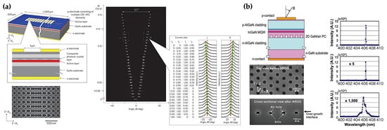
Figure 47. (
a) Schematic illustration of device structure and the corresponding on-chip beam-steering functionality
[40][55]. The bottom left side of scanning electron microscope (SEM) image shows a portion of fabricated composite photonic crystal with the square and rectangular lattice structures. (
b) Schematic illustration of the GaN-based photonic-crystal laser device and the corresponding emission spectra above the current threshold
[51][66]. The bottom left side of SEM images show the top view and the cross-sectional view before and after the fabrication of air holes retained overgrowth, respectively. As a result, the well-defined GaN/air periodic structure inside the GaN epitaxial layer can be observed.
On the one hand, extending the lasing wavelength range provides a capacious application field
[51][52][53][66,67,68]. In 2008, H. Matsubara et al. proposed a GaN-based PCSEL, emitting laser light beams in the blue-violet regime, as shown in
Figure 47b
[51][66]. To construct a two-dimensional GaN/air photonic-crystal structure, a new fabrication called air holes retained overgrowth is developed, exploiting the particular characteristics of GaN growth. Meanwhile, this new fabrication can prevent the use of the aforesaid wafer fusion technique and the complicated etching techniques in a GaN system
[18][54][55][33,69,70]. Consequently, a current-driven PCSEL with a laser light emission at 406.5 nm was successfully created. Moreover, considering a high-power PCSEL operation with narrow beam divergence, the mastery of band-edge resonance along with engineering the geometry of the unit cell structure is crucial
[56][57][58][59][60][61][71,72,73,74,75,76]. Relevant effects during the growth of photonic-crystal air holes are profoundly investigated by T. C. Lu’s group
[56][61][71,76].
4. High-Power Operation with the Concept of Double-Lattice Structure
The mastery of band-edge resonance along with engineering the geometry of unit cell structure for a PCSEL provides not only the corresponding light-emitting controllability but also a crucial part in the high-power operation with narrow beam divergence. To achieve a high-power operation, an air-hole-retained regrowth method is thereby developed, preventing the interface of discontinuous crystallinity while using the aforesaid wafer fusion technique
[18][62][33,77]. Regarding engineering the geometry of unit cell structure, an asymmetric lattice-point shape is hence exploited, namely a square-lattice photonic crystal with right-angled triangular lattice points. Moreover, a regrowth method for epitaxy to bury the etched structure is also investigated to improve the stability of lasing oscillation, generating a lower refractive index contrast at the interface
[63][78]. It is worth mentioning that a 0.2 W class PCSEL device that revolved around these engineered photonic crystals has been commercially available since 2013
[64][79].
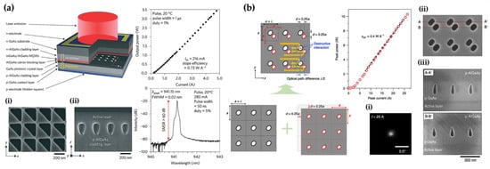
In 2014, K. Hirose et al. demonstrated a watt-class PCSEL, as shown in
Figure 58a
[65][80]. For such a PCSEL structure, the cladding layer, MQW layers, and blocking layer are grown in sequence. Next, a
p-GaAs layer is grown for preparing photonic crystals on an
n-GaAs substrate. The corresponding lattice constant of fabricated square-lattice photonic crystal with right-angled triangular lattice points is exactly aligned with the band-edge mode at Γ-point, emitting light from MQW layers at an accurate wavelength. Finally, the
p-type cladding layer and contact layer are directly grown on the as-prepared photonic crystal patterns via the air-hole-retained regrowth method based on metal–organic vapor phase epitaxy (MOVPE). Such a regrowth method exploits the innate difference in growth rates depending on distinct crystalline facets. As a result, the burial air holes can be retained near the active layer. Moreover, to obtain a high-power operation, a sufficient extraction for output light emission is necessary. Thus, the asymmetric lattice-point shapes, namely the right-angled triangular lattice points, herein are also employed to break the symmetrical electric field, increasing the surface-emitted beams. Consequently, with these efforts, such a PCSEL exhibits a watt-class laser light emission, up to 1.5 W output power. While operating with an output power of 0.5 W, the overall divergence angle is less than 0.5°, suggesting a marvelous beam quality.
Figure 58. (
a) Schematic illustration of device structure and the corresponding lasing characteristics operated under room temperature pulsed conditions
[62][77]. A watt-class laser light emission with high beam quality can be achieved with such a photonic-crystal laser device.
Insets: (
i,ii) The SEM images show the top view and the cross-sectional view before and after the burial by metal–organic chemical vapor deposition (MOCVD) regrowth, respectively. After burial, well-defined photonic-crystal air holes can be observed. (
b) Schematic illustration for the concept of a double-lattice photonic crystal and the corresponding lasing characteristic operated under room-temperature pulsed conditions
[30][45]. With the adoption of such double-lattice photonic-crystal structure, remarkable 10-watt-class laser light emission with quite narrow beam divergence can be attained.
Insets: (
i) Measured far-field pattern for such a laser device operated with an injection current of 25 A. A quite narrow divergence angle of less than 0.3° can be observed. (
ii,iii) The SEM images show the top view and the cross-sectional view before and after the MOVPE regrowth technique, respectively.
To further attain a high-power operation, namely toward a 10-watt-class laser light emission, the lasing area in a photonic crystal should be expanded, obtaining enough gain for light amplification. Holding a selective lasing oscillation in fundamental mode is vital for a high-power laser light emission. However, with the existence of sufficient field intensity around the photonic-crystal edge, a multimodal lasing oscillation usually occurs while enlarging the photonic-crystal area. Moreover, due to the shrinkage of threshold gain margin with an enlarged lasing area, namely an implicit threshold difference among the fundamental mode and higher-order modes, the multimodal lasing oscillation thereby is inevitable in an expanded conventional photonic crystal. Subsequently, the concept of the double-lattice structure emerges to roll with the punches
[30][65][66][45,80,81].
Thus, in 2019, M. Yoshida et al. proposed a modified photonic crystal with the concept of double-lattice structure to overcome this challenge, as shown in
Figure 58b
[30][45]. For such a modified photonic crystal, the double-lattice structure can provide a proper optical path difference between the backward diffracted light beams with a phase difference of 180°, thus destructively interfering with these in-plane light beams. Therefore, relevant optical modes spread out, and the lasing area can be expanded. Moreover, this expanded lasing area can maintain a widened threshold gain margin as well, leading to the suppressed higher-order modes. In the proposed modified photonic crystal, the corresponding resonator area is even increased up to 500 μmΦ. A remarkable 10-watt-class laser light emission with quite a narrow beam divergence can be attained. The asymmetry of lattice points can be adopted as well, paving a further optimization. In addition to the double-lattice structure, the use of topology can be another novel way to manipulate relevant properties inside the cavity
[67][68][69][82,83,84].
Furthermore, in 2021, M. Yoshida et al. considered a PCSEL with the backside reflection of distributed Bragg reflector (DBR) mirror, increasing the corresponding extraction and efficiency for output light emission
[70][85]. As a result, a 10-watt-class laser light emission can be acquired with an extraordinary beam divergence of 0.17° (the 1/e
2 beam width) and 0.1° (the full width at half maximum, FWHM). In other words, nearly diffraction-limited beam divergence is achieved in such a 500 μmΦ resonator area.
5. Toward a Lens-Free and Adjustment-Free ToF LiDAR System
As the tendency of miniaturization in relevant optical technologies, ultracompact optical devices with miscellaneous functionalities are urgently needed. With the state-of-the-art progress in PCSELs, such laser devices can provide higher-power and extraordinarily narrow-divergence laser light beams while keeping a symmetric beam profile. Therefore, based on these laser devices, prospects to ameliorate the bulky form factor of common optical devices are in demand.As the tendency of miniaturization in relevant optical technologies, ultracompact optical devices with miscellaneous functionalities are urgently needed. With the state-of-the-art progress in PCSELs, such laser devices can provide higher-power and extraordinarily narrow-divergence laser light beams while keeping a symmetric beam profile. Therefore, based on these laser devices, prospects to ameliorate the bulky form factor of common optical devices are in demand.
Owing to the blossom of advancements for autonomous vehicles, i.e., self-driving cars, depth perception, and LiDAR applications are flourishing. In addition, for a ToF LiDAR system, PCSELs can be appropriate laser light sources as well. In 2021, M. Yoshida et al. proposed a 10-watt-class PCSEL with DBR, operating in pulsed mode with the repetition rate and corresponding pulse width of 1 kHz and 100 ns, respectively [85]. Moreover, in 2021, R. Morita et al. introduced the design of two-dimensionally arranged gain and loss sections, and the corresponding operation in pulsed mode can even reach astonishing results [86]. In such a well-designed PCSEL, a relevant peak power of 20 W can be achieved with the repetition rate and corresponding pulse width of 1 GHz and 35 ps, respectively.
Owing to the blossom of advancements for autonomous vehicles, i.e., self-driving cars, depth perception, and LiDAR applications are flourishing. In addition, for a ToF LiDAR system, PCSELs can be appropriate laser light sources as well. In 2021, M. Yoshida et al. proposed a 10-watt-class PCSEL with DBR, operating in pulsed mode with the repetition rate and corresponding pulse width of 1 kHz and 100 ns, respectively [70]. Moreover, in 2021, R. Morita et al. introduced the design of two-dimensionally arranged gain and loss sections, and the corresponding operation in pulsed mode can even reach astonishing results [71]. In such a well-designed PCSEL, a relevant peak power of 20 W can be achieved with the repetition rate and corresponding pulse width of 1 GHz and 35 ps, respectively.Additionally, the performance trade-offs of PCSEL technology emerge with several challenges in power scaling, modal competition, charge injection control, etc. Auspiciously, with abundant efforts, these challenges can be ameliorated and conquered [15]. For real-world applications, the thermal characteristics and relevant management of laser devices are crucial and should be concerned as well [87–92]. In 2020, M. De Zoysa et al. conducted the relevant thermal analysis for PCSELs under continuous wave (CW) operation with heat dissipation [92]. The corresponding temperature properties for an assembled double-lattice PCSEL in a water-cooling package with a highly thermally conductive sub-mount are investigated, providing a practical paradigm for high-power operation. Nowadays, artificial intelligence-assisted technology can be even adopted for the fabrication as well [93]. Thus, as shown in Figure 9, these demonstrated paradigms can promise pavements toward a lens-free and adjustment-free ultracompact ToF LiDAR system soon.
Additionally, the performance trade-offs of PCSEL technology emerge with several challenges in power scaling, modal competition, charge injection control, etc. Auspiciously, with abundant efforts, these challenges can be ameliorated and conquered [2]. For real-world applications, the thermal characteristics and relevant management of laser devices are crucial and should be concerned as well [72][73][74][75][76][77]. In 2020, M. De Zoysa et al. conducted the relevant thermal analysis for PCSELs under continuous wave (CW) operation with heat dissipation [77]. The corresponding temperature properties for an assembled double-lattice PCSEL in a water-cooling package with a highly thermally conductive sub-mount are investigated, providing a practical paradigm for high-power operation. Nowadays, artificial intelligence-assisted technology can be even adopted for the fabrication as well [78]. Thus, as shown in Figure 6, these demonstrated paradigms can promise pavements toward a lens-free and adjustment-free ultracompact ToF LiDAR system soon.
Figure 69. Development progress of PCSEL technology toward an ultracompact ToF LiDAR system [8][9][18][19][30][37][39][40][51][62][71].
Development progress of PCSEL technology toward an ultracompact ToF LiDAR system [21,22,33,34,45,52,54,55,66,77,86].