Your browser does not fully support modern features. Please upgrade for a smoother experience.
Please note this is a comparison between Version 2 by Conner Chen and Version 1 by Junjie Li.
Rigid templates are defined as opposed to soft templates, and are made of hard materials. Rigid templates have good chemical stability and mechanical rigidity, which are mostly used for the fabrication of nanostructure arrays. A wide choice of rigid templates is available, such as silicon, anodic aluminum oxide, carbon, silica spheres, biological structures, and so forth.
- atomic layer deposition
- sacrificial templates
- 3D nanostructures
1. Si Templates
1. Si Templates
Generally, the ALA method based on sacrificial templates to obtain the 3D nanostructures includes three steps. Firstly, the sacrificial patterned templates can be fabricated using various advanced nano-techniques. The critical techniques for fabricating Si and AAO rigid templates commonly are lithography combined with etching (dry or wet) and anodization. For soft templates electron or photoresist polymers, electron beam lithography (EBL), direct laser writing (DLW), proximity field nanopatterning (PnP), and multibeam interference lithography (MBIL) are usually utilized. As for assembled polymer templates, block copolymer (BCP), electrospinning (ES), and self-assembly (SA) are regularly employed. Then the films with a certain thickness are deposited on sacrificial templates by ALD for 3D assembly to construct 3D nanostructures. Finally, the residual templates are selectively removed by etching or a heat treatment, and 3D nanostructures shaped by the sacrificial templates can be obtained. Through this ALA method based on sacrificial templates, many kinds of 3D nanostructures could be fabricated, like nanotubes, nanopillars, nanofibers, nanonetworks, inverse opals, and even replication of biological structures [1][2][3][4]. These 3D nanostructures possess full and precise control of size and shapes, considerable reproducibility, and flexible design, making them attractive for a broad range of practical applications.
Perhaps the most well-known material to fabricate nanostructures, silicon may be the most widely investigated due to its mature fabrication process. Therefore, it is natural for researchers to fabricate 3D nanostructure replicas by utilizing silicon nanostructures as sacrificial templates. Figure 31a exhibits the fabrication routine of 3D nanostructures by ALA method through Si templates. Firstly, the Si templates are commonly prepared by lithography and etching process, resulting in templates with nanopillars or nanopores. Then the ALD process is applied sequentially and generally followed by a removal of the ALD cap on top of the structure. The last step is silicon template removal, which is done by dry or wet etching, leaving the high aspect ratio 3D nanostructures without distortion. In such a way, 3D nanostructures could be obtained, whose shape, size, and thickness can be modulated with higher resolution and high aspect ratio [32,33,34][5][6][7]. The success of this procedure is heavily dependent on the ability to etch silicon selectively and realize the perfect replication from photoresist patterns to Si templates, without destroying the ALD coatings, which also limits the diversity and resolution in nanostructure for the Si templates.
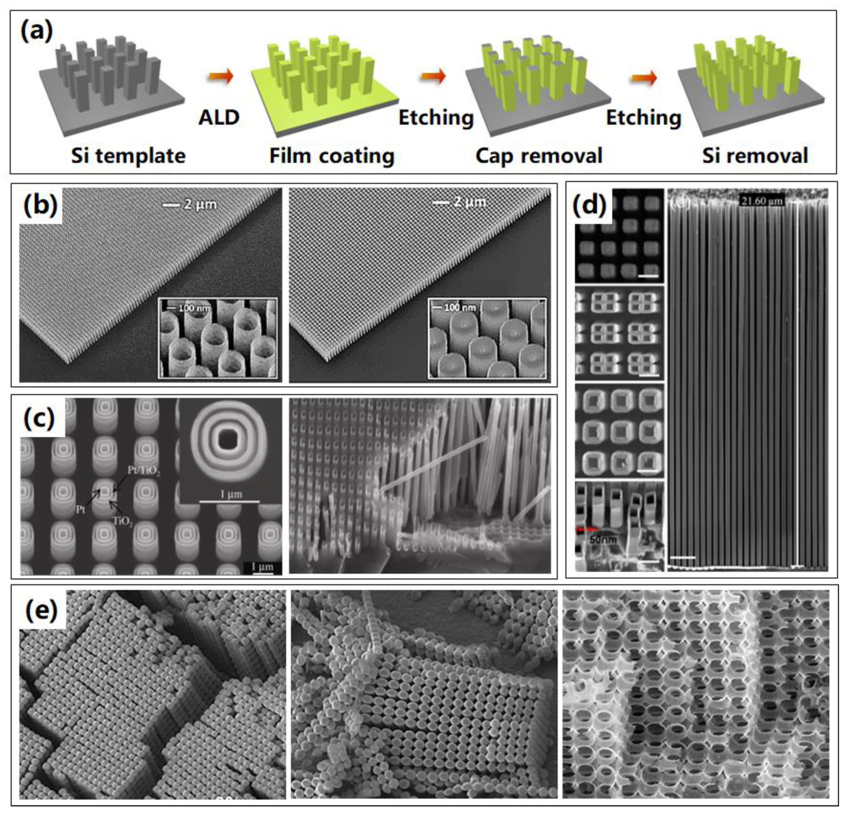
Figure 31. Representative 3D nanostructures fabricated by ALA method through Si templates. (a) Process routine of 3D nanostructures based on Si templates by ALA method. (b) Titled scanning electron microscope (SEM) images of the 3D metamaterial structures: Al-doped ZnO (AZO) nanotubes and nanopillars. The insets show an enlarged view of the metamaterials. Reprinted from [32], copyright 2017, with permission from Optical Society of America. (c) Multi-walled nested nanotube structures with alternating open annular layers after removal via chemical etching of two ALD Al2O3 sacrificial spacer layers, cleaved Si template highlighting that ALD Pt has infiltrated up to 90 µm deep into the bottom of the porous Si template. Reprinted with permission from Ref. [35]. Copyright 2011 Springer. (d) Top view SEM image of the Si nanostructures after Al2O3 film deposition by ALD, and SEM images of the top, cross-section, and tilted views of the generated Al2O3 nanotube arrays resulting from the sidewall transfer MacEtch process. Reprinted with permission from Ref. [36]. Copyright 2020 MDPI. (e) An array of hollow TiO2 micro-pearl chains viewed from the bottom and the side, and enlarged SEM images of TiO2 porous network structures. Reprinted with permission from Ref. [37]. Copyright 2008 Springer.
As shown in Figure 31b, large-area 3D Al-doped ZnO (AZO) nanopillars and nanotubes using a combination of advanced reactive ion etching and ALD techniques were fabricated through sacrificial Si templates [32][5]. It was found that the last step of Si template removal process was heavily dependent on the selective chemistry of the SF6 plasma. It was shown that silicon between AZO structures can be selectively removed with no observable influence on the ALD deposited coatings. Furthermore, complex multi-walled nested TiO2–Pt nanotubes in series have been successfully fabricated using microporous Si templates, as shown in Figure 31c (left) [35][8]. Multilayered nested nanotubes separated by sacrificial spacer layers of TiO2 (50 nm)/Al2O3 (120 nm)/Pt (25 nm)/TiO2 (25 nm)/Al2O3 (120 nm)/Pt (50 nm) were firstly fabricated, followed by removal of the Al2O3 sacrificial spacer layers and the porous Si template by using NaOH solution, resulting in the novel multi-walled nested structures. These innovative nested nanostructures have the potential to produce novel multifunctional vertically-ordered 3D nanodevices in photovoltaic and sensing technologies. Especially, optimizing the ALD process by using an additional 10 s exposure time, as-formed Pt could infiltrate up to 90 µm deep into the bottom of the porous Si template, achieving extreme high aspect ratio Pt nanotubes in Figure 31c (right).
Furthermore, ultra-high aspect ratio Al2O3 nanotube arrays with line widths as small as 50 nm, heights of up to 21 µm, and an aspect ratio of up to 420:1 were successfully fabricated, utilizing reliable sidewall transfer low-temperature Au metal assisted chemical etching (MacEtch) process, as displayed in Figure 31d [36][9]. This technique combined the advantages of the high aspect ratio nanostructure capabilities of the MacEtch with the sidewall transfer process. Such a sidewall transfer MacEtch approach was compatible with well-established silicon planar processes, and has the benefits of possessing a fully controllable linewidth and height, high reproducibility, and flexible design, making it attractive for a broad range of practical applications. Similar high aspect ratio 3D nanostructures were investigated [34][7], while Bosch process was applied to fabricate the Si template with high aspect ratio nanoholes. As long as complex Si templates could be manufactured, more complex nanostructures could be realized by replication of the complex Si templates. As shown in Figure 31e, 3D macroporous silicon template was firstly fabricated by wet etching method [37][10], then hollow TiO2 micropearl chains and networks were obtained by ALD after removal of Si template. For possible applications, the presented TiO2 micropearls are well suited as carriers for drug delivery, whereas the network structures can work as highly porous photocatalytic material.
The advantages of Si templates are the mature fabrication process, custom flexible design, and easy implementation for array fabrication. While the removal of Si templates, in which wet etching is mostly utilized, is usually complicated and contaminative. Furthermore, it is a challenge to preserve exactly the morphology of the as-deposited nanostructures.
2. AAO Templates
Another widely investigated rigid template is the anodic aluminum oxide (AAO) template. AAO is an appealing template to fabricate highly ordered and regular nanostructures, showing advantages including low cost, good compatibility, easy scalability, and flexible controllability, and has been exploited for fabricating various nanostructure arrays [38,39][11][12]. As shown in Figure 42a, the fabrication process of 3D nanostructures based on AAO template is practically accordant with Si template, while the AAO templates are usually prepared by anodization method, resulting in templates with various nanopores. Once the AAO templates are prepared, the same following processes as ALD of certain materials and removal of cap and templates are conducted successively. An AAO template possesses significant advantages due to its uniform nanochannels size, tunable pore dimensions, good mechanical strength, and thermal stability. The morphological parameters of the 3D nanostructures, such as the packing density or the aspect ratio, are fully controlled by the geometrical parameters of the AAO template.
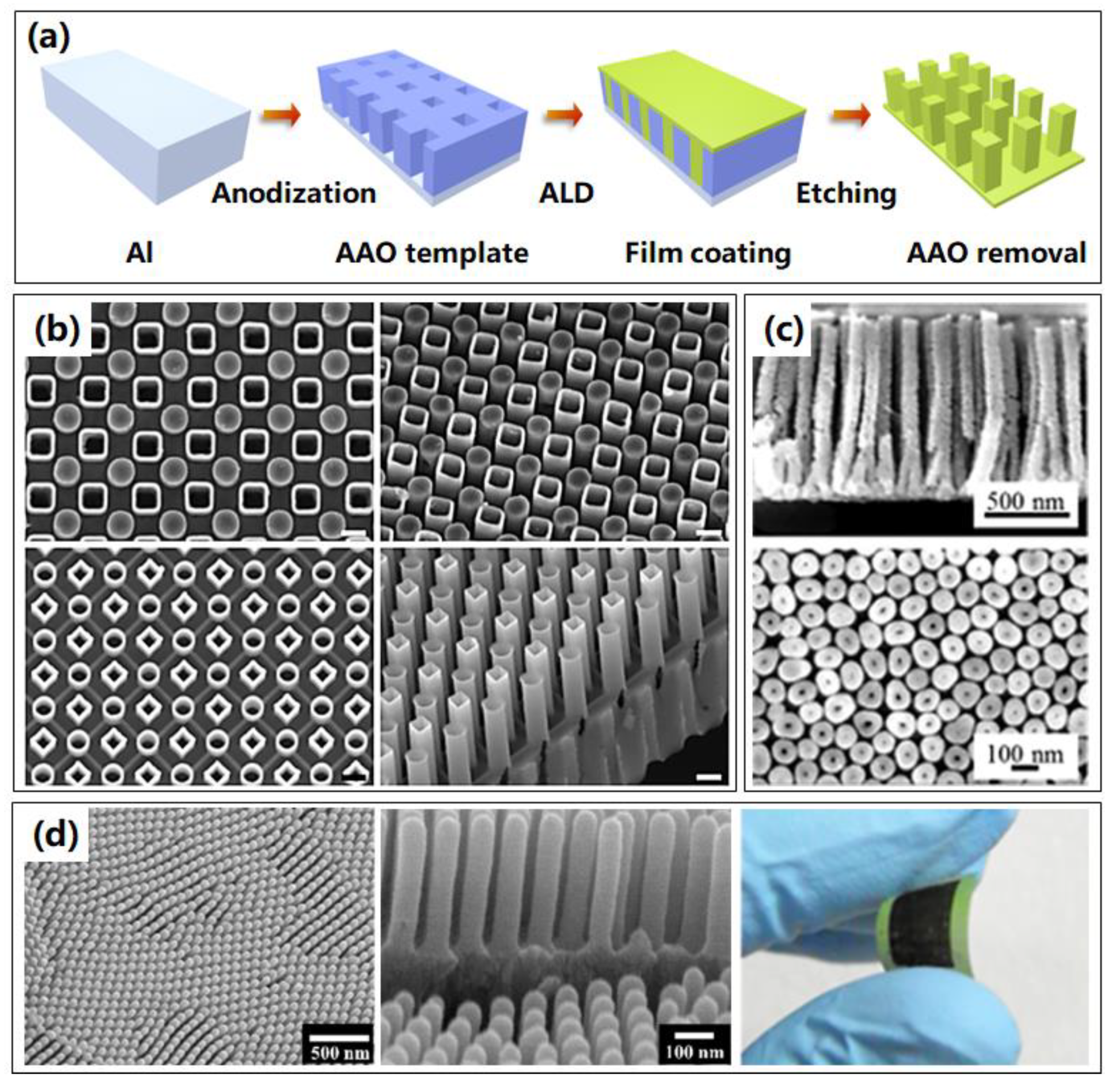
Figure 42. Typical 3D nanostructures fabricated by ALA method through AAO templates. (a) Process routine of 3D nanostructures based on AAO templates by ALA method. (b) SEM images of representative 3D binary nanostructure arrays. The upper two show nanostructures with nanopillars and nanotubes, and the lower two are nanostructures with all nanotubes. Reprinted with permission from Ref. [40], Copyright 2017 Macmillan Publishers Limited, part of Springer Nature. (c) SEM images of 3D ZnO nanowires for sensor applications. Reprinted with permission from Ref. [2], Copyright 2016 American Vacuum Society. (d) Overall and enlarged SEM images, and photograph of flexible 3D TiN nanotubes arrays. Reprinted with permission from Ref. [30]. Copyright 2020 MDPI.
Diverse binary or multi nanostructure arrays with high degrees of controllability for each of the sub-components, including material, dimension and morphology, as shown in Figure 42b, were fabricated based on ALA method through an AAO template [40][13]. This binary nanostructure originated with a distinctive binary-pore AAO template that included two dissimilar sets of pores in one matrix, where the openings of the two sets of pores were towards opposite sides of the template. They also presented proof-of-principle photoelectrodes, transistors, and plasmonic devices made with binary nanostructure arrays using different combinations of materials and morphologies, and demonstrated superior performances compared to their single-component counterparts.
Due to the high surface area, which will enlarge the contact area between structures and reactant, another important application of 3D nanostructures is sensors. A new low-temperature nanowire fabrication process using AAO sacrificial templates was presented [2][14], which allowed high aspect ratio nanowires to be readily integrated with microelectronic devices for sensor applications. As displayed in Figure 42c, the resulting ZnO nanowire array enhanced the sensor surface area by ~38 times over a conventional flat film, which was supposed to improve capacities of sensors, like sensitivity and response speed.
Flexible devices have achieved remarkable progress over the past years and have become increasingly important to many sectors. Even the AAO template is a rigid template, however, it can also be utilized to fabricate flexible devices. In 2020, the TiN nanotube arrays on flexible substrates were achieved by ALA method through AAO template [30][3], as shown in Figure 42d. The flexibility of the fabricated nanostructures was investigated using the cyclic bending and releasing method at high curvature. No noticeable cracks or delamination were detected upon operation after 1000 cycles. Meanwhile, delamination and faceted phenomena were not observed after 3000 cycles, implying that this method has a great potential for application in flexible systems as a 3D electrode.
For AAO templates, some problems of complicated post processes are inevitable, and the removal of the AAO template using chemical solvent is a big problem to be compatible with the fabrication of conventional Si-based integrated circuits. The compatibility with other common mature industrial processes needs to be developed further and the environmental concerns should be resolved.
3. Biological Templates
Apart from the artificial templates discussed above, the rigid templates even show enormous flexibilities in biological structure. Nature provides extensive micro-nanostructures, which could be utilized as templates to fabricate various 3D structures, such as photonic crystals, fiber networks, etc. Compared with other rigid templates, the bio-templates have the advantage of availability in a wide variety of sources, complex structure, nontoxicity, and easy removal, and they have great potential to be used as templates for the synthesis of other materials. A variety of biological templates have been utilized to fabricate 3D nanostructures, such as veritable biological templates of butterfly wings, fly eyes, cotton, and tubular trichome on legume, as shown in Figure 53. The first bio-inspired novel biostructures with the scale of a butterfly wing [31][4] were replicated through an Al2O3 coating by a low-temperature ALD process. An inverted 3D biostructure was achieved by removing the butterfly wing template at high temperature, forming a polycrystalline Al2O3 shell biostructure with precisely controlled thickness, as presented in Figure 53a. Other antireflection nanostructures were fabricated by replicating fly eyes using the same process, as shown in Figure 53b, indicating potential applications in optical coating, sensing, or lens arrays [41][15]. Furthermore, Tian et al. [42][16] deposited Al2O3 on the surface of low-cost cotton fibers, and hollow Al2O3 fibers were synthesized after the elimination of sacrificial cotton templates, and retained the micro- and macrostructures of the cotton. This low-weight Al2O3 fiber network with elastic and porous 3D structures overcomes the issues resulting from the 2D rigid Al2O3 layer and provides a low overpotential and dendrite-free growth of lithium metal, as shown in Figure 53c. Furthermore, a biomorphic mixed metal oxide framework through a legume bio-templated synthesis method by using a combination of ALD-in situ growth-calcination [43][17], showing potential applications in catalysis and adsorbents, was reported and investigated, as shown in Figure 53d.
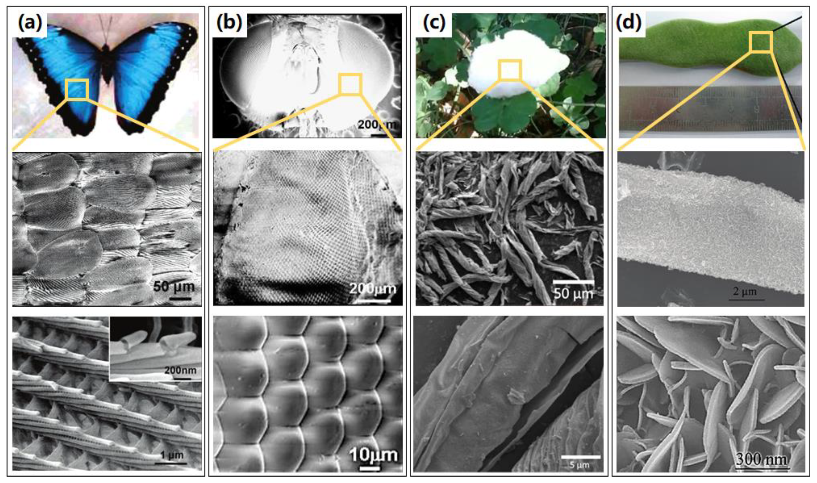
Figure 53. Attractive 3D nanostructures fabricated by ALA method through biological templates, with the photo image of veritable biological template, overall and enlarged SEM images in local area. (a) The biological templates of butterfly wings, with overall and enlarged SEM images of the alumina replicas of the butterfly wings. Reprinted with permission from Ref. [31], Copyright 2006 American Chemical Society. (b) Veritable biological templates of fly eyes and SEM images of the alumina replica of a fly compound eye. Reprinted with permission from Ref. [41], Copyright 2008 IOP Publishing Ltd. (c) Veritable biological templates of cotton, overall, and enlarged SEM images of fibrous Al2O3 nanotube network. Reprinted with permission from Ref. [42], Copyright 2018 Wiley-VCH Verlag GmbH & Co. KGaA, Weinheim. (d) Veritable biological templates of tubular trichome on legume, with SEM images of mixed metal oxides framework obtained using a combination of ALD in situ growth calcination. Reprinted with permission from Ref. [43], Copyright 2009 American Chemical Society.
Other groups also investigated various nanostructures with remained biological templates, which enriched the feasibility and functionality of biological templates [44,45,46][18][19][20]. The advantages of biological templates are low cost, natural structural diversity, and highly accessible, which show enormous possibilities in commercial applications and deserve to be investigated further. However, the low chemical stability at high temperature, low tolerance for multistep fabrication processes, and weak reusability impede the development of the biological templates.
4. Other Rigid Templates
Except the templates discussed above, there are several special rigid templates that could be utilized to fabricate 3D nanostructures, such as cellulose, carbon coil, carbon spheres, and silica spheres, as schematically shown in Figure 64. Ortal et al. [47][21] deposited TiO2 nanofilms by ALD onto cellulose microfibers, leading to the formation of chiral nanofilms with a spatial fibrous structure, which show potential applications in enantioselective areas. The obtained fibers on cellulose fibers and after cellulose extraction are displayed in Figure 64a. Natural cellulose was also investigated to prepare TiO2, ZnO, and Al2O3 nanotube aerogels, resulting in an efficient humidity sensor with a fast response [48][22].
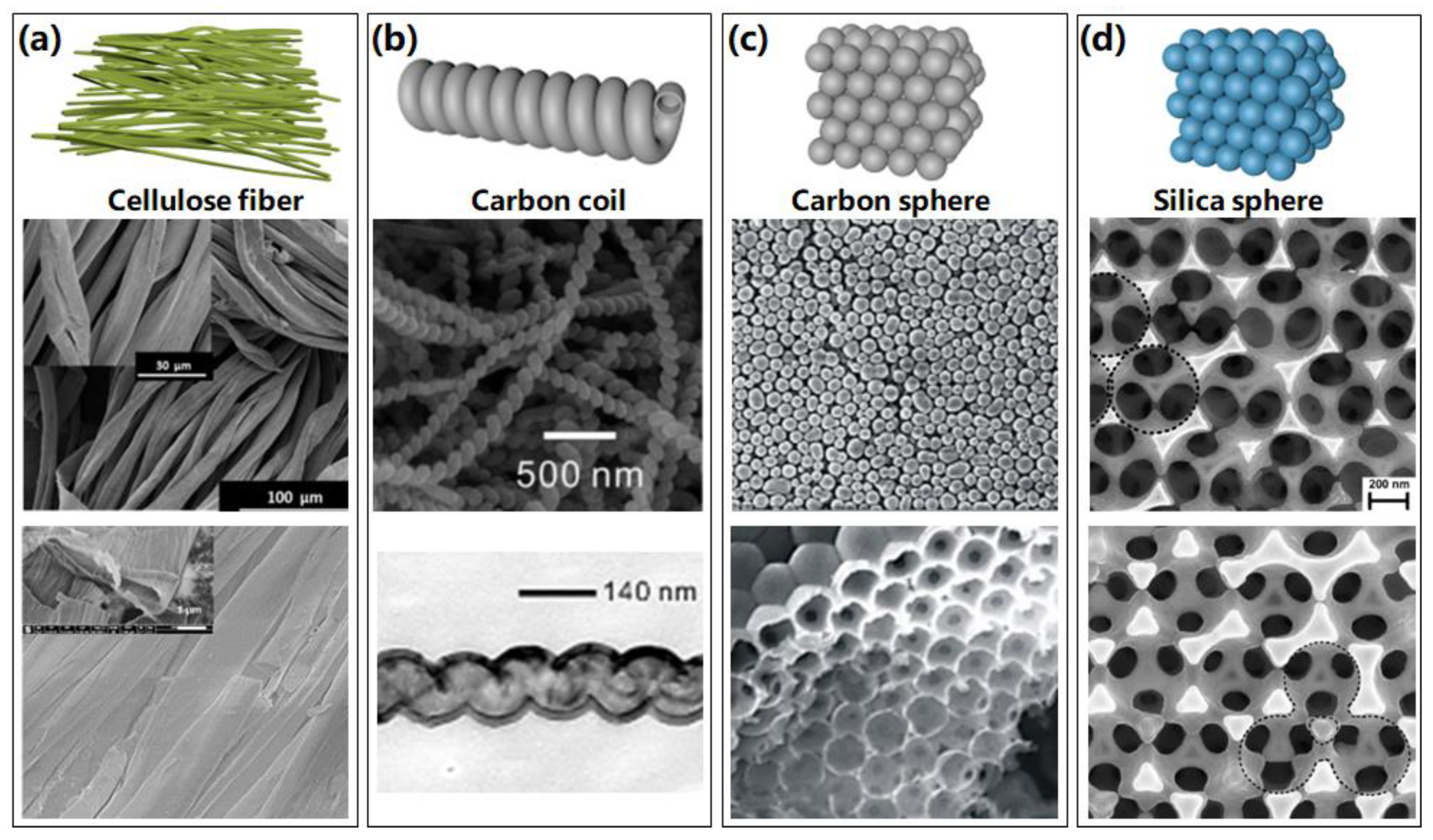
Figure 64. Several special 3D nanostructures fabricated by atomic layer assembly method through cellulose, carbon, and silica templates. (a) Schematic images of cellulose fiber templates, SEM images of TiO2 fibers on cellulose fibers, and SEM images of Al2O3 nanofibers after cellulose extraction. Reprinted with permission from Ref. [47], Copyright 2017 American Chemical Society. (b) Schematic images of carbon coil templates, SEM image of as-formed helical Al2O3 nanotube after removal of templates, and TEM image of TiO2 helical nanotubes after removal of templates. Reprinted with permission from Ref. [49], Copyright 2010Wiley-VCH Verlag GmbH & Co. KGaA, Weinheim. (c) Schematic images of carbon sphere templates, and SEM images of veritable templates of carbon sphere opal and TiO2 inverse opal. Reprinted with permission from Ref. [50], Copyright 2020 Elsevier. (d) Schematic images of silica spheres templates, and SEM images of TiO2 close-packed inverse opals and non-close-packed inverse opals. Reprinted with permission from Ref. [51], Copyright 2006 WILEY-VCH Verlag GmbH & Co. KGaA, Weinheim.
A forest of 1D anatase TiO2 nanoparticle chains was also synthesized based on ALA method using carbon nanotubes as sacrificial templates [52][23]. The resulting self-supported structure of fully crystallized nanoparticles offers a porous network with a large surface area. As shown in Figure 53c and Figure 64b, carbon nanocoils [49][24] and nanospheres [50][25] were also investigated and used as sacrificial templates to prepare distinctive helical nanotubes and inverse opal photonic crystals, respectively, indicating potential applications in sensors, mechanical springs, and photocatalysis areas. Similarly, silica nanospheres [51][26] were utilized to fabricate inverse opal photonic crystals as shown in Figure 64d, which revealed a potential application in photocatalytic and solar cells.
However, the carbon and silica templates possess the disadvantages of inflexible structure and low variability, which restrict the realization of custom structures and functional expansion based on those templates. With the development of modern techniques, it is believed that more kinds of rigid templates will be fabricated and investigated to achieve 3D nanostructures based on ALA methods.
References
- Zhou, K.; Li, P.; Zhu, Y.; Ye, X.; Chen, H.; Yang, Y.; Dan, Y.; Yuan, Y.; Hou, H. Atomic Layer Deposition of ZnO on TiO2 Nanofibers for Boosted Photocatalytic Hydrogen Production. Catal. Lett. 2020, 151, 78–85.
- Wei, Z.; Ruisheng, Y.; Guangzhou, G.; Yuancheng, F.; Xuyue, G.; Peng, L.; Quanhong, F.; Fuli, Z.; Changzhi, G.; Junjie, L. Titanium dioxide metasurface manipulating high-efficiency and broadband photonic spin Hall effect in visible regime. Nanophotonics 2020, 9, 4327–4335.
- Yun, S.; Kim, S.-J.; Youn, J.; Kim, H.; Ryu, J.; Bae, C.; No, K.; Hong, S. Flexible 3D Electrodes of Free-Standing TiN Nanotube Arrays Grown by Atomic Layer Deposition with a Ti Interlayer as an Adhesion Promoter. Nanomaterials 2020, 10, 409.
- Huang, J.; Wang, X.; Wang, Z.L. Controlled Replication of Butterfly Wings for Achieving Tunable Photonic Properties. Nano Lett. 2006, 6, 2325–2331.
- Shkondin, E.; Takayama, O.; Panah, M.E.A.; Liu, P.; Larsen, P.V.; Mar, M.D.; Jensen, F.; Lavrinenko, A.V. Large-scale high aspect ratio Al-doped ZnO nanopillars arrays as anisotropic metamaterials. Opt. Mater. Express 2017, 7, 1606–1627.
- Tian, J.-L.; Wang, G.-G.; Zhang, H.-Y.; Han, J.-C. Nanopore diameter-dependent properties of thin three-dimensional ZnO layers deposited onto nanoporous silicon substrates. Ceram. Int. 2017, 43, 5173–5181.
- Shkondin, E.; Takayama, O.; Lindhard, J.M.; Larsen, P.V.; Mar, M.D.; Jensen, F.; Lavrinenko, A.V. Fabrication of high aspect ratio TiO2 and Al2O3 nanogratings by atomic layer deposition. J. Vac. Sci. Technol. A Vac. Surf. Film. 2016, 34, 031605.
- Gu, D.; Baumgart, H.; Tapily, K.; Shrestha, P.; Namkoong, G.; Ao, X.; Müller, F. Precise control of highly ordered arrays of nested semiconductor/metal nanotubes. Nano Res. 2010, 4, 164–170.
- Li, H.; Xie, C. Fabrication of Ultra-High Aspect Ratio (>420:1) Al2O3 Nanotube Arraysby Sidewall TransferMetal Assistant Chemical Etching. Micromachines 2020, 11, 378.
- Langner, A.; Knez, M.; Müller, F.; Gösele, U. TiO2 microstructures by inversion of macroporous silicon using atomic layer deposition. Appl. Phys. A 2008, 93, 399–403.
- Wen, L.; Wang, Z.; Mi, Y.; Xu, R.; Yu, S.-H.; Lei, Y. Designing Heterogeneous 1D Nanostructure Arrays Based on AAO Templates for Energy Applications. Small 2015, 11, 3408–3428.
- Zhou, Z.; Nonnenmann, S.S. Progress in Nanoporous Templates: Beyond Anodic Aluminum Oxide and Towards Functional Complex Materials. Materials 2019, 12, 2535.
- Wen, L.; Xu, R.; Mi, Y.; Lei, Y. Multiple nanostructures based on anodized aluminium oxide templates. Nat. Nanotechnol. 2017, 12, 244–250.
- Clavijo, W.P.; Atkinson, G.M.; Castano, C.E.; Pestov, D. Novel low-temperature fabrication process for integrated high-aspect ratio zinc oxide nanowire sensors. J. Vac. Sci. Technol. B Nanotechnol. Microelectron. Mater. Process. Meas. Phenom. 2016, 34, 022203.
- Huang, J.; Wang, X.; Wang, Z.L. Bio-inspired fabrication of antireflection nanostructures by replicating fly eyes. Nanotechnology 2007, 19, 025602.
- Tian, R.; Feng, X.; Duan, H.; Zhang, P.; Li, H.; Liu, H.; Gao, L. Low-Weight 3D Al2 O3 Network as an Artificial Layer to Stabilize Lithium Deposition. ChemSusChem 2018, 11, 3243–3252.
- Zhao, Y.; Wei, M.; Lu, J.; Wang, Z.L.; Duan, X. Biotemplated Hierarchical Nanostructure of Layered Double Hydroxides with Improved Photocatalysis Performance. ACS Nano 2009, 3, 4009–4016.
- Ding, Y.; Xu, S.; Zhang, Y.; Wang, A.C.; Wang, M.H.; Xiu, Y.; Wong, C.P.; Wang, Z.L. Modifying the anti-wetting property of butterfly wings and water strider legs by atomic layer deposition coating: Surface materials versus geometry. Nanotechnology 2008, 19, 355708.
- Rodríguez, R.E.; Agarwal, S.P.; An, S.; Kazyak, E.; Das, D.; Shang, W.; Skye, R.; Deng, T.; Dasgupta, N.P. Biotemplated Morpho Butterfly Wings for Tunable Structurally Colored Photocatalysts. ACS Appl. Mater. Interfaces 2018, 10, 4614–4621.
- Liu, F.; Liu, Y.; Huang, L.; Hu, X.; Dong, B.; Shi, W.; Xie, Y.; Ye, X. Replication of homologous optical and hydrophobic features by templating wings of butterflies Morpho menelaus. Opt. Commun. 2011, 284, 2376–2381.
- Lidor-Shalev, O.; Pliatsikas, N.; Carmiel, Y.; Patsalas, P.; Mastai, Y. Chiral Metal-Oxide Nanofilms by Cellulose Template Using Atomic Layer Deposition Process. ACS Nano 2017, 11, 4753–4759.
- Korhonen, J.T.; Hiekkataipale, P.; Malm, J.; Karppinen, M.; Ikkala, O.; Ras, R.H.A. Inorganic Hollow Nanotube Aerogels by Atomic Layer Deposition onto Native Nanocellulose Templates. ACS Nano 2011, 5, 1967–1974.
- Deng, S.; Verbruggen, S.W.; He, Z.; Cott, D.J.; Vereecken, P.M.; Martens, J.A.; Bals, S.; Lenaerts, S.; Detavernier, C. Atomic layer deposition-based synthesis of photoactive TiO2 nanoparticle chains by using carbon nanotubes as sacrificial templates. RSC Adv. 2014, 4, 11648–11653.
- Qin, Y.; Kim, Y.; Zhang, L.; Lee, S.-M.; Bin Yang, R.; Pan, A.; Mathwig, K.; Alexe, M.; Gösele, U.; Knez, M. Preparation and Elastic Properties of Helical Nanotubes Obtained by Atomic Layer Deposition with Carbon Nanocoils as Templates. Small 2010, 6, 910–914.
- Bakos, L.P.; Karajz, D.; Katona, A.; Hernadi, K.; Parditka, B.; Erdélyi, Z.; Lukács, I.; Hórvölgyi, Z.; Szitási, G.; Szilágyi, I.M. Carbon nanosphere templates for the preparation of inverse opal titania photonic crystals by atomic layer deposition. Appl. Surf. Sci. 2020, 504, 144443.
- Graugnard, E.; King, J.S.; Gaillot, D.P.; Summers, C.J. Sacrificial-Layer Atomic Layer Deposition for Fabrication of Non-Close-Packed Inverse-Opal Photonic Crystals. Adv. Funct. Mater. 2006, 16, 1187–1196.
More