Your browser does not fully support modern features. Please upgrade for a smoother experience.
Please note this is a comparison between Version 1 by Qiancheng Zhao and Version 3 by Vivi Li.
The advent of metasurface technology has revolutionized the field of optics and photonics in recent years due to its capability of engineering optical wavefronts with well-patterned nanostructures at the subwavelength scale. Meanwhile, inspired and benefited from the tremendous success of the “lab-on-fiber” concept, the integration of metasurface with optical fibers, due to its powerful function of light manipulation and shaping in the 2D version, has drawn particular interest in the last decade, which truly establishes a novel technological platform for the development of “all-in-fiber" metasurface-based devices.
- metasurface technology
- nanostructures
- lab-on-fiber
- optical fiber metasurfaces
1. Introduction
Optical fiber has long been a well-established medium since the first demonstration of silica-based fiber with low-loss transmission less than 20 dB/km in the 1970s [1]. Benefiting from its extraordinary features such as perfect light guiding, light volume, chemical inertness, and immunity to electromagnetic interference, a myriad of optical fiber-based applications have been realized, which has greatly revolutionized the optical sensing [2][3][4][5][6][2,3,4,5,6] and telecommunication industry [7][8][9][7,8,9] in the last five decades. Despite the tremendous success of optical fiber technology, it turns out that there remain several challenges that obstruct the further progress of optical fiber-based devices. The optical properties such as the propagation direction of guided modes, amplitude, mode profile, polarization states, are hardly to be altered after the fiber drawing fabrication process. Moreover, the divergence of output transmitted light and chromatic dispersion of the optical fiber also limits the practical applications in long-haul transmission systems. In this regard, the recent concept of “lab-on-fiber” has opened up a new pathway to functionalize conventional fibers for multiple applications (e.g., environmental sensing, biomedicine, clinical diagnosis [10][11][12][10,11,12]), with the enhanced light-matter interactions introduced by the dielectric or metallic nanostructured patterns embedded on the facet of optical fibers. Undoubtedly, the lab-on-fiber paradigm has greatly boosted the creation of novel plug-and-play “all-in-fiber” devices that are accessible in various application scenarios. However, most of the conventional nanostructures are formed by artificial 3D metamaterials (e.g., “meta-atoms”). The fabrication process of 3D metamaterials is labor-intensive and costly, which brings complexity and impediments for practical optical applications.
Fortunately, the appearance of metasurface technology in the last decade has further brought disruptive innovations to the nanophotonic field. The metasurfaces, based on the phase discontinuities with 2D counterparts of metamaterials, could flexibly engineer the properties (e.g., phase, amplitude, and polarization) of the incident light. Therefore, a number of applications have been surged, including beam steering [13], aberration-free focusing metalenses [14], polarization control [15][16][15,16], holography [17][18][19][17,18,19], and imaging [20][21][22][20,21,22]. Inspired by the lab-on-fiber technology, the integration of metasurfaces on optical fibers, as a novel landmark in the lab-on-fiber realm, has attracted enormous attention in recent years. The flexibility, biocompatibility, and mechanical robustness have made optical fibers excellent platforms to be linked to metasurface technology, which is expected to leverage the functionalities pertaining to optical fiber technologies to be applied to real-world scenarios.
2. Basic Concepts and Principle of Metasurfaces
Metasurfaces are typically made up of arrays of antennas that are spatially at subwavelength scale with varying geometric parameters. The light propagating through metasurfaces will undergo varying spatially optical responses and thus be shaped by the phase discontinuities (defined as the abrupt phase change over a distance compared to wavelength). The working principle of metasurfaces was systematically demonstrated by Yu and Capasso in 2011, where the generalized Snell’s laws were formulated with the introduction of the concept of phase discontinuities [13]. Briefly, the working principle of metasurface can be explained from the perspective of Huygen’s principle: Each point on the interface can be regarded as an independent source and generated as a sphere wavelet, and a new wavefront is thus created by the interference of these wavelets. For a regular nonstructured surface, there is no change of propagation direction for the incident light. However, in the case of inhomogeneous metasurface consisting of arrays of resonators (e.g., antenna, nanopillars, nanobricks, etc.), the wavefront will be reconstructed due to the distinct phase response of these spatially arranged resonators, as indicated by Figure 1a,b. To further analyze the phenomenon of reflection and refraction of light interacting with metasurfaces, Fermat’s principle can be applied, stating that two infinitesimally close paths should have optical phase difference of zero (so-called “stationary phase”). These optical paths include the inherent propagation phase and the phase change induced at the interface, as shown in Figure 1c.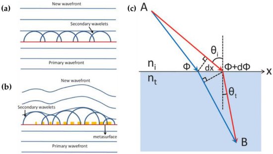
Figure 1. Schematics showing the Huygens’s principle with optical wavefront impinging on (a) nonstructured surface, and (b) a metasurface. Reprinted with permission from Ref. [23]. Copyright 2015 IEEE Photonics Society. (c) Schematic of derived generalized Snell’s law of refraction. Reprinted with permission from Ref. [13]. Copyright 2011 American Association for the Advancement of Science.
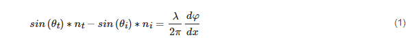 where θt and θi are the refraction and incident angles, respectively, and nt and ni are the refractive indices of the two media. The constant phase gradient, denoted as dφ/dx, is determined by the specific geometries and spatial arrangements of the resonators. Equation (1) also implies that the refracted beam can be directed arbitrarily. Furthermore, under the condition nt < ni, the critical angles under the total internal reflection condition can be satisfied and derived, as:
 Similarly, in the case of reflection with gradient metasurface, the generalized Snell law can be rewritten as:
 where θr is the reflection angle. It is seen from Equation (3) that the anomalous reflection is no longer equal to the incident angle, which differs significantly from the conventional specular reflection. In addition, Equation (3) indicates that there exists a critical angle beyond which the reflected beam becomes evanescent, which is expressed as:
 As seen from Equations (1)–(4), the light manipulation is closely associated with the phase gradient induced by the optical resonators constituting the 2D metasurfaces. The optical resonators can be selected from a wide range such as dielectric resonators, quantum dots, nano-crystals, and plasmonic antennas. However, it should be noted that the resonators have to satisfy the following requirements: (1) they should have subwavelength geometric parameters to be arranged at subwavelength scale with limited transmission loss. (2) The phase modulation of these resonators should cover the entire 2π range. (3) The scattered optical amplitude should be uniform and large across the metasurface array. Based on the principles and physics of metasurfaces, Yu and Capasso et al. have successfully pioneered a variety of flat optical components based on metasurfaces, including metalens [24], quarter-wave plates [15], vortex plates [25], and holograms for vortex beam generation [26]. In particular, successful implementation of the metasurface-based collimating lens on the facets of semiconductor lasers to control the far-field laser emissions (e.g., divergence angle [27], output power [28]) has shown promising inroads towards the production of metasurface-integrated devices. This would be of great value to propel the optical fiber-integrated metasurfaces, because in both platforms the light propagation is well confined in the optical waveguide.
3. Applications of Optical Fiber Meta-devices
Illuminated by the successful integration of metasurface with the well-established platform of semiconductor lasers for wavefront engineering, there is sufficient grounds that the metasurface technology could also bring new features to conventional optical fibers to launch a novel class of all-fiber devices and components: (1) the metasurface arrays can be readily patterned on the facets (e.g., end face of the fiber core, the side face of D-shaped fiber) of optical fibers to interact with either the confined or evanescent fields [29][30][31][29,30,31]. (2) The compact resonators of metasurface nanostructures on the optical fiber platforms can have strong interactions with either the electric field or magnetic field of the guided light, thus controlling the optical impedance with modified transmission or reflection properties. (3) The integrated metasurface with high refractive index materials is capable of modulating the optical properties of the guided mode, including the phase, amplitude, and wavevector. Therefore, optical fiber metasurface-based devices have sprung up during the last decade and have been exploited in many strategic applications, ranging from optical processing and communication to environmental sensing, biomedicine, and security. In the following, the specific application scenarios, design methods, and brief physics of optical fiber-integrated metasurface-based devices are categorized, reviewed, and discussed accordingly.3.1. Function of Light Beam Focusing
One of the most pronounced and repetitively reported functions of fiber-integrated metasurface is the light beam, focusing on fiber guided fundamental mode. Typically, to transfer the input plane wavefronts to the focused spherical ones, the phase retardation of the predesigned metalens should follow the hyperbolic phase profile, which is expressed as [32][33][32,33]:

where (x, y) refers to the spatial coordinate in which each unit cell of the metalens is located, f is the designed focal length, and λ is the operating wavelength. To realize the target hyperbolic phase distribution, several phase modulation methods for the spatially distributed nanopillars can be considered. Depending on the polarization sensitivity of the incident beam, the phase modulation methods can be classified into two types: one is the propagation phase modulation [34], in which the phase difference is mapped by square cylinders or cylinders utilizing varying side lengths or diameters. Each nanofin can be regarded as a waveguide and thus introduce the waveguiding effect as the following [35]:

where neff represents the effective index of the fundamental mode (HE11) and H is the propagation length (nanofin’s height). By varying nanofin’s diameter, the effective index of the propagated mode is varied, and thus the 2π phase converge can be obtained with a suitable height of nanofins [36][37][36,37]. It should be noted that for this kind of phase modulation, the isotropic structures are always utilized, with square or cylindrical geometry mapping the required phase profile. In contrast, another frequently used phase control method is the geometric phase (also denoted as “Pancharatnam-Berry” phase), where the additional phase is generated by the specific spatial orientation (e.g., rotation angle θ) of the anisotropic rotary nanofin to tailor the wavefront of circular polarizations. More specifically, when a circularly polarized light is incident on the dielectric nanofins rotated by an angle of θ, the complex transmission coefficient can be expressed by the Jones matrix [38][39][38,39]:

where θ is the rotation angle in the x–y plane (metalens plane). R(θ) and R(−θ) are 2 × 2 rotation matrices. J is the transmission matrix in the crystal coordinates. t and φ are the transmission coefficients and structural phase retardation, where the subscripts xx and yy indicate the polarization direction of the incident beam parallel to the x or y–direction. With the above equation, the output transmitted field upon a circularly polarized incident beam (Ein = [1, ±i]) can be expressed as:
Clearly from Equation (4), the output electric field consists of two parts, the first item refers to the co-polarized output beam without change of polarization states, and the second item represents cross-polarized (opposite handedness) beam carrying an additional phase Φ = 2θ, which is known as the PB phase. To achieve 2π coverage by utilizing the geometric phase method, the rotation angle for each nanofin in the metalens plane should satisfy the following equation:

where φ (x, y) is the required phase indicated in Equation (5). From Equation (9), it is clear that by continuously rotating the nanofins radially from the center to the edge of the metasurface, a full 2π coverage can be smoothly obtained. It should be noted that the PB phase modulation method only applies to incident lights with circularly polarization (CP) states, and thus there is inevitably polarization conversion which limits the focusing efficiency of the fiber-integrated metasurface. To maximize polarization conversion efficiency, the nanofins should act as half-waveplates by tailoring the dimensions (length, width, etc.) of the nanofins [40][41][42][40,41,42].
In 2019, Yang et al. first reported the direct combination of optical fiber platform with the plasmonic metasurface for light beam focusing from the fiber output end [43][44][43,44]. In this work, the circular gold metalens was directly patterned on the facet of large-mode-area photonic crystal fiber (LAM-PCF) by focused ion beam (FIB) milling. A single etched gold nanorod was considered as the unit element with varying orientation angle (0–164°) radially to construct the hyperbolic phase profile covering 2π indicated in Equation (5), using the geometry phase method with CP incidence. The detailed fiber metalens structure is depicted in Figure 2a–c.
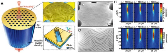
Figure 2. (a) Schematic of in-fiber metalens based on LAM-PCF. (b,c) SEM images of the fabricated PCF metalens with NA = 0.37. (d) Measured intensity distributions of PCF metalenses with NA = 0.37 and NA = 0.23. Reprinted with permission from Ref. [43]. Copyright 2019 De Gruyter.
By both experimental and computational simulation, the proposed LAM-PCF metalens with two different numerical apertures (NA) has demonstrated good focusing performance with focal lengths of 30 and 50 μm upon the incident RCP light at 1550 nm. Furthermore, the enhanced optical intensity has been found to be over 230% due to the tight and bright focusing spot (See Figure 2d). Following Yang’s work, in 2020, Korean researcher Kim et al. suggested that the PCF-based metallic metalens in [43] suffer from a low operation efficiency (~17%) due to the low polarization conversion efficiency and metal loss. As a result, Kim et al. proposed an all-dielectric metalens by depositing the aperiodic silicon (Si) nanopillars on top of the photonic crystal fiber [45]. The focusing effect was realized by tuning the diameters of Si nanopillars using the propagation phase. Simulation results have shown that the focusing efficiency of the dielectric PCF metalens has been improved to 88% with a focal length of 30 μm. Although the operating efficiency of the proposed PCF metalens has been enhanced, however, neither the newly designed fiber platform (the PCF type is the same as reported in [43]) nor the broadband focusing is presented in this work. In this regard, in 2021, Zhao et al. designed a customized all-glass PCF metalens for output guided beam focusing [46]. The schematic is shown in Figure 3a,b.
Figure 3. (a,b) Schematic of all-glass PCF metalens. Normalized intensity distribution of focal spots at x-z and x-y plane upon incident beam at the wavelength of (c,d) 800 nm, (e,f) 1300 nm, and (g,h) 1550 nm. Reprinted with permission from Ref. [46]. Copyright 2021 MDPI.
Zhao et al. replaced the air-holes constituting PCF cladding with fluorine-doped glass rods to reduce the refractive index between the core and cladding, which increased the single-mode operation regime. The designed LAM-PCF for loading the dielectric metalens has a large core diameter of 50 μm, which is twice as large than that used in [43][45][43,45]. The large core size supports more unit cells with higher resolution to tune the phase profile, and most importantly, allows for a larger focal length according to Equation (5). The 2π phase modulation was achieved by varying the diameters of TiO2 nanopillars using the propagation phase modulation method. Moreover, the author demonstrated a broadband focusing function with the designed LMA-PCF metalens covering the typical “three communication windows” (800–1550 nm), and the focusing performance with varying incident wavelengths has also been well studied. The simulated results have shown that the customized all-glass LMA-PCF could be operated in the broadband near-infrared range with a stably high focusing efficiency (~70%) and large focal length (~300 μm), which has greatly improved the focusing performance of in-fiber metalens. Besides the PCF as the substrate for integrating the flat metalens, single-mode fibers have also been selected as an appropriate candidate for saddling the metalenses to achieve the short or long-distance focusing of fiber guided mode in either visible band or the near-IR range [47][48][49][50][51][52][53][47,48,49,50,51,52,53], which is more approachable for the practical applications in the long-haul optical communication systems. Besides the extensive study of the focusing proprieties for this kind of fiber metalens, it has been found that the numerical aperture (NA) is also a key factor affecting the performance of optical since a larger NA supports a higher coupling efficiency of optical fiber to be applied to high-power applications. In this regard, the optical fiber metalens with the purpose of increasing the NA is also studied. Mostly recently, Matthias et al. proposed a model which combines the single-mode fiber with plasmonic metalens via a coreless glass section (expansion section, Figure 4a,b). By means of the insertion of the expansion section, the light propagating through the fiber end could be expanded to 48 μm and thus greatly enlarge the NA of the metalens (~0.3) [49]. In this application, the geometry phase method was applied, with gold nanoslits orientated to different angles to achieve the 2π phase profile indicated in Equation (5). The dimensions of the nanoslits were optimized using the Babinets’ principle to achieve the maximal transmission (T ~ 0.332) at the desired wavelength λ = 650 nm, resulting in L = 140 nm, W = 60 nm. This fiber metalens concept will find applications in a multitude of fields, including remote focusing, optical trapping, beam generation, and efficient light collection.
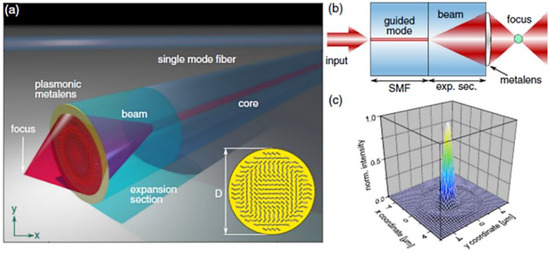
Figure 4. (a) Schematic of gold-coated plasmonic metasurface interfacing with single-mode step-index fiber. (b) Illustration of the interfacing structure including fiber expansion section. (c) Measured transverse intensity distribution of the focused spot in the focal plane. Reprinted with permission from Ref. [49]. Copyright 2021 WILEY-VCH.
In another practical application with light beam focusing, the fabricated fiber-integrated metalens was self-adapted and was directly applied to the laser lithography system for light beam routing [54]. The circular metalens, made of photoresist, has a phase profile defined by Equation (5), a focal length of 8 μm, and a near-infrared operating wavelength of 980 nm (See Figure 5a,b).
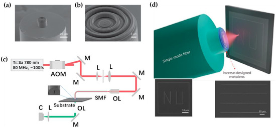
Figure 5. (a) SEM image of the fabricated metalens on top of the fiber core. (b) Enlarged view of the fiber meta-tip lens. (c) Schematic of the homemade two-photon laser writing system. (d) Illustration of two-photon writing process via fiber meta-tip lens and with the patterned “NU” and straight lines. Reprinted with permission from Ref. [54]. Copyright 2021 American Chemical Society.
The inverse-designed was fabricated via 3D direct-writing methodology [55]. The homemade fiber focusing metalens was employed as the objective lens and directly integrated into the two-photon laser writing system for sample patterning (Figure 5c,d). It has been demonstrated that the fiber meta-tip that incorporated two-photon laser writing setup has a better patterning resolution (~200 nm), as compared to the commercial direct laser writing system.
3.2. Function of Light Beam Routing
Apart from the light focusing function of optical fiber-integrated metalens, another typical functionality achieved by optical fiber-integrated metasurface is the light beam steering. This function is of great importance because it can not only flexibly control the propagation direction of the output beam, but it can also distinguish the incident beam with different chirality without the use of the bulky optical components (e.g., reflecting mirrors, wave-plates). It is worth mentioning that Maria et al. in 2017 first proposed the single-mode optical fiber meta-tip for beam steering (deflection) with the phase-gradient metasurface [56][57][56,57]. The proof-of-concept application was the beam steering of a transmitted beam by an arbitrary deflection angle. The deflection angle of the anomalous refraction, under normal incidence, can be derived from the generalized Snell’s law and Equation (1), which is expressed:

where α is the deflection angle, nfiber is the refractive index of the fiber, and γx is the phase gradient along the x direction in the metasurface plane. By means of Babinet-inverted plasmonic metasurfaces with tuning the rectangle nanoholes’ side lengths, the 2π phase coverage is achieved for the anomalous deflection beam [58]. The phase gradient can be calculated by:

where ΔΦ and lx represent the phase difference and distance between neighbor nanoholes. By varying the side lengths (L1 and L2) of the nanoholes according to the simulated “look-up” phase map, five prototypes of single-mode fiber-based metalens with varying phase gradients have been fabricated. Upon experimental verification, the anomalous beams with cross-polarization to the incident beam were deflected accordingly from 11° to 22°, as indicated by Equation (10), and the constructed fiber meta-tip prototype and beam deflection performance are depicted in Figure 6a–f.
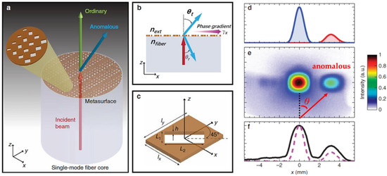
Figure 6. (a) Schematic of fiber meta-tip. (b) Illustration of generalized Snell’s law described in Equation (6). (c) Nanohole as the unit cell with 45° orientation in the x-y plane. (d) Simulated electric field-intensity profiles of fiber meta-tip 3 (γ = 14960 rad·cm−1). (e) Measured field-intensity map at z = 8 mm. (f) Transverse cuts at y = 0 comparing the measured (black-solid curve) and simulated (magenta-dashed curve) results. Reprinted with permission from Ref. [57]. Copyright 2017 Nature Publishing Group.
Following Maria’s work, in 2018, Michael et al. firstly proposed a UV curable polymer in-fiber polarimeter (see Figure 7a,b) with the template stripping transfer method [59][60][59,60]. The reason for using gold nanoholes as the unit cell is that the template stripping method could enhance the adhesion between metals (gold included) and silicon to ensure that the nanostructure pattern is smoothly transferred to the fiber core. The metasurface was made of two superimposed gratings of antenna columns arranged in a pattern where the antennas in each column are rotated 90° relative to antennas in the neighboring column, and the spacing between. The distance between the two columns is set as λ* (1 + 1/4) (λ is the resonant wavelength of the gold antenna) to scattering of polarization-dependent in-plane and out-plane grating orders. The out-plane order was scattered at an angle of 45° from the metasurface plane (λ = 1550 nm) and was used for polarization measurements. The authors have demonstrated the validity of the homemade in-fiber polarimeter since the measurement results of polarization states of the incident beam from the in-fiber polarimeter are almost identical to that of a commercial free-space polarimeter. The integration of in-line polarimeters represents an important step towards the miniaturization of optical polarimeter but is also useful for controlling light polarization in optical communication systems.
Figure 7. Micrograph images of patterned fibers. (a) Image of a polarimeter fabricated with the fiber exposure approach. (b) Image of a patterned fiber facet using the flood exposure approach, where a much larger area of nanoantennas arrays is transferred. Scale bar = 2 μm. Reprinted with permission from Ref. [59]. Copyright 2019 IEEE Photonics Society.
In addition to the beam deflection, the collimation of light beam has also been theoretically studied based on single-mode fiber (SMF600) metalens [61]. The key feature in this research is the use of low refractive index material (polymer, n = 1.52) to form the metalens to reduce the optical impedance match between the metasurface/fiber interface (see Figure 8a,b). More precisely, the elliptical nanopillars with uniform height but varied width and length (100–400 nm) constructed the metalens with 2π phase modulation (as described in Equation (5)), thus collimating the divergent beam output from the fiber end. It has been found that the highly divergent beam from the fiber facet can be tightly collimated with high efficiency of 95% while maintaining the Gaussian beam profile, and the concept of optical fiber metalens collimator may find applications in laser-delivery, biomedicine, and optical imaging.
Figure 8. Light propagation through the SMF without (a) metasurface on the facet and (b) with metalens to control the light beam convergence. Reprinted with permission from Ref. [61]. Copyright 2021 Optical Society of America.
In view of the abovementioned applications, it is evident that the combination of optical fiber with the superior light-guiding capability from the flat metasurface has provided an unprecedentedly well-established platform for the creation of novel photonic devices with complex functionalities at multiscale, which greatly advances the production of multiple photonic devices to be applied in diverse optical systems.