Your browser does not fully support modern features. Please upgrade for a smoother experience.
Please note this is a comparison between Version 1 by ADNAN ALI and Version 2 by Camila Xu.
Metamaterials are amongst the advanced materials made up initially with metal structures. However, there is a huge ongoing work on dielectric metasurfaces and metamaterials with the aim of replacing metal structures with dielectric ones in order to reduce the electromagnetic losses.
- metamaterial
- metasurface
- metadevice
- plasmonic
- nanoparticle
1. Introduction to Metamaterials
Metamaterials are amongst the advanced materials made up initially with metal structures. However, there is a huge ongoing work on dielectric metasurfaces and metamaterials with the aim of replacing metal structures with dielectric ones in order to reduce the electromagnetic losses.
Metamaterials’ physical properties rely mostly on their structures. In 1968, Veselago [1] explored materials of negative permittivity and permeability. Such characteristics though are not present in naturally found materials and can only be generated in metamaterials. During the electromagnetic wave transmission such as wave propagation, the effects generated by metamaterials can be clearly observed. Evolution of the topic of metamaterials with time is presented in Figure 1. From an applications point of view, metamaterials could be used in devices such as antennas [2], photonic filters [3], integrated network sensors [4] or new superlayers for the microwave and terahertz fields [5]. The deep understanding of metamaterials offers fullness of novel options ranging from laboratories concepts to practical engineering applications.
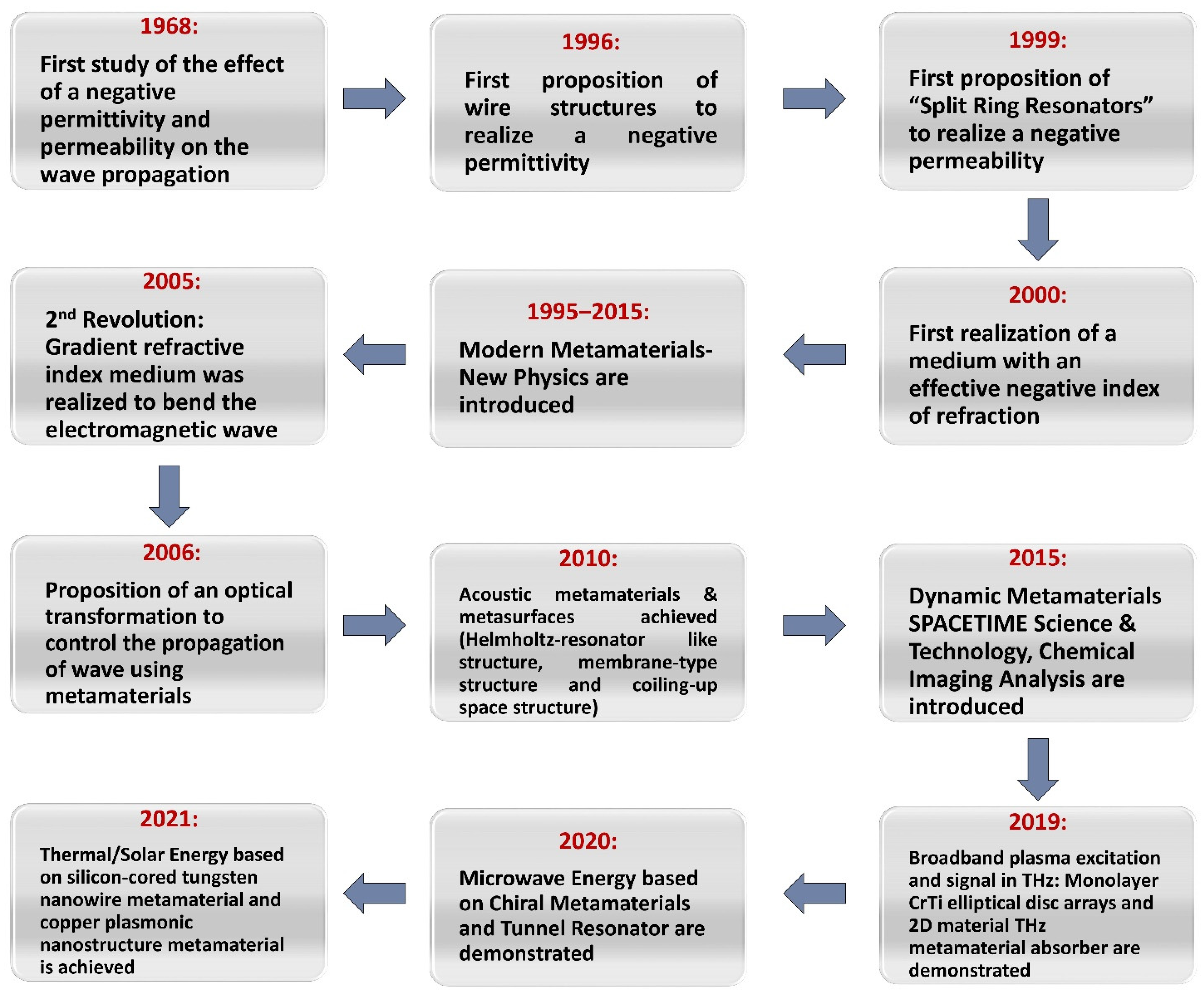
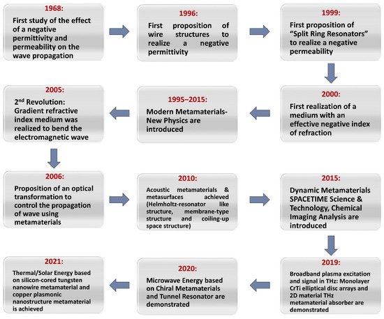
Figure 1. Schematic depicting the evolution of the field of metamaterials over the years, from 1968 to nowadays.
Schematic depicting the evolution of the field of metamaterials over the years, from 1968 to nowadays.
The term “metamaterial” comes from the Greek words “meta” and “material”, while “meta” refers to something that is beyond usual, rearranged, changed or innovative. It is an engineered material intended to attain unique properties and capabilities which are absent in natural materials. The term metamaterial is introduced by Walser in 1999 [6]. Metamaterial cannot be obtained from any continuous and homogenous medium, that is why the metamaterials are always of a composite nature. Usually, metamaterials are constructed from discrete resonant micro- and nanometer-scale objects which mimic the electromagnetic reaction of atoms and molecules of natural substances to make them interact with light and other forms of energy in specific controllable ways.
2. Evolution of Metamaterials
In 2019, Vicari et al. [7][24] modeled the growth of metamaterial-containing devices across eight different applications (displayed in Figure 23). The model looked at potential addressable markets based on various parameters including the cost, maturity and performance. It is based on inputs from a wide range of primary and secondary research. Vicari and his team explicitly seized the markets for metamaterial components in communications, sensing and acoustic applications. Many other applications are likely to appear and were grouped together into an “other” category. Market forecast for metamaterials is put at $10.7 billion by 2030. Through 2025, communications uses are by far the leading growth driver; however, by 2030, sensing uses grow to be the largest segment, reaching $5.5 billion compared to $4.4 billion in communications.


Metasurfaces
Depending on the materials employed and geometry, and per their frequency responses, metasurface-based device’s classification has been made as narrowband [3][11][3,27], broadband [12][13][14][28,29,30] and wideband [15][31]. Fano resonance is the typical case of narrowband application. The sharp resonance peak complemented by strong local field enhancement is amongst the most important aspects of Fano resonance [16][17][32,33]. It is the foundation of several practical applications such as nonlinear photonics and biological sensing. Metasurface dispersion for multiband and broadband applications can support super-resolution imaging beyond the diffraction limit, high-performance color filter, broadband absorbers and polarizers [15][18][19][20][31,34,35,36].
Metasurfaces are two-dimensional (2D) or planar versions of metamaterials dealing with subwavelength thickness [21][22][23][37,38,39]. Metasurfaces have unique abilities to block, absorb, concentrate, disperse or guide waves on the surface at a grazing incidence angle and in space at normal and oblique incidence, from microwave to visible frequencies. Surface waves can be well controlled by designing impedance cells to manipulate phase or group velocity [24][25][40,41]. These are patterned in such a way that may guide or separate waves in certain directions, and/or used to control scattering. By controlling the metasurface, unit cell sizes and shapes, multiple effective surface refractive indices can be achieved and different functions can be patterned on the surface. They can be used to design 2D microwave/optical lenses for antenna systems and planar microwave sources, such as Luneburg and fish-eye lenses [26][42].
The perspective of current implementation and growing metasurface and metadevice developments are shown in Figure 45. Different metasurfaces demonstrate different capabilities. The surface impedance can be modified and controlled by the structure of the cells that are widely applied to surface wave absorbers and surface waveguides. These metasurfaces also enable transmission and reflection to shape the beam.
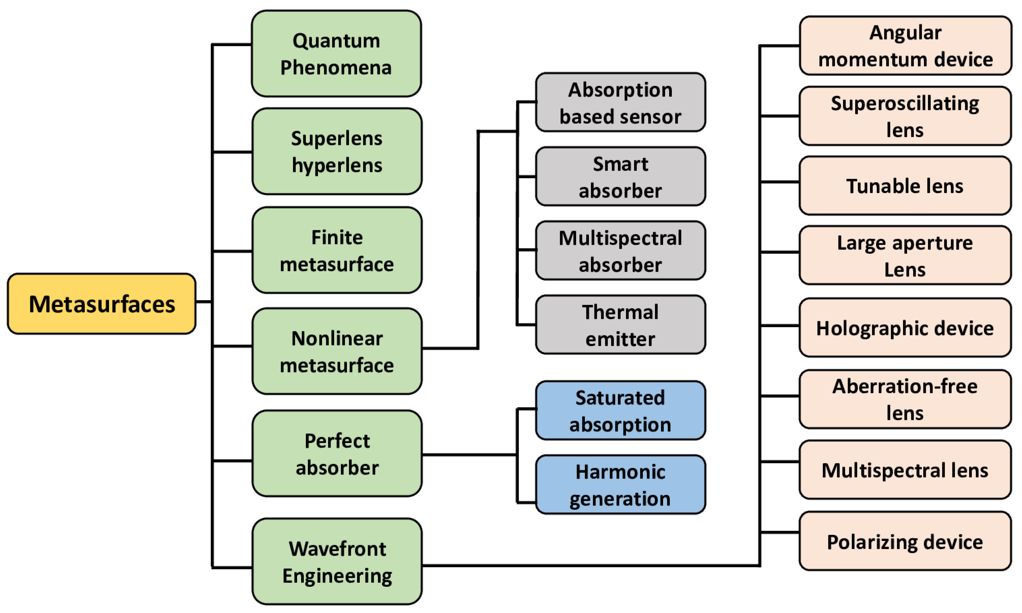
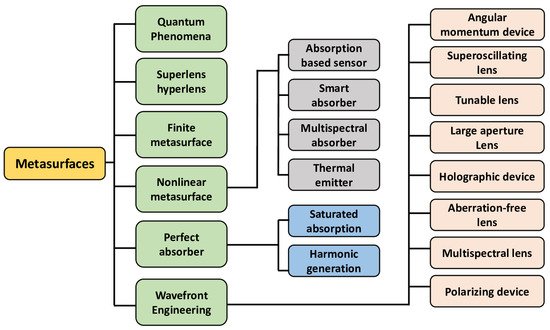
Figure 5. Chart summarizing the metasurfaces’ and metadevices’ applications.
Three-dimensional (3D) metamaterials, made often with periodic artificial materials composed of metals and/or dielectrics, have been widely studied owing to their unique interaction with electromagnetic waves that exceed the capabilities of naturally occurring or homogeneous materials [11][27][28][27,43,44]. Their exceptional ability to manipulate waves is due to their strong interaction with electrical and/or magnetic fields, typically provided by unit cell geometry-controlled resonant effects. These capabilities result in a broad range of applications such as antenna efficiency enhancement [29][30][45,46], ideal absorbers [31][32][33][47,48,49], superlenses [8][34][25,50], cloaking [35][36][37][51,52,53], elimination of scattering [12][38][28,54] and energy harvesting [39][40][41][16,55,56], among other applications in microwave and optical frequencies. When active and nonlinear components such as transistors [42][43][57,58], diodes [43][44][58,59], and varactors [45][46][47][60,61,62] are added to metasurfaces, novel tunability and switching abilities become possible.