Your browser does not fully support modern features. Please upgrade for a smoother experience.
Please note this is a comparison between Version 1 by Zhenzhen Kong and Version 3 by Dean Liu.
GeSn materials have attracted considerable attention for their tunable band structures and high carrier mobilities, which serve well for future photonic and electronic applications.GeSn 材料因其可调谐的能带结构和高载流子迁移率而引起了广泛关注,这为未来的光子和电子应用提供了很好的服务。
- GeSn growth
- selective etch
- strain modulation
- RPCVD
1. Introduction
一、简介
GeSn has aroused extensive attention as a result of its direct bandgap properties [1], compatibility with Si CMOS processes [2][3][4][5][6], higher absorption coefficients at short-wavelength infrared (SWIR) windows [7], and higher carrier mobilities compared with Si and Ge, etc. [3]. These characteristics show that GeSn materials will be promising for both optoelectronics and high-speed electronics for silicon photonic-electronic platforms in the near future. It is also expected that GeSn could open applications for thermoelectric materials in the near future [8][9]. There are several challenges in growing high quality GeSn: (I) the lattice mismatch between Ge and Sn is 14.7% and is even higher at 17% between Sn and Si; (II) incorporation of Sn in Ge is difficult due to the low solubility (<1%) of Sn in Ge and the instability of α-Sn above 13 °C; and (III) Sn precipitation and Sn agglomeration occur during growth. Therefore, growth tools, such as molecular beam epitaxy (MBE) [10][11][12], reduced pressure chemical vapor deposition (RPCVD) [13][14][15][16][17][18][19][20][21][22], ultra vacuum chemical vapor deposition (UHVCVD) [23], physical vapor deposition (PVD) [24], and sputtering technique [25][26] have been proposed to grow GeSn at low temperatures. Compared to MBE and PVD, CVD has the advantages of lower costs, higher growth rates, larger wafer sizes, and mass production potential which can easily be transferred to the Si-based microelectronic and photonic industry. As early as 2001, Kouvetakis’s group from Arizona State University (ASU) grew GeSn and GeSnSi via reactions of Si–Ge hydrides and SnD4 in a UHVCVD chamber, but SnD4 molecules are very unstable [27][28]. Then, in 2011, researchers from IMEC [14] and KTH proposed the growth of GeSn using commercially available reaction precursors (SnCl4/Ge2H6) in a production RPCVD tool [18]. Since then, many research groups reported the growth of GeSn using precursor combinations of SnCl4/Ge2H6 and SnCl4/GeH4 [13][14][15][16][17][18][19][20][21][22][23]. Moreover, GeSnSiC alloys were also grown using Si2H6, Ge2H6, SnCl4, and SiCH6, precursors which are also important for photonic applications [19][20]. From the mass production perspective, GeH4 is preferred to Ge2H6, owing to its wider usage and lower cost. In order to improve material properties, the effects of growth temperature, growth pressure, carrier gas, strain relaxation, and doping on GeSn growth were systematically investigated. Experimental results indicate that growth temperature, growth pressure, and strain relaxation were major factors towards achieving high Sn composition and high quality GeSn [29][30].GeSn 因其直接的带隙特性 [ 1 ] 、与 Si CMOS 工艺的兼容性[ 2、3、4、5、6 ]、在短波长红外 (SWIR) 窗口 [7] 的吸收系数较高而引起了广泛关注,和更高的载流子迁移率与 Si 和 Ge 等相比 [ 3 ]。这些特性表明,在不久的将来,GeSn 材料将在硅光子电子平台的光电子学和高速电子学方面大有前途。预计 GeSn 将在不久的将来打开热电材料的应用 [ 8 , 9 ]]。生长高质量的 GeSn 存在几个挑战: (I) Ge 和 Sn 之间的晶格失配为 14.7%,Sn 和 Si 之间的晶格失配甚至更高,达到 17%;(II) 由于 Sn 在 Ge 中的溶解度低 (<1%) 和 α-Sn 在 13 °C 以上的不稳定性, Sn 在 Ge 中的掺入很困难;(III)在生长过程中发生Sn析出和Sn聚集。因此,生长工具,例如分子束外延 (MBE) [ 10 , 11 , 12 ],减压化学气相沉积 (RPCVD) [ 13 , 14 , 15 , 16 , 17 , 18 , 19 , 20 , 21 , 22]、超真空化学气相沉积 (UHVCVD) [ 23 ]、物理气相沉积 (PVD) [ 24 ] 和溅射技术 [ 25 , 26 ] 已被提出在低温下生长 GeSn。与 MBE 和 PVD 相比,CVD 具有成本更低、生长速度更快、晶圆尺寸更大、量产潜力等优势,可以很容易地转移到硅基微电子和光子产业。早在 2001 年,来自亚利桑那州立大学 (ASU) 的 Kouvetakis 小组通过 Si-Ge 氢化物和 SnD 4 在 UHVCVD 室中的反应生长了 GeSn 和 GeSnSi,但 SnD 4 分子非常不稳定 [ 27 , 28]。然后,在 2011 年,来自 IMEC [ 14 ] 和 KTH 的研究人员提出了在生产 RPCVD 工具中使用市售反应前体 (SnCl 4 /Ge 2 H 6 ) 来生长 GeSn [ 18 ]。从那时起,许多研究小组报告了使用 SnCl 4 /Ge 2 H 6 和 SnCl 4 /GeH 4的前驱体组合来生长 GeSn [ 13 , 14 , 15 , 16 , 17 , 18 , 19 , 20 , 21 , 22, 23 ]。此外,GeSnSiC 合金还使用 Si 2 H 6、Ge 2 H 6、SnCl 4和 SiCH 6生长,这些前体对于光子应用也很重要 [ 19 , 20 ]。从量产角度看,GeH 4 优于 Ge 2 H 6,由于其使用范围更广,成本更低。为了改善材料性能,系统研究了生长温度、生长压力、载气、应变弛豫和掺杂对GeSn生长的影响。实验结果表明,生长温度、生长压力和应变松弛是实现高 Sn 成分和高质量 GeSn 的主要因素 [ 29 , 30 ]。
2. Growth Kinetics
. 生长动力学
The fundamental problem with growing GeSn layers is segregation of Sn atoms. There are two main factors which govern Sn segregation: chemical and size effects. The first effect depends on the heats of sublimation of Sn (65 kcal/mole) and Ge (89 kcal/mole), which in fact determine whether Sn-to-Sn or Sn-to-Ge bonding is favored. The size effect originates from the size difference between Sn and Ge atoms. Therefore, researchers may conclude that high incorporation of Sn in Ge is a real challenge as a result of both aforementioned effects.生长 GeSn 层的基本问题是 Sn 原子的偏析。控制 Sn 偏析的主要因素有两个:化学和尺寸效应。第一个影响取决于 Sn (65 kcal/mole) 和 Ge (89 kcal/mole) 的升华热,这实际上决定了 Sn-to-Sn 或 Sn-to-Ge 键合是有利的。尺寸效应源于Sn和Ge原子之间的尺寸差异。因此,我们可以得出结论,由于上述两种效应,在 Ge 中高掺入 Sn 是一个真正的挑战。 Prior to GeSn growth, a Ge buffer with a thickness of at least 1000 nm is necessary to be deposited for high quality epitaxy. The Ge buffer layer contains two layers which are grown at a temperature of 450 °C for the low layer, and at 650 °C for the cap layer. The first layer is highly defective; meanwhile, the second layer has significantly higher epitaxial quality. An annealing treatment at 850 °C ensures the defect density is minimized to a level of 107 cm−2. Since the main goal is to incorporate high Sn content in Ge, the quality of the buffer layer is very important. Figure 1 illustrates the series of grown samples. The amount of SnCl4 introduced into the epi chamber was increased in three steps of 0.8, 1, and 1.5 g/h. In these samples, Sn segregation appears as Sn dots on the surface of the GeSn layer. The sizes of the Sn dots depend on the thickness of the GeSn layer, and they become larger for thicker GeSn layers. Therefore, it is important in the characterization of GeSn layers that the presence of Sn dots not be misjudged as surface roughness, especially when they are small for thin GeSn layers. Since Sn atoms are large, and since the heat of sublimation for Sn is less than that for Ge, segregation of Sn in Ge buffer occurs from both chemical and size effects.在 GeSn 生长之前,需要沉积厚度至少为 1000 nm 的 Ge 缓冲层,以实现高质量的外延。Ge 缓冲层包含两层,底层在 450 °C 温度下生长,帽层在 650 °C 下生长。第一层缺陷严重;同时,第二层具有明显更高的外延质量。850℃的退火处理确保缺陷密度最小化到10 7 cm -2的水平。由于本研究的主要目标是在 Ge 中加入高 Sn 含量,因此缓冲层的质量非常重要。 图 3 说明了本研究中的一系列生长样品。SnCl 4的量 在 0.8、1 和 1.5 g/h 三个步骤中增加引入 Epi 室的量。在这些样品中,Sn 偏析表现为 GeSn 层表面上的 Sn 点。Sn 点的大小取决于 GeSn 层的厚度,并且对于更厚的 GeSn 层,它们变得更大。因此,在表征 GeSn 层时,重要的是不要将 Sn 点的存在误判为表面粗糙度,特别是当它们对于薄 GeSn 层来说很小时。由于 Sn 原子大,并且由于 Sn 的升华热小于 Ge 的升华热,因此 Ge 缓冲液中的 Sn 偏析发生在化学和尺寸效应上。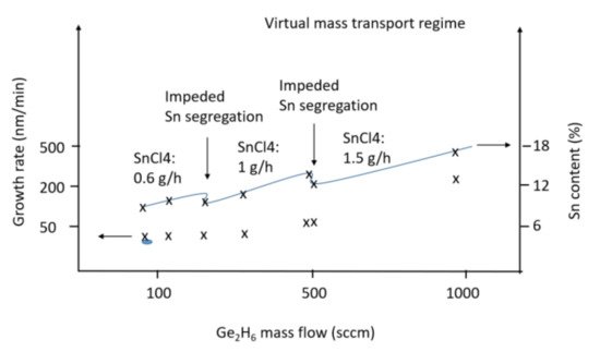
Figure 1. Growth parameters of GeSn deposition and its related Sn contents.
图 3 GeSn 沉积的生长参数及其相关的 Sn 含量。
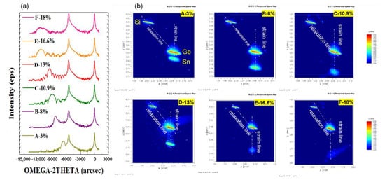
Figure 2. X-ray analysis of GeSn/Ge layers (a) rocking curves and (b) 224 HRRLMs.
图 4. GeSn/Ge 层的 X 射线分析 ( a ) 摇摆曲线和 ( b ) 224 HRRLM。
3. Strain Modulation of GeSnOI by Vertical Etching
3. 通过垂直蚀刻对 GeSnOI 的应变调制
The strain modulation of GeSnOI was studied by stepwise etching the Ge buffer. Figure 3 shows HRXRD results of as-grown and after 20 s, 100 s, and 120 s etching times of GeSnOI. In these experiments, the intensity of the Ge peak decreases gradually with increases in etching time, and later appears as Ge is completely etched away.通过逐步蚀刻 Ge 缓冲液研究了 GeSnOI 的应变调制。 图 10 显示了生长状态和 GeSnOI 蚀刻时间为 20 秒、100 秒和 120 秒后的 HRXRD 结果。在这些实验中,随着刻蚀时间的增加,Ge峰的强度逐渐减小,随后随着Ge被完全刻蚀掉而出现。
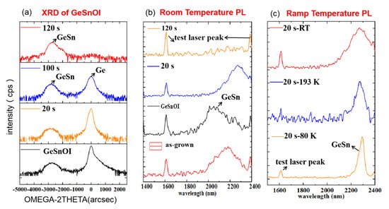
Figure 310. (a) XRD of GeSnOI as-grown (black line) and after wet etchings of 20 s (orange line), 100 s (blue line), and 120 s (red line); (b) PL at room temperature of GeSn as-grown (red line), GeSnOI (black line), and after wet etchings of 20 s (blue line), 100 s (amaranth line), and 120 s (orange line); and (c) PL of GeSnOI after wet etching of 20 s at temperatures of 80 K (orange line), 193 K (blue line), and room temperature (red line).
Figure 310b shows the GeSn peak has a blue-shift after the bonding process. It is believed that this shift is a result of the annealing treatment (300 °C 1 h) which could cause a number of Sn atoms to be pushed out from substitutional sites, resulting in strain reduction. This explanation originates from the fact that rwesearchers observed no defects in HRTEM results. Meanwhile, the etching of the Ge buffer creates a red-shift, as expected. The red-shift is caused by stress release and bandgap alignment in GeSn. Table 1 4 and Figure 310c demonstrate more PL investigation on the GeSnOI sample with a 20-s etching of Ge buffer at different temperatures. The PL peak’s FWHM at room temperature (shown as Table 14) is decreased at low temperature analysis, which is consistent with freezing of imperfections in the epilayer.
Table 14. PL data for the GeSn peak at 80 K and at room temperature (RT) after Ge vertical wet etching.
PL data for the GeSn peak at 80 K and at room temperature (RT) after Ge vertical wet etching.
| Sample | FWHM-80 K/nm | Peak of GeSn-80 K/nm | FWHM-RT/nm | Peak of GeSn-RT/nm |
|---|
Table 2. NBD results about GeSnOI strain before etching, and after wet etching for 20 s and 120 s.
表 5. 刻蚀前、湿法刻蚀 20 s 和 120 s 后 GeSnOI 应变的 NBD 结果。
| Sample样本 | Bulk Strain体应变 | Strain⊥(002)应变⊥ (002) | Strain//(220)应变// (220) | |
|---|---|---|---|---|
| GeSn Before bonding | -- | -- | 251 | 2166 |
| GeSnOI | ||||
| GeSnOI | 2.79% | 2.11% | 0.47% | |
| 129 | 2040 | 134 | 2039 | |
| 20 s | 60 | 2286 | 284 | 2270 |
| 120 s | 26 | 2279 | 345 | 2232 |
In order to find out the strain distribution in the above sample GeSnOI, NBD analysis was performed, as shown in Figure 411a–c, and more details about estimated strain values are demonstrated in Table 25. The strain is distributed at the top level in the middle of the GeSn layer and more relaxation occurs in the vertical direction close to the Ge buffer. No defects are created in GeSn layers, and by removing more Ge buffer the strain is constantly decreased.
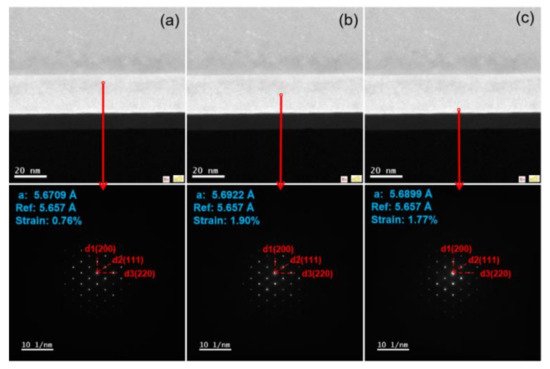
Figure 411. NBD in different GeSn regions of sample wet etched for 20 s; the reference is bulk Ge with lattice constant 5.657 Å. (a) Up; (b) middle; (c) down.
| 20 s | |||
| 20 秒 | 1.90% | 1.60 % | 0.17 % |
| 120 s120 秒 | 1.19% | 2.24% | −0.32% |