Dye-sensitized solar cells (DSSCs) have emerged as promising alternatives to traditional silicon-based solar cells due to their relatively high conversion efficiency, low cost, flexibility, and environmentally benign fabrication processes.
- active sites
- carbon
- dye-sensitized solar cells
- heteroatom dopants
- structural engineering
Definition:
Dye-sensitized solar cells (DSSCs) have emerged as promising alternatives to traditional silicon-based solar cells due to their relatively high conversion efficiency, low cost, flexibility, and environmentally benign fabrication processes.
1. Introduction
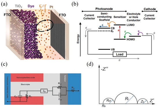
Dye-sensitized solar cells (DSSCs) have attracted much attention and have made increasing progress since they were first reported in 1991 [1]. Many attractive properties such as low-cost fabrication processes, lightweight, flexible, and good performance in weak light conditions have been demonstrated in DSSCs [2][3][4][2–4]. A DSSC consists of three main components: a dye-sensitized titania (TiO2) photoanode, the triiodide (I3–)/iodide (I–) electrolyte solution, and a platinum-coated fluorine-doped tin oxide (FTO) glass as a counter electrode (CE), as shown in Figure 1a [5]. Figure 1b briefly illustrates the energy diagram of a DSSC and the preferred charge transfer pathway.
When photons illuminate on adsorbed dye sensitizer, the electrons of dye were excited to lowest unoccupied molecular orbital (LUMO) as shown by the (a) in Figure 1b. Then the electrons were transferred into the conduction band (CB) of the semiconductors (b) and diffuse to the current collector (c). The electrons flow through the external circuit to the cathode (d) where the electrons transfer to the electrolyte (e) and the oxidized electrolyte (I3– ions) are reduced. The electrolyte (I– ions) can regenerate the oxidized dye (f). A circuit circle is completed.

Figure 1. (a) A schematic representation of a dye-sensitized solar cell (DSSC). (b) Energy diagram and desired electron pathway for a DSSC. CB and VB refer to the conduction band and valence band, respectively. EF represents the Fermi level of the semiconductor. LUMO and HOMO levels are the lowest unoccupied and highest unoccupied molecular orbitals of the sensitizer. Reprinted with permission from [5]. Copyright (2014) American Chemical Society.
2. Graphene-Based Counter Electrodes for DSSCs
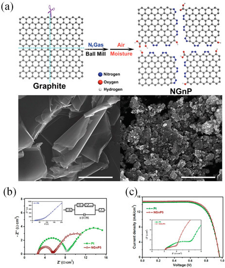
Many research groups have demonstrated that DSSCs with graphene CEs show the performances of DSSCs varied from 0.74% to 9.4% [6][7][8][9][10][11][12][13][14][15][16][17][37–48]. To the best of our knowledge, Xu and his coworkers were first to incorporate graphene materials as the catalytic CE for a DSSC [16][47]. The graphene sheets functionalized with 1-pyrenebutyrate (PB-G) were prepared by the reduction of graphene oxide. The conductivity of large-area flexible PB-G films exhibit seven orders of magnitude higher than that of the graphene oxide precursor. The efficiency of the DSSC with PB-G as a CE was measured to be 2.20%, compared to that of DSSC with standard Pt CE (3.98%). Graphene nanoplatelets (GnP) as a basic morphology of graphene have been prepared as the CE materials for DSSCs due to their large amount of active sites [18][19][20][49–51]. Ju et al. [21][14] prepared nitrogen-doped GNPs (NGnP) as metal-free electrocatalysts in DSSCs by ball-milling graphite in the presence of nitrogen gas (Figure 2a). The prepared NGnP show a structure of the nitrogen atom anchored at the edge of graphene nanoplatelets. The resultant NGnP CEs exhibited good electrocatalytic performance for the reduction of Co(bpy)33+, judging by the low charge-transfer resistance (Rct) values at the CE/electrolyte solution interface and high fill factor (71.9%) in DSSCs (Figure 2b). The performance of DSSCs with NGnP5 CE exhibited a PCE of up to 10.27%, which is higher than that of the DSSC with Pt-based CE (9.96%) (Figure 2c). Most importantly, the prepared NGnP CE exhibited superior stability compared to Pt CE by using the Co(bpy)32+/3+ redox couple. Where, the Co(bpy)32+/3+-based electrolytes not only provide higher voltage of DSSC, but also appear to be quite fast at carbon-based cathodes.

Figure 2. (a) A schematic illustration and SEM images of producing NGnP by the ball-milling graphite in the presence of nitrogen and subsequently exposing it to moisture in the air. (b) (top) Nyquist plot of electrochemical impedance spectrum (EIS) obtained from symmetrical dummy cells with the Pt/FTO and NGnP5/FTO electrodes. (bottom) Current–voltage characteristics of the DSSCs with the Pt and the NGnP5 CEs under AM1.5 illumination. (c) A table lists the photovoltaic parameters of the DSSCs with Pt and NGnP CEs [21][14]. Copyright 2014, WILEY-VCH.
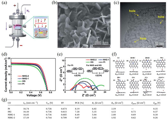
Structural engineering of graphene is an efficient route to increase the specific surface area and the number of active sites/defects. For example, Yang et al. [53] synthesized nitrogen-doped holey graphene (NHG) by chemical vapor deposition with MgO template and subsequently employing N2 plasma treatment (Figure 3a). High conductivity, large surface area and abundant edge-induced defects, and nitrogen dopants of NHG were obtained (Figure 3b,c), resulting in outstanding electrocatalytic activity for the I–/I3– redox reaction. The DSSCs with NHG CEs exhibited a higher PCE of 9.07% compared with that of DSSCs with Pt CEs (8.19%) (Figure 3d), which can be ascribed to the lower sheet resistance and Rct of NHG CEs (Figure 3e,g). Moreover, the detailed mechanism was further confirmed by density functional theory (DFT) calculations, which found that the pyridinic nitrogen (PN), pyrrolic nitrogen (PR), and edge-induced defects including five-carbon ring (C5) and seven-carbon ring (C7) act as catalytically active sites to greatly enhance the catalytic activity for the triiodide reduction reaction (Figure 3f).

Figure 3. (a) A schematic presentation of nitrogen-doped holey graphene (NHG) synthesis by N2 plasma treatment. A SEM image (b) and a high-resolution TEM image (c) of NHG. (d) Current-voltage characteristics of the DSSCs with different CEs. (e) EIS measurement and the corresponding equivalent circuits (inset). (f) The adsorption energy of I atom for various types of graphene structures. The gray, blue, brown, and white balls stand for carbon, nitrogen, iodine, and hydrogen atoms, respectively. (g) Photovoltaic parameters of DSSCs with different CEs and the resulting data from cyclic voltammetry and EIS. Reproduced from [22][53] with permission from the Royal Society of Chemistry.
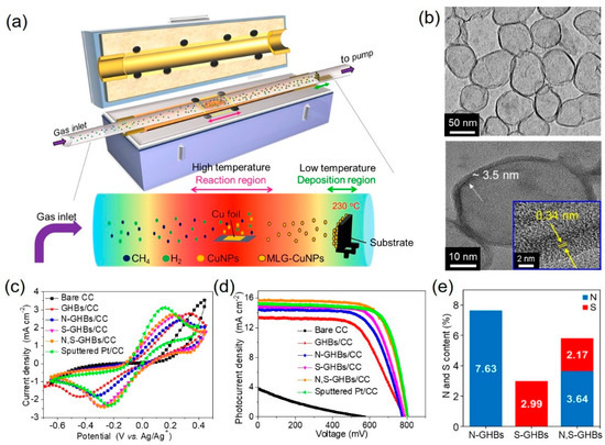
To further increase the catalytic activity, dual-doped graphene was also achieved by theoretical calculation and experimental results [23][24][25][26][55–58]. Chang et al. [27][59] synthesized nitrogen and sulfur co-doped graphene hollow nanoballs (N,S-GHBs) via chemical vapor deposition (CVD) as a CE for DSSCs (Figure 4a). The transmission electron microscopic images revealed the hollow structure of GHBs and confirmed the interlayer spacing (0.34 nm) of graphene (Figure 4b). Nitrogen doping improves the adsorption of I3– due to the electron transfer caused by the electronegativity differences between carbon and nitrogen atoms. On the other hand, sulfur-doping approach generates the geometric distortion due to the larger size of sulfur than carbon, which activates the sp2 bonding structure of carbon into unsaturated sp3 bonding structure. Among these doped GHB samples, N,S-GHBs show the best catalytic performance due to the synergistic effect from both electronic and geometric changes, caused by the N- and S-doping, respectively (Figure 4e). The DSSC with a N,S-GHB CE exhibits the PCE of 9.02%, comparable to that (8.90%) of a Pt-based counterpart due to the decrease of Rct for triiodide reduction reaction (Figure 4c,d and Table 1).

Figure 4. (a) A schematic illustration represents the growth of graphene hollow nanoballs (GHBs) on carbon cloth (CC) in a CVD reaction. (b) HR-TEM reveals the hollow structure and the lattice spacing of 0.34 nm of GHBs. (c) Cyclic voltammograms were tested with various CEs. (d) Photocurrent density vs. voltage curves of DSSCs with different CEs. (e) The doping amounts of the N and S atoms in N-GHBs/CC, S-GHBs/CC, and N,S-GHBs/CC are displayed for comparison [27][59]. Copyright 2020, Elsevier.
Table 1. The photovoltaic parameters of various CEs in a DSSC are compared under AM 1.5 G (100 mW cm−2) illumination [27][59].
| Counter Electrodes | η (%) |
VOC (mV) |
JSC (mA cm−2) |
FF | JIPCE (mA cm−2) |
|---|---|---|---|---|---|
| Bare CC | 0.48 ± 0.11 | 571 ± 2 | 4.33 ± 0.83 | 0.19 ± 0.01 | 4.14 |
| GHBs/CC | 6.20 ± 0.06 | 697 ± 5 | 14.50 ± 0.27 | 0.61 ± 0.01 | 14.29 |
| N-GHBs-P3/CC | 7.53 ± 0.06 | 703 ± 5 | 16.09 ± 0.18 | 0.67 ± 0.01 | 15.99 |
| Sputtered Pt/CC | 7.70 ± 0.14 | 735 ± 13 | 15.87 ± 0.32 | 0.66 ± 0.01 | 15.77 |
