Ball grid array (BGA) packaging is a new type of surface mount multi-terminal packaging technology. BGA packaging is widely used in the field of microelectronic manufacturing industries due to its multiple I/O volumes and excellent electric characteristics. However, due to environmental loads such as vibration and impact during its production and application, defects inevitably emerge in BGA solder joint defects, which will lead to the failure of electronic products.
1. Introduction
In recent years, with the development of consumers’ demand for electronic products, electronic products have displayed the trends of miniaturization, high performance, and high integration
[1][2][3][4][5][1,2,3,4,5]. Ball grid array (BGA) packaging overcomes the limitation of the number of I/O ports in the peripheral for wire bonding
[6][7][6,7]. The BGA chip is mounted on the carrier board through solder joints in the form of an array
[8][9][10][8,9,10]. This packaging technology not only expands the space of electronic devices but also greatly expands the number of I/O ports
[11]. Since it has the advantages of a high packaging density, high-speed signal processing, and low cost, BGA packaging has been widely applied in electronic industries
[12].
The BGA chip works in the environment and is inevitably by external loads, which are possibly caused by crashes or falls of the electronic product from a height
[13]. This results in the BGA chip malfunctioning and even failing, although its package plays the role of cushion protection and mechanical support. This is because the BGA solder joints are deformed and even damaged due to external loads
[14][15][16][17][18][14,15,16,17,18]. Therefore, analysis of mechanical properties and fatigue life prediction of BGA solder joints are hotspot studies in the field of electronic products’ reliability
[19][20][19,20].
2. Fatigue Failure Factors of BGA Solder Joints
Electronic products in real life work in a complex, changing environment, in which some environmental factors such as temperature, humidity, vibration, crashes, and dust affect their reliabilities
[21][22][21,22]. BGA solder joints, which have the functions of mounting
[23], electric connection
[24], protection
[25], heat dissipation
[21], and mechanical support
[26]. When BGA solder joints crash, this influences the reliability of BGA chips, and, further, the reliability of the electronic device
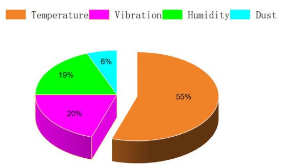
[21][27][21,27]. The U.S. Air Force Electronics Industry Department has reported that the failure of electronic components is mostly contributed by temperature changes, vibration and shock, moisture, and dust
[28][29][28,29], as illustrated in
Figure 1.

Figure 1. Factors affecting the failure of electronic components.
A large amount of heat is consequentially produced when the electronic components are working
[30]. If this heat cannot be effectively dissipated to the external environment, most of the heat will be concentrated in the electronic components to make the temperature inside the packaged chip rapidly rise, resulting in a burnout risk of the chip. If the temperature distribution inside the chip package is not uniform, the signal transmission characteristics of the chip will be influenced, thereby affecting the life and reliability of the electronic device. Additionally, because of the differences in the thermal expansion coefficient between chip packaging materials
[31][32][33][34][35][36][37][38][39][40][41][42][43][44][31,32,33,34,35,36,37,38,39,40,41,42,43,44], different materials have different degrees of thermal expansion and contraction under the influence of temperature. This results in additional stress and strain inside the electronic components, especially inside solder joints. This endless procedure will make the deformation large enough to result in the fatigue failure of the electronic device.
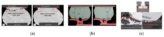
Figure 2a illustrates two SEM images of BGA solder joints with cracks due to the influence of the temperature
[21].
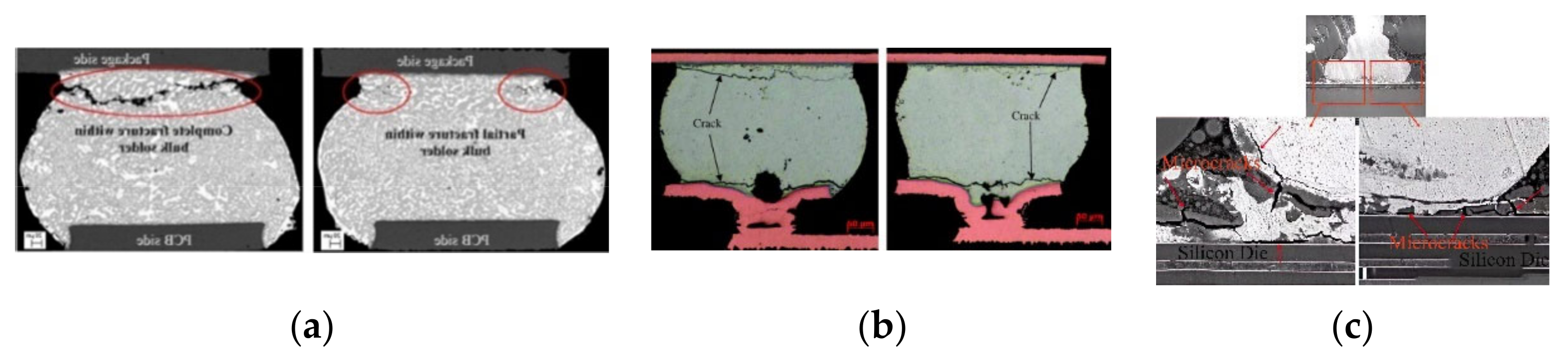
Figure 2. Failure of the solder joints of the BGA chips under the influences of (a) temperature, (b) vibration, and (c) humidity.
3. Research Methods for Fatigue Failure of BGA Solder Joints
The reliability of microelectronic packaging usually depends on the fatigue life of the solder joints
[45][54], which can be predicted by experimental observation and empirical mathematical models
[46][55].
Commonly, experimental studies require special experimental equipment and test samples to observe the process of cracking inside the BGA solder joint, which can be used to judge its failure
[47][56].
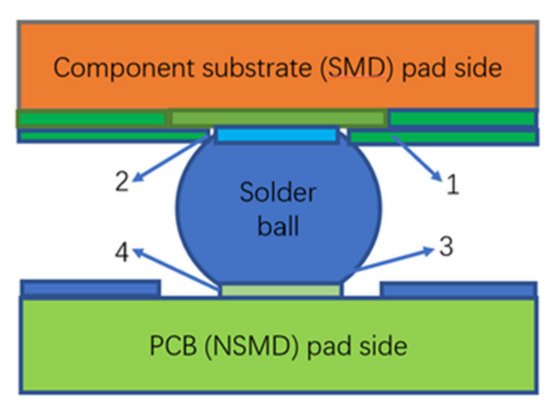
Figure 3 shows the main failure modes for BGA solder joints due to cracks
[48][57]. They are the fracture failures of the IMC layer on one side of the component, the solder joint neck, the IMC on the PCB side, and the junction of the PCB board and the pad. The test methods commonly used in experimental studies are summarized in
Table 12.
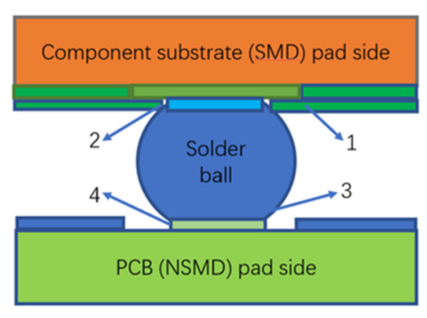
Figure 3. Main failure modes of BGA solder joints.
Table 12. Common test methods [47]. Common test methods [56].
| Test Methods |
Test Results |
Scopes of Application |
| White light interferometer |
Geometric size, displacement along the Z direction. Resolution: nanometer. |
Used at normal temperature. The sample surface is relatively flat. |
Electronic speckle interferometer
(ESPI) |
Three-direction displacement and deformation. Resolution: 20 nanometers. |
Temperature range for the experimental environment: −40~150, component level (including solder joints). |
| Moire interferometer |
In-plane displacement and deformation. Resolution: sub-pixel. |
Experimental test environment is the same as that for the ESPI. The iso-displacement line can be directly compared with the results obtained by the finite element simulation method. |
Digital image correlation
(DIC) |
In-plane displacement and deformation. Resolution: sub-pixel. |
Experimental test environment is the same as that for the ESPI. Large observation range (>cm to 1/10 pixel). It can be combined with a microscope and an SEM. |
| Silicon chip testing |
Stress and strain of the chip with the displacement. Resolution: MPa. |
Device-level test. Connected in the circuit. It can be applied to the field environment. |
| X-ray reflection |
Bending radius of crystal material (such as silicon material). |
Experimental environment temperature: −40~120. In principle, internal packaging and testing can be carried out. |
| X-ray diffraction |
Mechanical stress and strain of crystalline materials (such as silicon materials). |
Experimental environment temperature: −40~120. In principle, internal packaging and testing can be carried out. |
Scanning electron microscope
(SEM) |
In-plane displacement. Resolution: nanometer. |
While observing the morphology, the composition of the micro-area is analyzed. |
Another method is to use finite element simulation software to predict the fatigue life of solder joints [49][50][58,59]. Finite element software is employed to model and simulate the fatigue failure for specific components or solder joints under specific environmental parameters. Thus, significant information can be achieved, involving the stress and strain of key solder joints. Combined with the real working conditions of the packaging device, a suitable prediction model is selected to predict the fatigue life of the solder joint [46][55].
3.1. Research Methods for Fatigue Failure of BGA Solder Joints under Vibration Load
In commercial, industrial, and military applications, microelectronic devices often need to work under different vibration load conditions. Therefore, it is necessary to study the fatigue failure mechanism of BGA solder joints under vibration load
[51][52][62,63].
Fang Liu and Ye Lu
[53][64] et al. used a combination of finite element analysis and an experimental study to predict the fatigue life of BGA solder joints under random vibration loads. They used ABAQUS software to establish a three-dimensional finite element model of PCB components for random vibration simulation analysis. Then, the power density of the PCB components was obtained. Comparison experiments showed that the simulation results have a good correlation with the experimental results, which can validate the simulation model. Finally, the Miner rule and random vibration theory were used to determine the fatigue life of BGA solder joints under random vibration loads
[53][64].
3.2. Research Method for Fatigue Failure of Solder Joints under Thermal Stress
BGA solder joints are usually influenced by thermal shock loads when BGA-packaged devices are working, which reduces the mechanical strength of solder joints. If the mechanical strength decreases to a critical level, fatigue failure of the solder joint will occur
[21]. Driven by the thermal cycling, the difference in the thermal expansion coefficient between the BGA package and the PCB
[54][55][56][70,71,72], the alloy composition, and temperature changes in the solder joint matrix significantly affect the reliability of the solder joint
[25][32][25,32]. Thus, many studies have been performed on the fatigue failure of solder joints under thermal stress.
Vasu Vasudevan
[57][73] et al. experimentally studied the failure of 1295 solder joints in a BGA package. The thermal fatigue reliabilities of solder joints with different lead contents were analyzed under thermal stress by an accelerated temperature cycle test. They found that the reliability of the solder joints with a low lead content was low, and metallographic analysis showed that the solder joint failure occurred on the PCB side.
3.3. Research Method for Fatigue Failure of Solder Joints under Shear Stress
Electronic products will be subjected to high temperature and mechanical loads during normal operation. Since the thermal expansion coefficients of electronic components, intermetallic compounds, solders, and substrates are different, solder joints will be repeatedly subjected to periodic shear stress. Due to external forces, stress concentration will occur in the solder joints. If the load is large enough, solder joints are prone to shear fracture. Therefore, studying the failure mechanism of solder joints under shear force is important to improve the mechanical properties of solder joints
[58][76].
4. Several Common Models for Fatigue Life Prediction of Solder Joints
As the fatigue performance requirements of solder joints are becoming higher and higher, it is important to understand the differences in fatigue behavior under different mathematical models
[59][60][83,84]. Many researchers have proposed a number of fatigue failure models to study the reliabilities of solder joints
[61][62][85,86].
4.1. Coffin–Manson Life Model
The Coffin–Manson model is the earliest low-cycle fatigue model, proposed by L.F. Coffin and S. S. Manson in 1954
[63][87]. They pointed out that fatigue fracture was primarily caused by cyclic plastic strain of materials and solder joints
[64][88]. This model is a fatigue life prediction model based on plastic deformation. However, it ignores the influence of time and temperature on the life of solder joints
[65][89].
4.2. Darveaux Life Model
The Darveaux model utilizes the stress, strain, or energy between solder joints to characterize the relationship between their physical constants and their actual life under thermal or mechanical stress
[66][93]. The model divides the fatigue process into two stages, which are steady-state and nonlinear acceleration. In the first stage, the fatigue crack growth proceeds at a constant speed
[67][94]. In the second stage, the mechanical characteristics of the solder joint deteriorate sharply.
4.3. Paris Life Model
Paris proposed the famous Paris formula to demonstrate the principle of crack growth
[68][98], which is based on fracture mechanics. This formula combines fracture mechanics with fatigue life and provides a new direction for studying crack growth life
[69][99]. It uses the stress intensity factor to characterize the stress field intensity at the crack tip.
4.4. Creep Life Model
Creep is a phenomenon in which the strain of a solid material increases with the increase in the loading time under a constant external force. Early creep modeling was carried out by separating the elastic and plastic deformation mechanisms. The creep, plastic, elastic, and other deformations were overlapped to form the creep
[70][71][61,101], which is the main deformation failure mechanism of materials at high temperature. In particular, in microelectronic packaging, for example, for Sn-based lead-free solders, creep will occur when the operating temperature for the solder joint is 0.5 times more than the melting point of the solder
[72][102].
5. Conclusions
Research method: The research method should be established by combining finite element simulation technology and experimental verification. Board-level finite element simulation can be used for finite element simulation according to the actual situation. Different mesh densities can be divided for different key parts to improve the simulation efficiency and to obtain more accurate simulation results. Then, the dangerous solder joints of the chip can be located according to two simulation results, when the chip component is simulated. For the determination of the simulation load, the load coupling simulation method should be adopted according to the actual working environment of the components, which can closely simulate the actual working environment of the components. At the same time, the failure model should be purposively established for life prediction according to the chip failure mode and load conditions. Finally, the simulation analysis results should be compared with the experimental results achieved by the experimental verification, so as to modify the simulation model to improve its simulation accuracy. Thus, the fatigue life of solder joints can be obtained.
Characterization method: Traditional characterization methods observe surface appearances of solder joints, such as cracks and deformation, to determine the failure of solder joints, which will inevitably result in some errors. Thus, electrical performance tests, such as resistance measurements, combined with functional verification can be employed to determine whether the chip fails. This can improve the performance of the characterization method for solder joint failure.