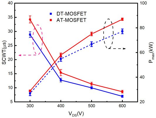
MOSFETs exhibit different failure modes at different DC bus voltages. For double trench SiC MOSFETs, the failure modes are gate fault at lower DC bus voltage and thermal runaway at higher DC bus voltage, while the failure modes for asymmetric trench SiC MOSFETs are soft failure and thermal runaway, respectively. The short-circuit withstand time (SCWT) of the asymmetric trench MOSFET is higher than that of the double trench MOSFET. The thermal and mechanical stresses inside the device during short-circuit test are simulated to explore the failure mechanism and reveal the impact of device structure on device reliability. Finally, a post-failure analysis was performed to verify the root cause of the equipment failure.
- SiC trench MOSFET
- short-circuit failure mechanism
- failure analysis
1. Introduction
/SiC surface roughness, and leads to local electric field concentration at the rough point. Hence, more charges are injected into the gate oxide, increases the charge through the gate oxide, shortening the time to dielectric breakdown [15][16]. Otherwise, threading dislocations (threading screw dislocations (TSDs) and threading edge dislocations (TEDs)) can cause significant leakage points in the device, which can severely degrade the performance of the SiC device [17][18]. The second issue is the infamous interface state problem. In addition, SiC devices tend to be operated under high voltage conditions, which makes the gate oxide layer bear a high electric field. In response, different shielding methods have been proposed, such as double trench MOSFETs (DT-MOSFETs) and asymmetric trench MOSFETs (AT-MOSFETs) [19][20]. The short-circuit failure modes of DT-MOSFETs have been reported in some detail [21][22], while the short-circuit reliability of AT-MOSFETs has been less studied. A comparison of the two devices’ short-circuit reliability has been reported [23], but it focuses more on the safe operating region and failure prediction regarding the device failure mode. The difference in the internal thermal and mechanical stress during the short-circuit process related to the difference in device structures has not been addressed.
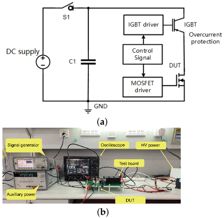
2. Device Structure and Experiment Setup
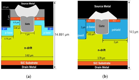
2.1. Device Structure

2.2. Experiment Setup
3. Experiment Results
3.1. DT-MOSFET
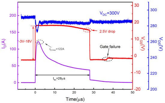
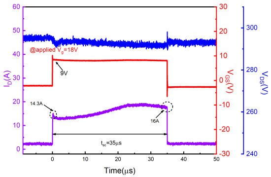
Figure 4 shows typical experimental short-circuit waveforms of SiC DT-MOSFETs with VDC = 300 V and VGS = 18 V/−3 V. When the device is turned on, internal parasitic parameters of the device and the test board cause a brief overshoot on VGS and VDS. However, this overshoot does not affect the following short-circuit process [26]. The short circuit pulse width tsc was gradually increased to 28 μs until the device reached the failure point, accompanied by a peak current value of 125 A and a VGS drop of 2.5 V. The anomaly only showed on the gate voltage waveform, manifested as a sudden increase of VGS (from −3 V to 0 V) after the device has been turned off for 7 μs, whereby the drain-source voltage still maintained to DC bus voltage. This means that the gate and source terminals are shorted, while the drain-source body diode still has blocking capability. The measured waveforms indicate the gate failure mode [10][27][28]. The same result was demonstrated in the subsequent electrical inspection of the three terminals, as shown in Table 2.

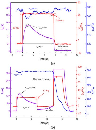
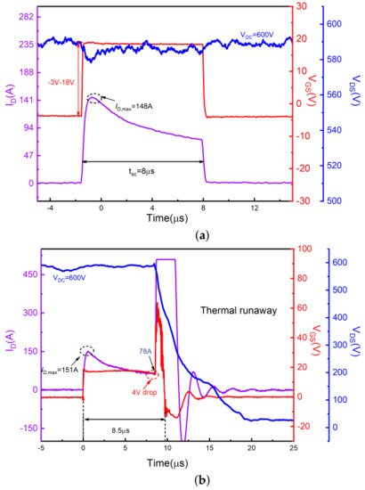
s. When the device fails, the peak current value is about 135 A, accompanied by the VGS drop of about 1 V. It can be seen from Figure 5b that a significant trail current appears after the device is turned off, climbing up to 39 A. High junction temperature caused by high power consumption can significantly increase the carrier density. Therefore, the device cannot be completely shut down at the end of short-circuit operation [29]. The hole current is the main cause of tail currents. Due to the existence of the tail current, more heat is generated, forming a positive feedback. If the tail current exceeds the threshold current to trigger the parasitic BJT, the hole density and the junction temperature will increase further and finally lead to thermal runaway [30]. As listed in Table 2, the resistance between the three terminals (RGS, RGD, and RDS) after the short-circuit test became quite low, revealing that all electrodes were shorted.
3.2. AT-MOSFET

References
- She, X.; Huang, A.Q.; Lucía, Ó.; Ozpineci, B. Review of silicon carbide power devices and their applications. IEEE Trans. Ind. Electron. 2017, 64, 8193–8205.
- Li, S.; Lu, S.; Mi, C.C. Revolution of Electric Vehicle Charging Technologies Accelerated by Wide Bandgap Devices. Proc. IEEE 2021, 109, 985–1003.
- Kumar, V.; Maan, A.S.; Akhtar, J. Barrier height inhomogeneities induced anomaly in thermal sensitivity of Ni/4H-SiC Schottky diode temperature sensor. J. Vac. Sci. Technol. B Nanotechnol. Microelectron. Mater. Process. Meas. Phenom. 2014, 32, 041203.
- Kumar, V.; Verma, J.; Maan, A.; Akhtar, J. Epitaxial 4H–SiC based Schottky diode temperature sensors in ultra-low current range. Vacuum 2020, 182, 109590.
- Cao, L.; Guo, Q.; Sheng, K. Comparative evaluation of the short circuit capability of SiC planar and trench power MOSFET. In Proceedings of the 2018 IEEE 2nd International Electrical and Energy Conference (CIEEC), Beijing, China, 4–6 November 2018; pp. 653–656.
- Cao, L.; Gao, Z.; Guo, Q.; Sheng, K. Experimental Investigations of SiC MOSFETs under Short-Circuit Operations. In Proceedings of the 2019 IEEE 31st International Symposium on Power Semiconductor Devices and ICs (ISPSD), Shanghai, China, 19–23 May 2019; pp. 227–230.
- Wang, Z.; Shi, X.; Tolbert, L.M.; Wang, F.; Liang, Z.; Costinett, D.; Blalock, B.J. Temperature-dependent short-circuit capability of silicon carbide power MOSFETs. IEEE Trans. Power Electron. 2015, 31, 1555–1566.
- Romano, G.; Maresca, L.; Riccio, M.; d’Alessandro, V.; Breglio, G.; Irace, A.; Fayyaz, A.; Castellazzi, A. Short-circuit failure mechanism of SiC power MOSFETs. In Proceedings of the 2015 IEEE 27th International Symposium on Power Semiconductor Devices & IC’s (ISPSD), Hong Kong, China, 10–14 May 2015; pp. 345–348.
- Boige, F.; Richardeau, F.; Trémouilles, D.; Lefebvre, S.; Guibaud, G. Investigation on damaged planar-oxide of 1200 V SiC power MOSFETs in non-destructive short-circuit operation. Microelectron. Reliab. 2017, 76, 500–506.
- Liu, J.; Zhang, G.; Wang, B.; Li, W.; Wang, J. Gate failure physics of SiC MOSFETs under short-circuit stress. IEEE Electron Device Lett. 2019, 41, 103–106.
- CREE. Discrete Silicon Carbide MOSFETs. 2011. Available online: https://www.wolfspeed.com/products/power/sic-mosfets (accessed on 4 January 2022).
- Nakamura, R.; Nakano, Y.; Aketa, M.; Noriaki, K.; Ino, K. 1200 V 4H-SiC trench devices. In Proceedings of the PCIM Europe 2014; International Exhibition and Conference for Power Electronics, Intelligent Motion, Renewable Energy and Energy Management, Nuremberg, Germany, 20–22 May 2014; VDE: Nuremberg, Germany, 2014; pp. 1–7.
- Baliga, B.J. Fundamentals of Power Semiconductor Devices; Springer Science & Business Media: Berlin, Germany, 2008.
- Nguyen, T.T.; Ahmed, A.; Thang, T.V.; Park, J.H. Gate Oxide Reliability Issues of SiC MOSFETs Under Short-Circuit Operation. IEEE Trans. Power Electron. 2015, 30, 2445–2455.
- Pappis, D.; Zacharias, P. Failure modes of planar and trench SiC MOSFETs under single and multiple short circuits conditions. In Proceedings of the 2017 IEEE 19th European Conference on Power Electronics and Applications (EPE’17 ECCE Europe), Warsaw, Poland, 11–14 September 2017; p. P.1.
- Kutsuki, K.; Murakami, Y.; Watanabe, Y.; Onishi, T.; Yamamoto, K.; Fujiwara, H.; Ito, T. Effect of surface roughness of trench sidewalls on electrical properties in 4H-SiC trench MOSFETs. Jpn. J. Appl. Phys. 2018, 57, 04FR02.
- Fiorenza, P.; Alessandrino, M.; Carbone, B.; Di Martino, C.; Russo, A.; Saggio, M.; Venuto, C.; Zanetti, E.; Giannazzo, F.; Roccaforte, F. Understanding the role of threading dislocations on 4H-SiC MOSFET breakdown under high temperature reverse bias stress. Nanotechnology 2020, 31, 125203.
- Claeys, C.; Simoen, E.; Put, S.; Giusi, G.; Crupi, F. Impact strain engineering on gate stack quality and reliability. Solid-State Electron. 2008, 52, 1115–1126.
- Nakamura, T.; Nakano, Y.; Aketa, M.; Nakamura, R.; Mitani, S.; Sakairi, H.; Yokotsuji, Y. High performance SiC trench devices with ultra-low ron. In Proceedings of the 2011 IEEE International Electron Devices Meeting, Washington, DC, USA, 5–7 December 2011; pp. 26.5.1–26.5.3.
- Peters, D.; Basler, T.; Zippelius, B.; Aichinger, T.; Bergner, W.; Esteve, R.; Kueck, D.; Siemieniec, R. The new CoolSiC™ trench MOSFET technology for low gate oxide stress and high performance. In Proceedings of the PCIM Europe 2017 International Exhibition and Conference for Power Electronics, Intelligent Motion, Renewable Energy and Energy Management, Nuremberg, Germany, 16–18 May 2017; VDE: Nuremberg, Germany, 2017; pp. 1–7.
- Wei, J.; Liu, S.; Tong, J.; Zhang, X.; Sun, W.; Huang, A.Q. Understanding Short-Circuit Failure Mechanism of Double-Trench SiC Power MOSFETs. IEEE Trans. Electron Devices 2020, 67, 5593–5599.
- Namai, M.; An, J.; Yano, H.; Iwamuro, N. Experimental and numerical demonstration and optimized methods for SiC trench MOSFET short-circuit capability. In Proceedings of the 2017 IEEE 29th International Symposium on Power Semiconductor Devices and IC’s (ISPSD), Sapporo, Japan, 28 May–1 June 2017; pp. 363–366.
- Deng, X.; Li, X.; Li, X.; Zhu, H.; Xu, X.; Wen, Y.; Sun, Y.; Chen, W.; Li, Z.; Zhang, B. Short-Circuit Capability Prediction and Failure Mode of Asymmetric and Double Trench SiC MOSFETs. IEEE Trans. Power Electron. 2020, 36, 8300–8307.
- ROHM. SCT3160KLGC11 Datasheet. 2018. Available online: https://fscdn.rohm.com/en/products/databook/datasheet/discrete/sic/mosfet/sct3160kl-e.pdf (accessed on 12 November 2021).
- Infineon. IMW120R090M1HXKSA1 Datasheet. 2020. Available online: https://www.infineon.com/dgdl/Infineon-IMW120R090M1H-DataSheet-v02_02-EN.pdf (accessed on 12 November 2021).
- Vishay. MKP1848C Datasheet. 2021. Available online: https://www.vishay.com/docs/26015/mkp1848cdclink.pdf (accessed on 4 January 2022).
- Onsemi. FGL40N120AN Datasheet. 2007. Available online: https://www.onsemi.com/products/discrete-power-modules/igbts/fgl40n120an (accessed on 4 January 2022).
- Wang, J.; Jiang, X.; Li, Z.; Shen, Z.J. Short-circuit ruggedness and failure mechanisms of Si/SiC hybrid switch. IEEE Trans. Power Electron. 2018, 34, 2771–2780.
- Sadik, D.P.; Colmenares, J.; Lim, J.K.; Bakowski, M.; Nee, H.P. Comparison of Thermal Stress During Short-Circuit in Different Types of 1.2-kV SiC Transistors Based on Experiments and Simulations. IEEE Trans. Ind. Electron. 2020, 68, 2608–2616.
- Peters, D.; Siemieniec, R.; Aichinger, T.; Basler, T.; Esteve, R.; Bergner, W.; Kueck, D. Performance and ruggedness of 1200V SiC—Trench—MOSFET. In Proceedings of the 2017 IEEE 29th International Symposium on Power Semiconductor Devices and IC’s (ISPSD), Sapporo, Japan, 28 May–1 June 2017; pp. 239–242.
- Romano, G.; Fayyaz, A.; Riccio, M.; Maresca, L.; Breglio, G.; Castellazzi, A.; Irace, A. A comprehensive study of short-circuit ruggedness of silicon carbide power MOSFETs. IEEE J. Emerg. Sel. Top. Power Electron. 2016, 4, 978–987.
- Riccio, M.; d’Alessandro, V.; Romano, G.; Maresca, L.; Breglio, G.; Irace, A. A temperature-dependent SPICE model of SiC Power MOSFETs for within and out-of-SOA simulations. IEEE Trans. Power Electron. 2017, 33, 8020–8029.
- Okawa, M.; Aiba, R.; Kanamori, T.; Yano, H.; Iwamuro, N.; Harada, S. Experimental and numerical investigations of short-circuit failure mechanisms for state-of-the-art 1.2 kV SiC trench MOSFETs. In Proceedings of the 2019 IEEE 31st International Symposium on Power Semiconductor Devices and ICs (ISPSD), Shanghai, China, 19–23 May 2019; pp. 167–170.