MOSFETs exhibit different failure modes at different DC bus voltages. For double trench SiC MOSFETs, the failure modes are gate fault at lower DC bus voltage and thermal runaway at higher DC bus voltage, while the failure modes for asymmetric trench SiC MOSFETs are soft failure and thermal runaway, respectively. The short-circuit withstand time (SCWT) of the asymmetric trench MOSFET is higher than that of the double trench MOSFET. The thermal and mechanical stresses inside the device during short-circuit test are simulated to explore the failure mechanism and reveal the impact of device structure on device reliability. Finally, a post-failure analysis was performed to verify the root cause of the equipment failure.
- SiC trench MOSFET
- short-circuit failure mechanism
- failure analysis
1.Introduction1. Introduction
Over the past few decades, wide-bandgap semiconductors like SiC have become more attractive compared to traditional silicon devices due to their high breakdown field,high thermal conductivity and wide bandgap\cite{she2017review,li2021revolution}. By now, SiC devices such as Schottky diodes have been rapidly developed and are widely used commercially [
2]. However, the short-circuit performance of SiC MOSFETs is still poor compared to Si-IGBTs. Due to their smaller area and higher power density, SiC MOSFETs have higher junction temperatures than Si-IGBTs and tend to suffer from thermal runaway [
6 ,
8]. In addition, the poorinterface state problem of SiC MOSFETs can also lead to gate reliability issues, causing the device gate failure[
As SiC material growth and device fabrication technologies have evolved, the structure of SiC MOSFETs has become increasingly sophisticated. Today, various commercial SiC MOSFETs with planar and trench gate structures from different manufacturers are available [11,12]. Compared to SiC planar gate MOSFETs, trench gate MOSFETs have higher power density, lower conduction resistance[
14]. First, the inhomogeneity of oxidation during gate formation makes the oxide thickness at the sidewall and trench bottom inconsistent. The oxidation inconsistency increases the SiO$_2$
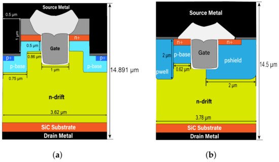
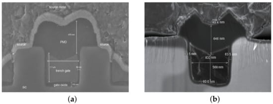
/SiC surface roughness, and leads to local electric field concentration at the rough point. Hence, more charges are injected into the gate oxide, increases the charge through the gate oxide, shortening the time to dielectric breakdown [15,16]. Otherwise, threading dislocations (threading screw dislocations (TSDs) and threading edge dislocations (TEDs)) can cause significant leakage points in the device, which can severely degrade the performance of the SiC device [17,18]. SThe second issue is the infamous interface state problem. In addition, SiC devices tend to be operated under high voltage conditions, which makes the gate oxide layer bear a high electric fields. In response, different shielding methods have been proposed, such as double trench MOSFETs (DT-MOSFETs) and asymmetric trench MOSFETs (AT-MOSFETs) [19,20]. The short-circuit failure modes of DT-MOSFETs have been reported in some detail [21,22], while the short-circuit reliability of AT-MOSFETs has been less studied. A comparison of the two devices’ short-circuit reliability has been reported [23], but it focuses more on the safe operating region and failure prediction regarding the device failure mode. The difference in the internal thermal and mechanical stress during the short-circuit process related to the difference in device structures has not been addressed.
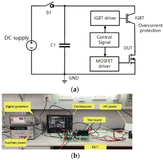
In this paper, the short-circuit ruggedness of two 1200V SiC trench MOSFETs with different gate oxide shielding methods(double-trench and asymmetric-trench) has been investigated. The device characteristics were recorded and analyzed. The maximum short-circuit withstand time(SCWT) of the devices have been measured and compared. To delve into the failure mechanism, the short-circuit process of the devices has been simulated by using a two-dimensional finite element numerical simulation tool. The distribution of currents, lattice temperatures, and mechanical stresses inside the devices were investigated in details. Finally, the failure was determined by using a failure analysis tool.
2. Device Structure and Experiment Setup
2. DEVICE STRUCTURE AND EXPERIMENT SETUP
2.1 DEVICE STRUCTURE2.1. Device Structure

2.2. Experiment Setup
3. Experiment Results
3.1. DT-MOSFET
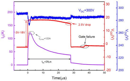
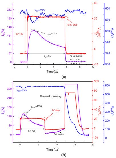
Figure 4 shows typical experimental short-circuit waveforms of SiC DT-MOSFETs with VDCDC = 300 V and VGSGS = 18 V/−3 V. When the device is turned on, internal parasitic parameters of the device and the test board cause a brief overshoot on VGS and VDS. However, this overshoot does not affect the following short-circuit process [28]. The short circuit pulse width tsc was gradually increased to 28 μs until the device reached the failure point, accompanied by a peak current value of 125 A and a VGSGS drop of 2.5 V. The anomaly only showed on the gate voltage waveform, manifested as a sudden increase of VGSGS (from −3 V to 0 V) after the device has been turned off for 7 μs, whereby the drain-source voltage still maintained to DC bus voltage. This means that the gate and source terminals are shorted, while the drain-source body diode still has blocking capability. The measured waveforms indicate the gate failure mode [10,29,30]. The same result was demonstrated in the subsequent electrical inspection of the three terminals, as shown in Table 2.

s. When the device fails, the peak current value is about 135 A, accompanied by the VGS drop of about 1 V. It can be seen from Figure 5b that a significant trail current appears after the device is turned off, climbing up to 39 A. High junction temperature caused by high power consumption can significantly increase the carrier density. Therefore, the device cannot be completely shut down at the end of short-circuit operation [31]. The hole current is the main cause of tail currents. Due to the existence of the tail current, more heat is generated, forming a positive feedback. If the tail current exceeds the threshold current to trigger the parasitic BJT, the hole density and the junction temperature will increase further and finally lead to thermal runaway [32]. As listed in Table 2, the resistance between the three terminals (RGSGS, RGDGD, and RDS) after the short-circuit test became quite low, revealing that all electrodes were shorted.
DS) after the short-circuit test became quite low, revealing that all electrodes were shorted.
3.2. AT-MOSFET
Figure 6 shows typical experimental short-circuit waveforms of SiC AT-MOSFETs at 300 V DC bus voltages, and gate bias was set as VGS = 18 V/−3 V. Under the same conditions, the SiC AT-MOSFET shows better short-circuit performance than the DT-MOSFET (35 μs for AT-MOSFET, 28 μs for DT-MOSFET). Under the same conditions, the SiC AT-MOSFET shows better short-circuit performance than the DT-MOSFET (35 μs for AT-MOSFET, 28 μs for DT-MOSFET). However, the longer short-circuit time leads to more serious device damage. After withstanding a 35 μs short-circuit pulse, the device is no longer able to operate normally. First, the short-circuit current drops to a dozen amps and shows an abnormal upward trend. In addition, the gate voltage is 9 V/−2 V even external 18 V/−3 V is applied. This indicates that a leakage path is formed between the gate and source, but they are not completely shorted, which is referred to as the soft failure. Devices have been previously reported to fail at low bus voltages due to gate-source SiO2
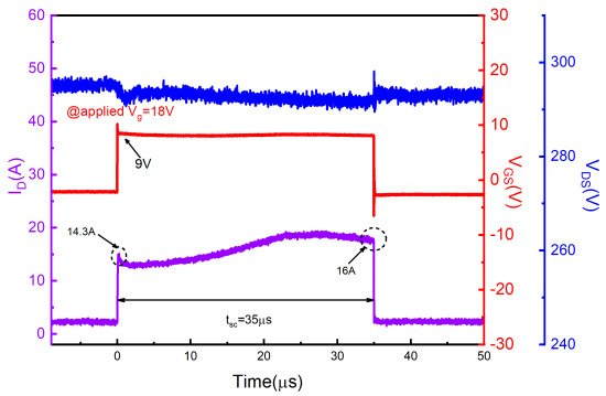


Figure 7 shows short-circuit waveforms of SiC AT-MOSFETs at 600 V DC bus voltages, and gate bias was set as VGS = 18 V/−3 V. At higher bus voltage, the device is subjected to higher power dissipation and the AT-MOSFET exhibits a thermal runaway mode after a 8.5 μs SC pulse. At higher bus voltage, the device is subjected to higher power dissipation and the AT-MOSFET exhibits a thermal runaway mode after a 8.5 μs SC pulse. The performance is slightly better than that of DT-MOSFETs, but it is somewhat different from the thermal runaway mode of DT-MOSFETs. First, the thermal runaway of the AT-MOSFETs does not occur after the device is turned off, but during the period when the short-circuit stress is applied. A comparison with the last waveforms measured before failure shows that the current increases during the short-circuit pulse. For example, the drain current increased from 66 A to 78 A at 7 μs. This indicates that a trailing current has occurred during the short-circuit pulse. As the junction temperature increases further, the current value is sufficient to trigger the parasitic BJT before the device shuts down. Compared to the DT-MOSFETs, the higher power level of the AT-MOSFET results in a higher peak current than the DT-MOSFETs, making the junction temperature rise faster, thus causing the thermal runaway mode to be triggered before the device is turned off. The second point is that the gate-source voltage of the AT-MOSFETs exhibites anomalies during the short-circuit pulse. There is a gate voltage drop of about 4 V near the point of failure, indicating that a high leakage current is flowing across the gate resistance. This indicates that the gate degradation occurs also. However, the junction temperature rises rapidly due to the higher bus voltage, so that there is not enough time for the gate to be damaged seriously before the thermal runaway occurs. The electrical characteristics in Table 3 also shows that all three terminals of the device are shorted together.
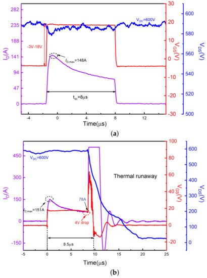
waveforms measured before failure and (b) at failure.
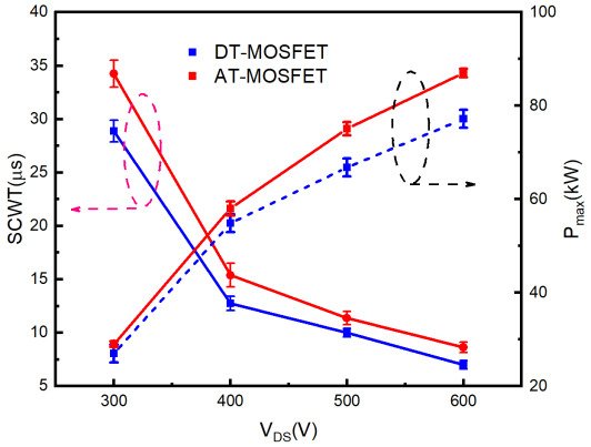
Figure 8.
