MOSFET 在不同的直流总线电压下表现出不同的故障模式。对于双沟槽 SiC MOSFET,故障模式是较低直流总线电压下的栅极故障和较高直流总线电压下的热失控,而非对称沟槽 SiC MOSFET 的故障模式分别是软故障和热失控。非对称沟槽 MOSFET 的短路耐受时间 (SCWT) 高于双沟槽 MOSFET。对短路测试期间器件内部的热应力和机械应力进行了模拟,以探究故障机制并揭示器件结构对器件可靠性的影响。最后,进行了故障后分析,验证了设备故障的根本原因。 MOSFETs exhibit different failure modes at different DC bus voltages. For double trench SiC MOSFETs, the failure modes are gate fault at lower DC bus voltage and thermal runaway at higher DC bus voltage, while the failure modes for asymmetric trench SiC MOSFETs are soft failure and thermal runaway, respectively. The short-circuit withstand time (SCWT) of the asymmetric trench MOSFET is higher than that of the double trench MOSFET. The thermal and mechanical stresses inside the device during short-circuit test are simulated to explore the failure mechanism and reveal the impact of device structure on device reliability. Finally, a post-failure analysis was performed to verify the root cause of the equipment failure.
- SiC trench MOSFET
- short-circuit failure mechanism
- failure analysis
一、简介
Over the past few decades, wide-bandgap semiconductors like SiC have become more attractive compared to traditional silicon devices due to their high breakdown field,high thermal conductivity and wide bandgap\cite{she2017review,li2021revolution}. By now, SiC devices such as Schottky diodes have been rapidly developed and are widely used commercially [1,2]. However, the short-circuit performance of SiC MOSFETs is still poor compared to Si-IGBTs. Due to their smaller area and higher power density, SiC MOSFETs have higher junction temperatures than Si-IGBTs and tend to suffer from thermal runaway [5,6 ,7,8]. In addition, the poorinterface state problem of SiC MOSFETs can also lead to gate reliability issues, causing the device gate failure[9,10].
As SiC material growth and device fabrication technologies have evolved, the structure of SiC MOSFETs has become increasingly sophisticated. Today, various commercial SiC MOSFETs with planar and trench gate structures from different manufacturers are available [11,12]. Compared to SiC planar gate MOSFETs, trench gate MOSFETs have higher power density, lower conduction resistance[13]. Although SiC trench MOSFETs have many advantages, their reliability needs further research due to the defects introduced during manufacturing process [14]. First, the inhomogeneity of oxidation during gate formation makes the oxide thickness at the sidewall and trench bottom inconsistent. The oxidation inconsistency increases the SiO$_2$/SiC surface roughness, and leads to local electric field concentration at the rough point. Hence, more charges are injected into the gate oxide, increases the charge through the gate oxide, shortening the time to dielectric breakdown[15,16].Otherwise, threading dislocations (threading screw dislocations (TSDs) and threading edge dislocations (TEDs)) can cause significant leakage points in the device, which can severely degrade the performance of the SiC device[17,18]. Second issue is the infamous interface state problem. In addition, SiC devices tend to be operated under high voltage conditions, which makes the gate oxide layer bear a high electric fields. In response, different shielding methods have been proposed, such as double trench MOSFETs (DT-MOSFETs) and asymmetric trench MOSFETs(AT-MOSFETs)[19,20]. The short-circuit failure modes of DT-MOSFETs have been reported in some detail[21,22], while the short-circuit reliability of AT-MOSFETs has been less studied. A comparison of the two devices’ short-circuit reliability has been reported[23], but it focuses more on the safe operating region and failure prediction regarding the device failure mode. The difference in the internal thermal and mechanical stress during the short-circuit process related to the difference in device structures has not been addressed.
In this paper, the short-circuit ruggedness of two 1200V SiC trench MOSFETs with different gate oxide shielding methods(double-trench and asymmetric-trench) has been investigated. The device characteristics were recorded and analyzed. The maximum short-circuit withstand time(SCWT) of the devices have been measured and compared. To delve into the failure mechanism, the short-circuit process of the devices has been simulated by using a two-dimensional finite element numerical simulation tool. The distribution of currents, lattice temperatures, and mechanical stresses inside the devices were investigated in details. Finally, the failure was determined by using a failure analysis tool.
2. MOSFDET 的短路性能仍然较差。由于其更小的面积和更高的功率密度,SiVIC MOSFET 具有比 Si-IGBT 更高的结温,并且容易遭受热失控 [ 5 , 6 , 7 , 8]。此外,Si STRUC MOSFET 的界面态较差问题也会导致栅极可靠性问题,从而导致器件栅极失效 [ 9 , 10 ]。
UP
/SiC 表面粗糙度,并导致粗糙点处局部电场集中。因此,更多的电荷注入到栅氧化层,增加了通过栅氧化层的电荷,缩短了介质击穿的时间[ .15 , 16 ]。否则,螺纹位错(螺纹位错 (TSDs) 和螺纹刃位错 (TEDs))会导致器件中出现明显的泄漏点,从而严重降低 SiC 器件的性能 [ 17 , 18]。第二个问题是臭名昭著的接口状态问题。此外,SiC器件往往工作在高电压条件下,这使得栅氧化层承受高电场。作为回应,已经提出了不同的屏蔽方法,例如双沟槽 MOSFVICET (DT-MOSFET) 和非对称沟槽 MOSFET (AT-MOSFET) [ 19 , 20 ]。DT-MOSFSTRUCTURET 的短路故障模式已被详细报道 [ 21 , 22 ],而 AT-MOSFET 的短路可靠性研究较少。已经报道了两种器件的短路可靠性比较[ 23],但更侧重于设备故障模式的安全工作区域和故障预测。与器件结构差异相关的短路过程中内部热应力和机械应力的差异尚未得到解决。
2. 设备结构和实验设置
2.1。设备结构
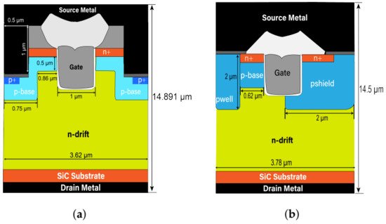
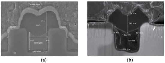

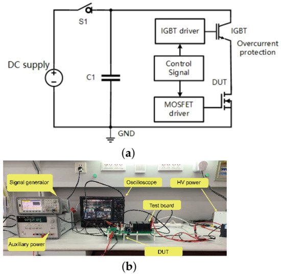
2.2. Experiment Setup
3. Experiment Results
3.1. DT-MOSFET
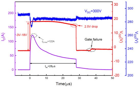
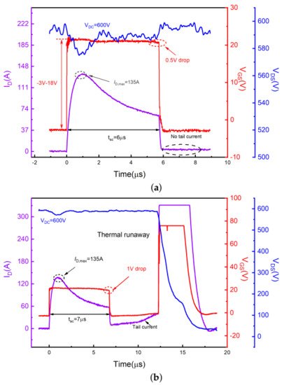
Figure 4 shows typical experimental short-circuit waveforms of SiC DT-MOSFETs with VDC = 300 V and VGS = 18 V/−3 V. When the device is turned on, internal parasitic parameters of the device and the test board cause a brief overshoot on VGS and VDS. However, this overshoot does not affect the following short-circuit process [28]. The short circuit pulse width tsc was gradually increased to 28 μs until the device reached the failure point, accompanied by a peak current value of 125 A and a VGS drop of 2.5 V. The anomaly only showed on the gate voltage waveform, manifested as a sudden increase of VGS (from −3 V to 0 V) after the device has been turned off for 7 μs, whereby the drain-source voltage still maintained to DC bus voltage. This means that the gate and source terminals are shorted, while the drain-source body diode still has blocking capability. The measured waveforms indicate the gate failure mode[10,29,30]. The same result was demonstrated in the subsequent electrical inspection of the three terminals, as shown in Table 2.

s. When the device fails, the peak current value is about 135 A, accompanied by the VGS drop of about 1 V. It can be seen from Figure 5b that a significant trail current appears after the device is turned off, climbing up to 39 A. High junction temperature caused by high power consumption can significantly increase the carrier density. Therefore, the device cannot be completely shut down at the end of short-circuit operation [31]. The hole current is the main cause of tail currents. Due to the existence of the tail current, more heat is generated, forming a positive feedback. If the tail current exceeds the threshold current to trigger the parasitic BJT, the hole density and the junction temperature will increase further and finally lead to thermal runaway [32]. As listed in Table 2, the resistance between the three terminals (RGS, RGD, and RDS) after the short-circuit test became quite low, revealing that all electrodes were shorted.
3.2. AT-MOSFET
Figure 6 shows typical experimental short-circuit waveforms of SiC AT-MOSFETs at 300 V DC bus voltages, and gate bias was set as VGS = 18 V/−3 V. Under the same conditions, the SiC AT-MOSFET shows better short-circuit performance than the DT-MOSFET (35 μs for AT-MOSFET, 28 μs for DT-MOSFET). Under the same conditions, the SiC AT-MOSFET shows better short-circuit performance than the DT-MOSFET (35 μs for AT-MOSFET, 28 μs for DT-MOSFET). However, the longer short-circuit time leads to more serious device damage. After withstanding a 35 μs short-circuit pulse, the device is no longer able to operate normally. First, the short-circuit current drops to a dozen amps and shows an abnormal upward trend. In addition, the gate voltage is 9 V/−2 V even external 18 V/−3 V is applied. This indicates that a leakage path is formed between the gate and source, but they are not completely shorted, which is referred to as the soft failure. Devices have been previously reported to fail at low bus voltages due to gate-source SiO2
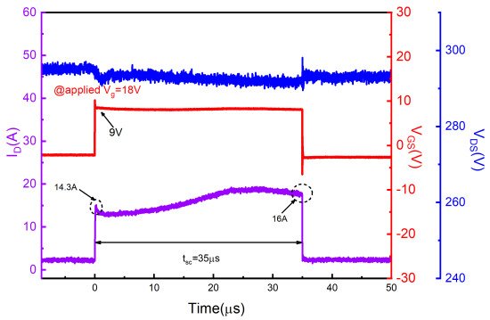

Figure 7 shows short-circuit waveforms of SiC AT-MOSFETs at 600 V DC bus voltages, and gate bias was set as VGS = 18 V/−3 V. At higher bus voltage, the device is subjected to higher power dissipation and the AT-MOSFET exhibits a thermal runaway mode after a 8.5 μs SC pulse. At higher bus voltage, the device is subjected to higher power dissipation and the AT-MOSFET exhibits a thermal runaway mode after a 8.5 μs SC pulse. The performance is slightly better than that of DT-MOSFETs, but it is somewhat different from the thermal runaway mode of DT-MOSFETs. First, the thermal runaway of the AT-MOSFETs does not occur after the device is turned off, but during the period when the short-circuit stress is applied. A comparison with the last waveforms measured before failure shows that the current increases during the short-circuit pulse. For example, the drain current increased from 66 A to 78 A at 7 μs. This indicates that a trailing current has occurred during the short-circuit pulse. As the junction temperature increases further, the current value is sufficient to trigger the parasitic BJT before the device shuts down. Compared to the DT-MOSFETs, the higher power level of the AT-MOSFET results in a higher peak current than the DT-MOSFETs, making the junction temperature rise faster, thus causing the thermal runaway mode to be triggered before the device is turned off. The second point is that the gate-source voltage of the AT-MOSFETs exhibites anomalies during the short-circuit pulse. There is a gate voltage drop of about 4 V near the point of failure, indicating that a high leakage current is flowing across the gate resistance. This indicates that the gate degradation occurs also. However, the junction temperature rises rapidly due to the higher bus voltage, so that there is not enough time for the gate to be damaged seriously before the thermal runaway occurs. The electrical characteristics in Table 3 also shows that all three terminals of the 表 3还显示器件的所有三个端子都短接在一起。device are shorted together.
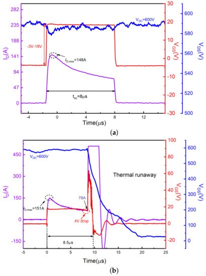
waveforms measured before failure and (b) at failure.
The 7.results 600 Vof DC 总线电压下 SiC AT-MOSFET 的短路波形。(SCWT and extracted Pmax ) 故障前测量的最后波形和 (comparison between DUTs bare )shown 故障时测量的波形。
SCWTin 的结果和Figure 8. DUT 之间的提取 Pmax 比较如图he maximum power dissipated in the short-circuit test is higher because 8所示。短路测试中消耗的最大功率更高,因为the AT-MOSFETs has 的额定电流高于a higher current rating than the DT-MOSFET。但s. However, the survival time of DT-MOSFET在不同母线电压下的存活时间比s at different bus voltages are shorter than that of AT-MOSFET短,有待进一步研究。s, which needs further study.
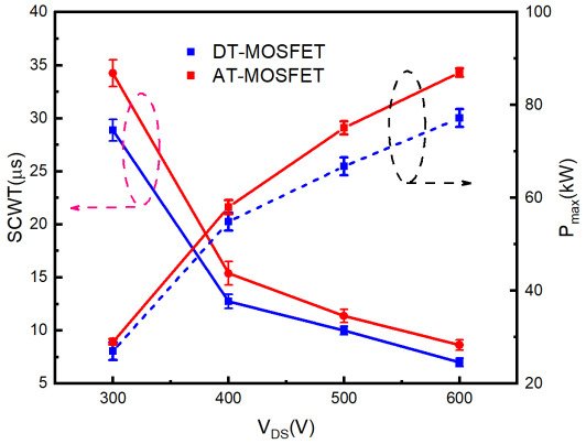
图 8.不同 DUT 在不同条件下的SCWT 和提取的Pmax比较。Figure 8. SCWT and Extracted Pmax comparison of different DUTs under different conditions.
