Graphene—a two-dimensional allotrope of carbon in a single-layer honeycomb lattice nanostructure—has several distinctive optoelectronic properties that are highly desirable in advanced optical communication systems. Meanwhile, silicon photonics is a promising solution for the next-generation integrated photonics, owing to its low cost, low propagation loss and compatibility with CMOS fabrication processes.
- graphene
- silicon photonics
- optics communications
1. Introduction
2. Physical Properties and Hybrid Graphene/Silicon Fabrication Processes
3. High-Performance Modulation Devices Based on Graphene
4. High-Performance Photodetector Based on Graphene
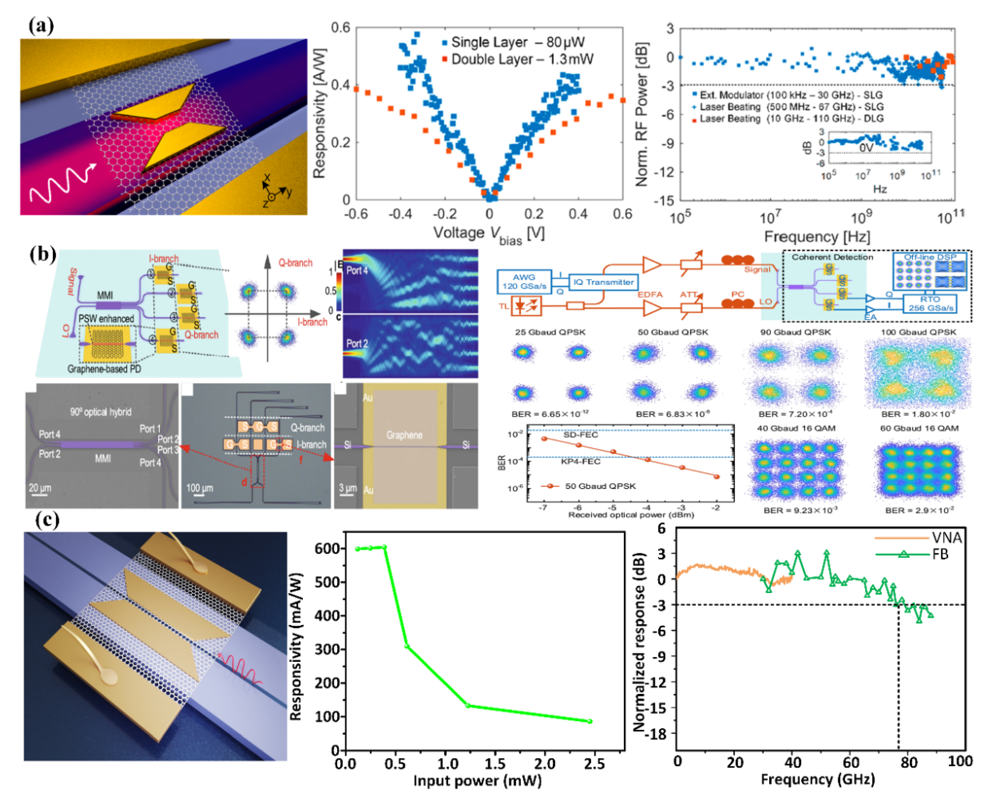
Due to its transparency in the telecommunications C-band near 1550 nm, silicon is inefficient in converting light into an electrical signal. Up to now, the mainstream of integrated photodetectors in silicon photonics for the communication wavelengths includes employing germanium (Ge) or monolayer graphene as photodetection material [53,54][24][25]. Ge-Si hybrid photodetectors have been widely studied and reached significant maturity thanks to their ability to absorb light in the telecommunications band near 1550 nm. High responsivity larger than 1 A/W has been achieved and an impressive bandwidth of 265 GHz has been demonstrated recently [53,55][24][26]. Compared to Ge/Si photodetectors, graphene/Si photodetectors hold great potential in reaching ultra large operation bandwidth thanks to the ultrahigh carrier mobility of graphene as well as its absorption ability in a broader wavelength range. For graphene/silicon photodetectors, there are three different mechanisms for the photodetection, which are photovoltaic effect (PV), photo-thermoelectric effect (PTE) and photo-bolometric effect (PB). The graphene photodetectors based on these three mechanisms are discussed in detail below. The PV effect relies on the separation of photoexcited electrons and holes by an applied electric field to generate photocurrent, which can be utilized by graphene/silicon photodetector structures with normal light incidence [53,54][24][25]. As the representative work of early endeavors in graphene-based photodetectors, Xia et al. demonstrated that the graphene/Si photodetectors can reach 40 GHz [55][26]. Moreover, the intrinsic response time of graphene photodetectors is experimentally demonstrated to be 2.1 ps, indicating a high bandwidth of 262 GHz (Figure 1a) [56][27].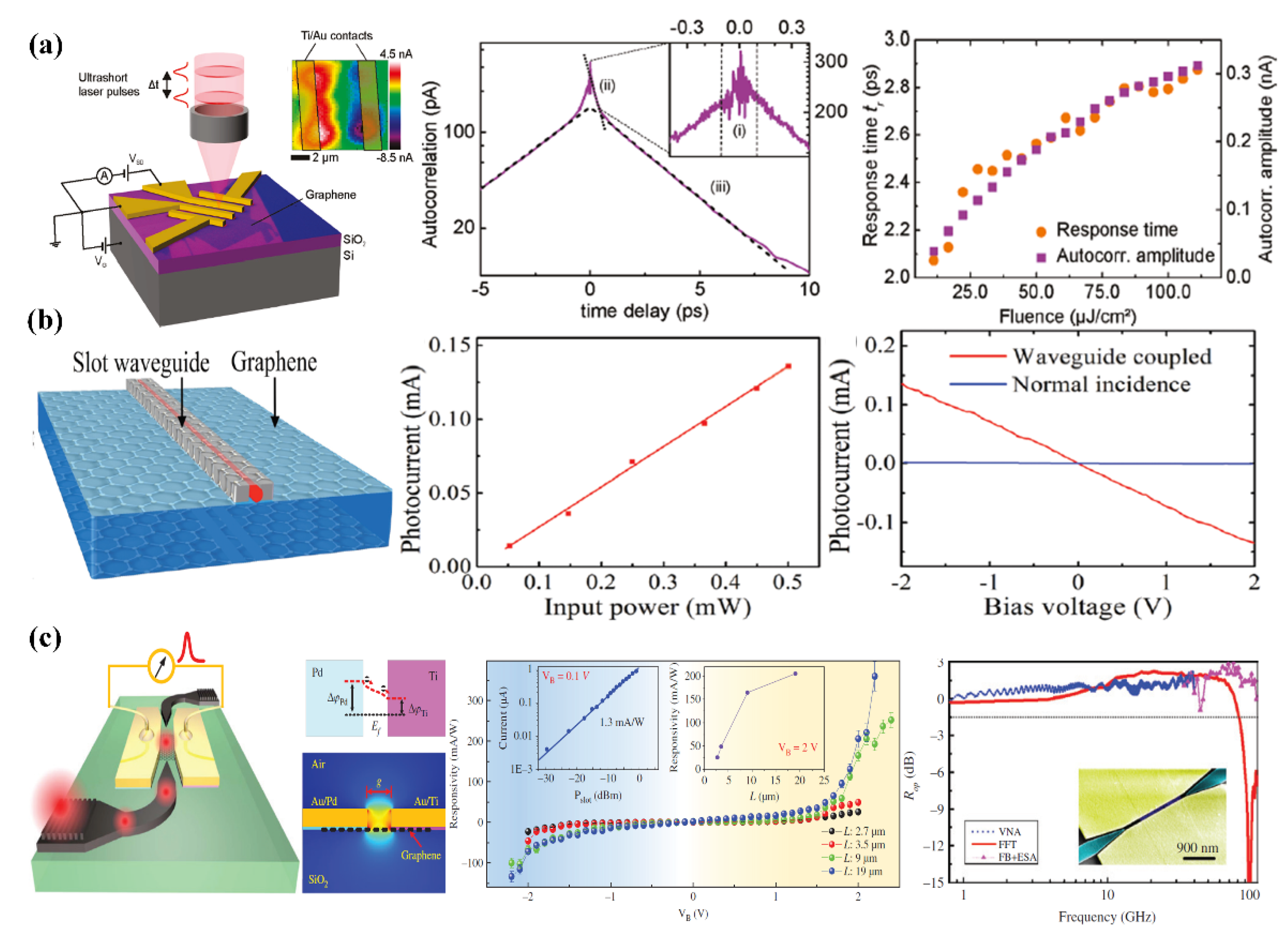
Absorption Material | Responsivity | Bandwidth | Size | Operation Wavelength Range | ||||||||||
|---|---|---|---|---|---|---|---|---|---|---|---|---|---|---|
InGaAs [68] | [41] |
0.68 A/W | 32 GHz | 1 μm | 1260 nm~1360 nm | |||||||||
InP [69] | [42] |
0.8 A/W | 40 GHz | 5 μm | 1240 nm~1650 nm | |||||||||
InP [70] | [43] |
0.5 A/W | 130 GHz | N. A. | 1310 nm and 1550 nm | |||||||||
α-Ge [71] | [44] |
0.35 A/W | >100 GHz | 20 μm | 1270 nm~1330 nm | |||||||||
Ge [55] | [26] |
0.3 A/W | 265 GHz | 10 μm | 1550 nm | |||||||||
Graphene [57] | [29] |
0.36 A/W | >110 GHz | 20 μm | 1540 nm | |||||||||
Graphene [59] | [32] |
0.6 A/W | 78 GHz | 30 μm | 1550 nm | |||||||||
Graphene [62] | [35] |
0.5 A/W | >110 GHz | 6 μm | 1480 nm~1620 nm | |||||||||
Graphene [63] | [36] |
0.4 A/W | >40 GHz | 20 μm | 1550 nm and 2000 nm |
References
- Xu, M.; David, J.M.; Kim, S.H. The fourth industrial revolution: Opportunities and challenges. Int. J. Financ. Res. 2018, 9, 90–95.
- Ashton, K. That ‘Internet of Things’ thing. RFID J. 2009, 22, 97–114.
- Wang, L.; Von Laszewski, G.; Younge, A.; He, X.; Kunze, M.; Tao, J.; Fu, C. Cloud computing: A perspective study. New Gener. Comput. 2010, 28, 137–146.
- Tsai, C.-W.; Lai, C.-F.; Chao, H.-C.; Vasilakos, A.V. Big data analytics: A survey. J. Big Data 2015, 2, 21.
- Miller, S. Optical Fiber Telecommunications; Elsevier: Amsterdam, The Netherlands, 2012.
- Jalali, B.; Fathpour, S. Silicon photonics. J. Lightwave Technol. 2006, 24, 4600–4615.
- Soref, R. The past, present, and future of silicon photonics. IEEE J. Sel. Top. Quantum Electron. 2006, 12, 1678–1687.
- Thomson, D.; Zilkie, A.; Bowers, J.E.; Komljenovic, T.; Reed, G.T.; Vivien, L.; Marris-Morini, D.; Cassan, E.; Virot, L.; Fédéli, J.-M. Roadmap on silicon photonics. J. Opt. 2016, 18, 073003.
- Novoselov, K.S.; Geim, A.K.; Morozov, S.V.; Jiang, D.; Katsnelson, M.I.; Grigorieva, I.V.; Dubonos, S.V.; Firsov, A.A. Two-dimensional gas of massless Dirac fermions in graphene. Nature 2005, 438, 197–200.
- Ponomarenko, L.A.; Yang, R.; Mohiuddin, T.M.; Katsnelson, M.I.; Novoselov, K.S.; Morozov, S.V.; Zhukov, A.A.; Schedin, F.; Hill, E.W.; Geim, A.K. Effect of a high-κ environment on charge carrier mobility in graphene. Phys. Rev. Lett. 2009, 102, 206603.
- Gan, X.; Shiue, R.-J.; Gao, Y.; Meric, I.; Heinz, T.F.; Shepard, K.; Hone, J.; Assefa, S.; Englund, D. Chip-integrated ultrafast graphene photodetector with high responsivity. Nat. Photonics 2013, 7, 883–887.
- Phare, C.T.; Daniel Lee, Y.-H.; Cardenas, J.; Lipson, M. Graphene electro-optic modulator with 30 GHz bandwidth. Nat. Photonics 2015, 9, 511–514.
- Agarwal, H.; Terrés, B.; Orsini, L.; Montanaro, A.; Sorianello, V.; Pantouvaki, M.; Watanabe, K.; Taniguchi, T.; van Thourhout, D.; Romagnoli, M.; et al. 2D-3D integration of hexagonal boron nitride and a high-κ dielectric for ultrafast graphene-based electro-absorption modulators. Nat. Commun. 2021, 12, 1070.
- Yu, L.; Dai, D.; He, S. Graphene-based transparent flexible heat conductor for thermally tuning nanophotonic integrated devices. Appl. Phys. Lett. 2014, 105, 251104.
- Gan, S.; Cheng, C.; Zhan, Y.; Huang, B.; Gan, X.; Li, S.; Lin, S.; Li, X.; Zhao, J.; Chen, H.; et al. A highly efficient thermo-optic microring modulator assisted by graphene. Nanoscale 2015, 7, 20249–20255.
- Schall, D.; Mohsin, M.; Sagade, A.A.; Otto, M.; Chmielak, B.; Suckow, S.; Giesecke, A.L.; Neumaier, D.; Kurz, H. Infrared transparent graphene heater for silicon photonic integrated circuits. Opt. Express 2016, 24, 7871–7878.
- Yu, L.; Yin, Y.; Shi, Y.; Dai, D.; He, S. Thermally tunable silicon photonic microdisk resonator with transparent graphene nanoheaters. Optica 2016, 3, 159–166.
- Xu, Z.; Qiu, C.; Yang, Y.; Zhu, Q.; Jiang, X.; Zhang, Y.; Gao, W.; Su, Y. Ultra-compact tunable silicon nanobeam cavity with an energy-efficient graphene micro-heater. Opt. Express 2017, 25, 19479–19486.
- Suk, J.W.; Kitt, A.; Magnuson, C.W.; Hao, Y.; Ahmed, S.; An, J.; Swan, A.K.; Goldberg, B.B.; Ruoff, R.S. Transfer of CVD-Grown Monolayer Graphene onto Arbitrary Substrates. ACS Nano 2011, 5, 6916–6924.
- Matsuda, Y.; Deng, W.-Q.; Goddard, W.A. Contact Resistance for “End-Contacted” Metal−Graphene and Metal−Nanotube Interfaces from Quantum Mechanics. J. Phys. Chem. C 2010, 114, 17845–17850.
- Reed, G.T.; Mashanovich, G.; Gardes, F.Y.; Thomson, D.J. Silicon optical modulators. Nat. Photonics 2010, 4, 518–526.
- Almeida, V.R.; Barrios, C.A.; Panepucci, R.R.; Lipson, M. All-optical control of light on a silicon chip. Nature 2004, 431, 1081–1084.
- Xu, Q.; Schmidt, B.; Pradhan, S.; Lipson, M. Micrometre-scale silicon electro-optic modulator. Nature 2005, 435, 325–327.
- Benedikovic, D.; Virot, L.; Aubin, G.; Amar, F.; Szelag, B.; Karakus, B.; Hartmann, J.-M.; Alonso-Ramos, C.; Roux, X.L.; Crozat, P.; et al. 25 Gbps low-voltage hetero-structured silicon-germanium waveguide pin photodetectors for monolithic on-chip nanophotonic architectures. Photonics Res. 2019, 7, 437–444.
- Benedikovic, D.; Virot, L.; Aubin, G.; Hartmann, J.-M.; Amar, F.; Le Roux, X.; Alonso-Ramos, C.; Cassan, E.; Marris-Morini, D.; Crozat, P.; et al. 40 Gbps heterostructure germanium avalanche photo receiver on a silicon chip. Optica 2020, 7, 775–783.
- Lischke, S.; Peczek, A.; Morgan, J.S.; Sun, K.; Steckler, D.; Yamamoto, Y.; Korndörfer, F.; Mai, C.; Marschmeyer, S.; Fraschke, M.; et al. Ultra-fast germanium photodiode with 3-dB bandwidth of 265 GHz. Nat. Photonics 2021, 15, 925–931.
- Wang, J.; Cheng, Z.; Chen, Z.; Wan, X.; Zhu, B.; Tsang, H.K.; Shu, C.; Xu, J. High-responsivity graphene-on-silicon slot waveguide photodetectors. Nanoscale 2016, 8, 13206–13211.
- Luan, C.; Liu, Y.; Ding, Y.; Hu, H. 2-um high-speed graphene electro-optic modulator based on silicon slot microring resonator. In Proceedings of the Conference on Lasers and Electro-Optics, Washington, DC, USA, 10–15 May 2020; p. JTh2F.34.
- Ding, Y.; Cheng, Z.; Zhu, X.; Yvind, K.; Dong, J.; Galili, M.; Hu, H.; Mortensen, N.A.; Xiao, S.; Oxenløwe, L.K. Ultra-compact integrated graphene plasmonic photodetector with bandwidth above 110 GHz. Nanophotonics 2020, 9, 317–325.
- Shu, H.; Su, Z.; Huang, L.; Wu, Z.; Wang, X.; Zhang, Z.; Zhou, Z. Significantly High Modulation Efficiency of Compact Graphene Modulator Based on Silicon Waveguide. Sci. Rep. 2018, 8, 991.
- Wang, Y.; Li, X.; Jiang, Z.; Tong, L.; Deng, W.; Gao, X.; Huang, X.; Zhou, H.; Yu, Y.; Ye, L.; et al. Ultrahigh-speed graphene-based optical coherent receiver. Nat. Commun. 2021, 12, 5076.
- Yan, S.; Zuo, Y.; Xiao, S.; Oxenløwe, L.K.; Ding, Y. High-performance Silicon/Graphene Photodetector Employing Double Slot Structure. In Proceedings of the Conference on Lasers and Electro-Optics, San Jose, CA, USA, 9–14 May 2021; p. STh5B.2.
- Schall, D.; Neumaier, D.; Mohsin, M.; Chmielak, B.; Bolten, J.; Porschatis, C.; Prinzen, A.; Matheisen, C.; Kuebart, W.; Junginger, B.; et al. 50 GBit/s Photodetectors Based on Wafer-Scale Graphene for Integrated Silicon Photonic Communication Systems. ACS Photonics 2014, 1, 781–784.
- Ma, Z.; Kikunaga, K.; Wang, H.; Sun, S.; Amin, R.; Maiti, R.; Tahersima, M.H.; Dalir, H.; Miscuglio, M.; Sorger, V.J. Compact Graphene Plasmonic Slot Photodetector on Silicon-on-Insulator with High Responsivity. ACS Photonics 2020, 7, 932–940.
- Ma, P.; Salamin, Y.; Baeuerle, B.; Josten, A.; Heni, W.; Emboras, A.; Leuthold, J. Plasmonically Enhanced Graphene Photodetector Featuring 100 Gbit/s Data Reception, High Responsivity, and Compact Size. ACS Photonics 2019, 6, 154–161.
- Guo, J.; Li, J.; Liu, C.; Yin, Y.; Wang, W.; Ni, Z.; Fu, Z.; Yu, H.; Xu, Y.; Shi, Y.; et al. High-performance silicon−graphene hybrid plasmonic waveguide photodetectors beyond 1.55 μm. Light Sci. Appl. 2020, 9, 29.
- Shiue, R.-J.; Gao, Y.; Wang, Y.; Peng, C.; Robertson, A.D.; Efetov, D.K.; Assefa, S.; Koppens, F.H.L.; Hone, J.; Englund, D. High-Responsivity Graphene–Boron Nitride Photodetector and Autocorrelator in a Silicon Photonic Integrated Circuit. Nano Lett. 2015, 15, 7288–7293.
- Schuler, S.; Schall, D.; Neumaier, D.; Schwarz, B.; Watanabe, K.; Taniguchi, T.; Mueller, T. Graphene Photodetector Integrated on a Photonic Crystal Defect Waveguide. ACS Photonics 2018, 5, 4758–4763.
- Schuler, S.; Muench, J.E.; Ruocco, A.; Balci, O.; van Thourhout, D.; Sorianello, V.; Romagnoli, M.; Watanabe, K.; Taniguchi, T.; Goykhman, I.; et al. High-responsivity graphene photodetectors integrated on silicon microring resonators. Nat. Commun. 2021, 12, 3733.
- Mišeikis, V.; Marconi, S.; Giambra, M.A.; Montanaro, A.; Martini, L.; Fabbri, F.; Pezzini, S.; Piccinini, G.; Forti, S.; Terrés, B.; et al. Ultrafast, Zero-Bias, Graphene Photodetectors with Polymeric Gate Dielectric on Passive Photonic Waveguides. ACS Nano 2020, 14, 11190–11204.
- Mauthe, S.; Baumgartner, Y.; Sousa, M.; Ding, Q.; Rossell, M.D.; Schenk, A.; Czornomaz, L.; Moselund, K.E. High-speed III-V nanowire photodetector monolithically integrated on Si. Nat. Commun. 2020, 11, 4565.
- Xue, Y.; Han, Y.; Tong, Y.; Yan, Z.; Wang, Y.; Zhang, Z.; Tsang, H.K.; Lau, K.M. High-performance III-V photodetectors on a monolithic InP/SOI platform. Optica 2021, 8, 1204–1209.
- Runge, P.; Zhou, G.; Ganzer, F.; Mutschall, S.; Seeger, A. Waveguide integrated InP-based photodetector for 100Gbaud applications operating at wavelengths of 1310nm and 1550nm. In Proceedings of the 2015 European Conference on Optical Communication (ECOC), Valencia, Spain, 27 September–1 October 2015; pp. 1–3.
- Salamin, Y.; Ma, P.; Baeuerle, B.; Emboras, A.; Fedoryshyn, Y.; Heni, W.; Cheng, B.; Josten, A.; Leuthold, J. 100 GHz Plasmonic Photodetector. ACS Photonics 2018, 5, 3291–3297.