Strain sensors, otherwise known as strain gauges, are fueled by various nanomaterials, among which graphene has attracted great interest in recent years, due to its unique electro-mechanical characteristics. Graphene shows not only exceptional physical properties but also has remarkable mechanical properties, such as piezoresistivity, which makes it a perfect candidate for strain sensing applications.
1. Introduction
With the advent of the internet-of-things (IoT), smart, ubiquitous, pervasive sensing is rapidly gaining importance for providing reliable information at unprecedented sensitivity to enable new applications in consumer electronics
[1][2][3][1,2,3], healthcare
[4][5][6][4,5,6], manufacturing and structural monitoring
[7][8][7,8], transportation
[9][10][9,10], defense and surveillance
[11][12][13][11,12,13]; as well as to fuel research in fundamental, applied and translational science
[14]. Among the various physical measurands, the monitoring of strain finds use in numerous applications and industrial products where the fundamental detection principle relies on the change in electrical properties of the strain sensing element as a result of applied pressure or force. Strain sensors essentially rely on four fundamental sensing modalities which are capacitive, piezoelectric, piezoresistive and optical sensing
[15]. Among these, piezoresistive sensors, with their low-cost-fabrication and easy data analysis advantages, have gathered significant attention.
Typically, sensors based on piezoresistivity rely on transducing external mechanical loading into resistance change, which usually follows a linear relationship
[16]. Commonly, piezoresistive sensors harness the piezoresistive effect of the sensing material whereby its conductance changes with applied strain, along with change in resistance of the entire sensor assembly due to geometry change upon deformation. To design high-performance piezoresistive sensors, different parameters such as stretchability, sensitivity, dynamic range, limit of detection, accuracy, response speed, stability, durability, fabrication cost and simplicity should be considered. Out of these design criteria, the fundamental figure-of-merit for a strain sensor is its sensitivity, which is evaluated by the gauge factor (GF), formally defined as the ratio of relative resistance change in the sensing element to the mechanical strain acting on it (GF = ΔR/R/ε).
To date, various materials have been investigated for use as strain sensing elements, in an effort to optimize the response of the strain sensor with respect to the attributes mentioned above. Realizing a strain sensor operating at a wide strain range with good sensitivity has been an especially huge challenge. To overcome the problem of low sensitivity, different approaches have been proposed including doping, defect deformation and exploiting different piezoresistive sensing mechanisms along with sensing materials
[17][18][19][20][21][17,18,19,20,21].
Among the most typical strain sensing materials are metals. However, strain sensors based on metals, otherwise known as metal-foil gauges, primarily rely on resistance change due to dimensional change of electrically conducting thin lines typically structured in the form of a serpentine, and as such the gauge factors are typically limited to single digits
[14][22][14,22]. Several other strain sensors with different types of semiconductor piezoresistive materials, including doped polysilicon have also been developed, which offer much higher gauge factors compared to metal-foil counterparts
[23].
As an alternative to some of these conventional materials like metals, metal oxides, semiconductors and ceramics which suffer either from intrinsic hardness, brittleness, low strain range or poor scalability, in recent years, carbon-based materials have been on the forefront of “sensor research”, including strain sensing
[21][22][23][24][25][21,22,23,24,25]. As such, nanomaterials including carbon nanotubes (CNT) and graphene have both been reported as functional materials to realize strain sensors
[24]. While CNTs have an almost one-dimensional (1D) structure
[25], graphene has an ideal two-dimensional (2D) structure which potentially allows conventional device fabrication by planar, semiconductor process technologies. Additionally, its piezoresistive property
[26][27][26,27] together with its exceptional physical, electrical
[28] and mechanical properties (Young’s modulus on the order of 1 TPa)
[29] render graphene an ideal candidate for strain sensors
[30].
2. Fundamental Material Properties and Piezoresistive Effect in Graphene
Graphene is a crystalline allotrope of carbon, which consists of a single-layer sheet of sp
2 hybridized carbon atoms. After its exploration in 2004, graphene it has drawn a lot of attention due to its excellent electrical, mechanical, optical and magnetic properties
[31][32][33][34][35][36][42,43,44,45,46,47].
2.1. Electrical Properties
Studies on the electronic properties of graphene show that it is a new class of material resembling a zero-bandgap semiconductor and even acting more like a metal, yet still harboring the potential to have a bandgap and Fermi level by various methods, including doping
[37][48]. Electronic properties of graphene also strongly depend on crystallite thickness. In single layer graphene, the band gap is zero, making it behave like a semiconductor or semi-metal, while the multilayer graphene shows metallic behavior as a result of the overlap in carrier wave function, which is due to the multiple graphene layers stacking
[38][49]. The unique band structure of monolayer graphene leads to excellent traits, such as ballistic transport properties and anomalous quantum Hall effects, ultrahigh mobility (200,000 cm
2/V·s) and high specific electrical conductivity (SEC) (0.95–1.67 S m
2/g)
[39][50], which can vary with applied strain.
Earlier study has shown the effect of the applied strain on opening the band gap of single-crystal graphene at the Fermi level, which results in the decrease of its electrical conductivity
[40][51]. At low energies, graphene contains two linear energy bands that meet at high symmetric points and are isotropic with regard to the points at equilibrium. Effect of different strain types on the electronic properties of graphene reveals that, when isotropic strain is applied, graphene shows electronic properties that are independent of the isotropic strain since the isotropic strain follows crystal symmetries
[41][52]. Strain can be intentionally or naturally imposed on graphene. By bending the substrates on which graphene is extended without slippage, uniaxial strain can be generated. To understand the effect of the uniaxial strain, armchair and zigzag graphene nanoribbons were studied, and they were reported to have different electronic properties. The electronic properties of the zigzag nanoribbons were independent of the uniaxial strain whereas the armchair nanoribbons were predicted to have energy gaps varying with the armchair shape
[42][53].
2.2. Mechanical Properties
Graphene, as a two-dimensional one atomic layer thick material, sustains up to 25% in-plane tensile strain, making it one of the most flexible, uniform, zero band-gap semiconductors
[43][54]. Graphene is known for its very high in-plane stiffness (high Young’s modulus), and the highest ever measured mechanical strength
[33][44][45][44,55,56]. The 2D breaking strength and elastic stiffness of free-standing monolayer graphene membranes measured by an atomic force microscope (AFM) showed 42 N·m
−1 and 340 N·m
−1, respectively
[33][44]; rendering graphene as the strongest material ever measured. These correspond to near theoretical limits including a mechanical stiffness of 1 TPa and an intrinsic tensile strength of 130 GPa at 25% strain, which are also comparable to in-plane values of graphite and single-walled and multi-walled carbon nanotubes
[33][44]. It is important to note, however, that such mechanical properties largely depend on the testing temperature, sample geometry and even the measurement technique utilized. For instance, a layer of suspended exfoliated graphene located on a trench pattern of silicon oxide/silicon substrate was analyzed with AFM, showing graphene thickness of less than 10 nm, spring constant in the range of 1 to 5 N/m, and Young’s modulus of 0.5 TPa, which is less than that of bulk graphite typically ranging around 1 TPa
[46][57]. Overall, the remarkable mechanical properties of graphene are very important, especially for flexible, stretchable electronics and/or wearable applications where robust and functional materials with excellent electronic and structural properties are needed
[47][58].
2.3. Piezoresistivity
A piezoresistive effect is observed when a change in electrical resistivity of a material occurs as a result of applied stress. In other words, piezoresistivity is the change in resistivity of a material as a function of deformation. Germanium
[48][59], silicon
[49][60] and polycrystalline silicon
[50][61] are the most common semiconductor materials that show a piezoresistive effect, and they are frequently used in MEMS for measurement of strain, pressure, acceleration, flow and tactile sensing, as well as haptics applications.
Graphene has attracted a lot of attention, not only due to being the thinnest known material and having unique electrical and mechanical properties, but also due to having a linear change of resistance versus strain, making it a good candidate for piezoresistive sensor applications
[51][62]. In this regard, piezoresistivity of multilayer graphene on poly (methyl methacrylate) (PMMA) substrate was investigated through a bending test that showing high piezoresistivity with a gauge factor of 50, demonstrating the potential of graphene for strain sensing applications
[52][63]. In addition, Anderson D. Smith et al. verified the piezoresistive effect in graphene by applying uniaxial and biaxial strains
[53][64]. Gauge factors of biaxial strained devices were found to be higher than that of uniaxial ones.
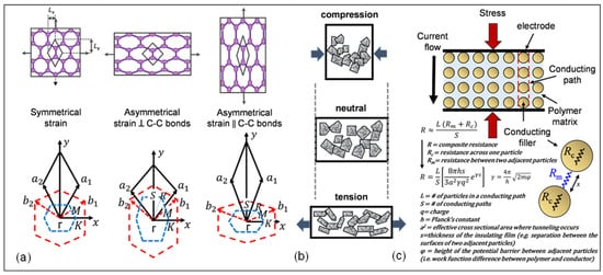
The piezoresistivite effect in graphene has been elucidated with three different mechanisms which include: (a) structure deformation, (b) over-connection of graphene sheets, and (c) the tunneling effect among neighboring sheets.
- (a) Structure Deformation
Electrical-mechanical coupling in graphene can be observed when significant elongation in graphene causes changes in its electrical properties and band structure. Recent studies on strained graphene demonstrate that changes in electrical properties of graphene are related to the type of strain distribution. In symmetrical strain distribution, additional scattering and resistance decrease is observed while no change occurs in other graphene properties such as band-gap opening
[54][55][56][57][58][59][65,66,67,68,69,70]. On the other hand, asymmetrical strain distribution in graphene results in opening of band gaps at the Fermi level, which is explained by pseudo-magnetic field. Strain distributions in graphene significantly modify the band structure of graphene around the Fermi level, resulting in remarkable change of the pseudogap width in the case of symmetrical strain distributions and band-gap opening in the case of asymmetrical strain distributions. The band gap is enlarged by increasing the amount of strain, reaching a maximum value of 0.486 eV at 12.2% strain parallel to C-C bonding, and to a maximum of 0.170 eV at 7.3% strain perpendicular to C-C bonding (
Figure 1a)
[40][51].
Figure 1. Piezoresistivity mechanisms of graphene: (
a) symmetrical strain distribution, asymmetrical strain distribution perpendicular to C-C bonds and asymmetrical strain distribution parallel to C-C bonds
[40][51]; (
b) schematic illustration of piezoresistivity of graphene sheets
[60][71]; (
c) schematic illustration of the tunneling model.
Reprinted with permission from ref. [72]. Copyright Clearance Center.
- (b) Over-connected Graphene Sheets
As shown in
Figure 1b, a larger sheet of graphene can be thought of as a conductive network of smaller connected sheets or flakes. From a nanoscopic perspective, the distortion of a small graphene sheet alters the resistivity of the single sheet, which can consecutively trigger a resistance change in the entire conducting system. Thus, the stress response of the graphene network relies primarily on the contact strength of the neighboring plates from a macroscopic point-of-view. Overlap area and contact resistance determine the conductivity between the neighboring flakes. As displayed in
Figure 1b, the overlap between neighboring flakes becomes smaller or greater such that the resistance changes upon tensile or compressive loading making graphene a suitable material for strain sensing applications
[30][60][30,71].
- (c) Tunneling Effect among Neighboring Graphene Sheets
It is known that the distance between two graphene sheets specify the conductivity of graphene. Due to the tunneling effect, current can flow from one single graphene sheet to another. As a result, the resistance increases exponentially and proportionally with the distance (
Figure 1c)
[61][72]. This mechanism can be used to achieve higher GF in graphene-based strain sensors. As shown in
Figure 1c, by assuming that the resistance of the matrix is constant everywhere, the resistance of the paths perpendicular to the current flow can be ignored, and thus the number of conducting particles between electrodes, as well as the number of conducting paths, becomes a factor in this relationship. The total resistance can then be calculated as R, which is shown in
Figure 1c.
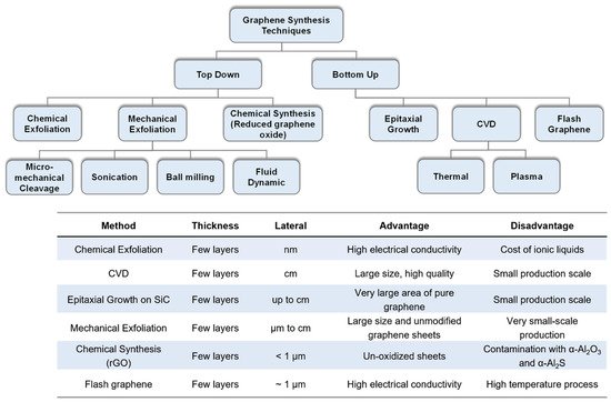
3. Methods of Obtaining and Transferring Graphene
Despite its superior electrical and mechanical properties, the challenges in obtaining pristine graphene limit the widespread use of this 2D material in device applications. In an effort to address this problem, numerous techniques were investigated to obtain thin graphitic films and few layer graphene (FLG). Initial demonstrations primarily through mechanical exfoliation followed by transfer of graphene onto silicon substrates, marked a major breakthrough in graphene research
[62][73]. Even though mechanical exfoliation (i.e., Scotch tape method) provides the highest quality graphene, this approach has some disadvantages such as depending largely on the hand skills of the researcher, lack of repeatability and scalability, as well as limitations on graphene flake size and shape being small and irregular.
Therefore, research on obtaining high-quality graphene along with its integration to different substrates which often requires transfer methods, has received serious effort especially over the past two decades. The method with which graphene is obtained directly affects the quality of graphene including its electrical, mechanical and piezoresistive properties. Different methods which are classified as bottom-up and top-down processes have been utilized in order to obtain high-quality graphene. The most commonly used methods are: chemical exfoliation
[63][74], chemical vapor deposition (CVD)
[64][75], epitaxial growth
[65][76], mechanical and reduction of graphene oxide rGO
[66][67][77,78], and flash graphene synthesis
[68][79]. Graphical overview of these techniques along with the major advantages and drawbacks of each approach are summarized in
Figure 2.
Figure 2. Overview of the most common techniques to obtain graphene categorized based on top-down and bottom-up processes, along with a tabular comparison on the thickness, lateral size, fundamental advantages and disadvantages of each technique.
Reprinted with permission from ref. [74].
4. Graphene-Based Strain Sensors
There are a number of studies in which graphene is used as a strain sensing material. Typically used to fabricate flexible graphene-based strain sensors, graphene can be compounded with elastomers to realize flexible strain sensors with sufficient piezoresistive performance, owing to the excellent electro-mechanical properties of graphene, along with the stretchability and flexibility of polymer matrix. A number of polymers have been utilized in strain sensor applications, where flexibility and stretchability factors are concerned in order to obtain high sensitivity with robust mechanical strength. In this regard, PDMS, PET, 3M elastic adhesive tape, PU and natural rubber have been employed to fabricate graphene-based strain sensors
[69][139].
The performance, more specifically the gauge factor, of these polymer integrated graphene-based strain sensors varies due to different forms of graphene
(as detailed in Section 3) and their implementation methods in polymeric/elastomer matrix structures. We therefore classify graphene strain gauges based on the three most common methods with which graphene is obtained namely: (a) CVD, (b) exfoliation, and (c) reduction of GO. Tabular summary of existing strain gauges based on the three different forms of graphene is provided in
Table 1, along with their gauge factor and strain range as performance metrics.
Table 1. Classification of graphene-based strain gauges in terms of the method used to obtain graphene, along with the device topology and performance metrics like gauge factor and strain range.
|
Graphene Synthesis Method
|
Device Topology
|
Gauge
Factor
|
Strain
Range
|
Ref.
|
|
CVD
|
RPECVD graphene on mica substrate
|
325
|
0.30%
|
[70][140]
|
|
Graphene-nano graphene sheets on finger
|
500
|
1%
|
[71][136]
|
|
Suspended CVD graphene membrane
|
1.6
|
0.25%
|
[23]
|
|
Suspended CVD graphene membrane
|
3.67
|
0.29%
|
[72][141]
|
|
CVD graphene on suspended perforated SiNx membrane
|
4.4
|
0.22%
|
[73][142]
|
|
Graphene glow sensor
|
2.4
|
1.8%
|
[74][143]
|
|
CVD graphene woven fabric on PDMS
|
106
|
10%
|
[75][144]
|
|
Graphene-graphene woven on PDMS
|
223
|
3%
|
[76][145]
|
|
Fragmented graphene foam on PDMS
|
15–29
|
77%
|
[77][146]
|
|
Graphene tactile sensor
|
1.4
|
-
|
[78][147]
|
|
CVD graphene on PDMS
|
6.1
|
1%
|
[79][148]
|
|
braided graphene belts sensor
|
175.16
|
55%
|
[80][149]
|
|
planar and crumpled graphene
|
20.1
|
105%
|
[81][150]
|
|
graphene/g-C3N4 heterostructure on PDMS
|
1.89
|
25%
|
[82][151]
|
|
Graphene-single layer graphene on finger
|
42.2
|
20%
|
[26]
|
|
Graphene wrapped CNTs
|
20
|
1.20%
|
[83][152]
|
|
PDMS graphene reinforced CNT network
|
0.36
|
-
|
[84][153]
|
|
Exfoliated graphene
|
Spray-deposited graphene on a flexible plastic substrate
|
10–100
|
1.70%
|
[85][154]
|
|
Mechanical exfoliated graphene on a silicon wafer
|
10–15
|
0.08%
|
[86][155]
|
|
Mechanical exfoliated graphene nanoribbons
|
0.6
|
0.054%
|
[87][156]
|
|
Mechanical exfoliated graphene nanoribbons
|
8.8
|
5%
|
[88][157]
|
|
Graphene-printed fragments
|
125
|
0.30%
|
[89][158]
|
|
Mechanical exfoliated graphene nanoribbons
|
1.9
|
3%
|
[90][159]
|
|
Graphene solution coated on polypropylene film
|
1000
|
0.05–0.265%
|
[91][160]
|
|
Polymer-functionalized hydrogen-exfoliated graphene
|
10
|
0.35%
|
[92][161]
|
|
Graphene nanoplatelet on PDMS
|
62.5
|
2.5–25%
|
[93][162]
|
|
PDMS-graphene nanoplatelet/CNT hybrids
|
1000
|
18%
|
[94][163]
|
|
Carbon nanotube-graphene nanoplatelet hybrid film
|
<1
|
-
|
[95][164]
|
|
rGO
|
Mechanical exfoliated Graphene ripple on PDMS
|
−2
|
20%
|
[96][165]
|
|
3D graphene foam-PDMS nanocomposite
|
178
|
30%
|
[97][166]
|
|
rGO on a PET substrate
|
61.5
|
0.01–0.04%
|
[98][167]
|
|
rGO membrane porous structure
|
15.2–46.1
|
1%
|
[99][168]
|
|
PDMS-cellulose-rGO/CNFs hybrids
|
9.4
|
70%
|
[100][169]
|
|
3D porous PDMS CNT/rGO hybrid
|
1.6
|
80%
|
[101][170]
|
|
Polyurethane-silver nanowires/graphene hybrids
|
20–400
|
0.3–1%
|
[102][171]
|
|
rGO-microtube on PDMS
|
630
|
50%
|
[103][172]
|
|
Crumpled graphene-nanocellulose composite on elastomer matrix
|
−7.1
|
100%
|
[104][173]
|
|
rGO doped with polystyrene nanoparticles (PS) on PDMS
|
250
|
1.05%
|
[105][174]
|
|
Polymerized rGO on TPU
|
23.15–6583
|
550%
|
[106][175]
|
|
rGO mesh on an LCP substrate
|
375–473
|
0.1–1.4%
|
[107][176]
|
|
rGO-fish scale like on an elastic tape
|
16
|
82%
|
[108][177]
|
|
rGO-conductive cotton fabric
|
-
|
0.02–0.35%
|
[109][178]
|
|
rGO-FET on polyethersulfone (PES)
|
20
|
50%
|
[110][179]
|
5. Applications of Graphene-Based Strain Sensor
5.1. Wearable Devices
One major area where strain sensors are used vastly as different applications is wearable electronics. For healthcare applications, wearable sensors have been attached to gloves, organs, and skins to observe physiological activities of the body such as monitoring heart rate, wrist pulse, motion, blood pressure, intraocular pressure, vibration of vocal cords, movement of joints and other health-related situations
[54][55][56][111][112][113][114][115][116][65,66,67,180,181,182,183,184,185]. Since the mechanical properties of piezoresistive materials such as flexibility and stretchability are vital in wearable sensors, only a limited selection of materials meet the requirements to be used in these sensors. Therefore, graphene has attained promising interest compared to other materials
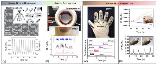
[117][118][119][186,187,188]. Inspired by this fact, a graphene woven fabric (GWF) on PDMS and a medical tape composite has been reported as a wearable strain sensor for detecting body motion (
Figure 3a)
[118][187]. The sensor offers different gauge factor values of 35, 103 and 106, at strains of 0.2%, 2–6% and >7%, respectively.
Figure 3. (
a) Optical microscope image of graphene woven fabrics (GWFs)-PDMS-tape composite film (scale bar 0.1 mm) and the relative resistance change as a function of applied strain varying between 0% and 0.2%.
Reprinted with permission from ref. [187]. Copyright (
2014) John Wiley and Sons. (b) Photograph of a strain sensor attached to the vibrating membrane of a loudspeaker and to a participants’ throat, where similar change in relative resistance was observed as the same sentence was played from the loudspeaker (black curve) and read out loud (red curve).
Reprinted with permission from ref. [189]. Copyright (
2015) Springer Nature. (c) Application of graphene nanopaper-based sensors on a glove is imaged and the transitions between the corresponding resistance changes of the strain sensor by the motion of each of the fingers.
Reprinted with permission from ref. [173]. Copyright (2013) John Wiley and Sons. (
d) Observation of relative resistance changes in the strain sensor on a glove when the finger bends or unbends and using a rosette gauge on the glove to detect the direction of principal strain by applying stretch gently.
Reprinted with permission from ref. [143]. Copyright (2013) Elsevier.
In another study, a device for detecting and identifying sound-signals with the help of strain sensing mechanism of the graphene woven fabric (GWF)-based sensor on PDMS was investigated
[120][189]. The sensor was utilized in the form of a patch that was attached to human throat to investigate resistance changes due to the movement and vibration of throat muscles during vocalization. To benchmark the sensor response, the same sentence was played by a loudspeaker and read out loud by a person who had the sensor attached to his throat, where similar resistance change was observed in both testing conditions. The sensor showed high sensitivity (even to the low frequencies), and reliability.
Figure 3c demonstrates graphene nanopaper-based strain sensors attached onto a feather glove as a possible real-life application of wearable sensors in order to detect the movements of the fingers. The response behavior of sensors located on the fingers were tested by bending and stretching all five fingers at a frequency of 1 Hz. Also, high strain in range of 0–100% was measured in this experiment. The gauge factors for stretchable nanopaper increased from 1.6 at 10% strain to 7.1 at 100% strain. Besides, the solution process-based fabrication method made the strain gauge superior in terms of cost and mass production ability
[104][173]. To make high-strain sensors, this technique uses crumpled graphene and nanocellulose. Free-standing flexible nanopapers were created by vacuum filtering, and their 3D structure allowed them to be successfully embedded in an elastomer matrix to produce stretchy nanopapers. However, there is still a restriction about measuring high strains over 50% that are caused by stretching and contracting motions in human joints. So, using nanopapers may be a solution to detect strain over 100%. This application shows a gauge factor of 7.1 at 100% of strain which is ~10 times higher than those of 1D materials such as CNTs and AgNWs in a similar device arrangement.
A single strain gauge is typically capable of measuring the strain that has the same direction with the position of the gauge
[111][180]. That is why the aligning a strain sensor within the direction of the strain is necessary to obtain an immediate response to the deformation. Since recognizing the principal strain directions on human skin is generally impractical, it is not easy to measure the predominant strain directly.
Figure 3d illustrates an application onto a glove as a sensor to detect the direction and magnitude of the predominant strains. Changes occurred in a normalized resistance value when the rosette gauge was stretched. When the finger bends, the strain caused by the finger is taken up by the first glove layer and then transmitted to the rosette gauge. The rosette gauge responds quickly to the bending of the finger, and its signal amplitude is proportional to the amount of strain caused by the bending: the more the finger bends, the more the signal amplitude grows. The strain caused by bending the finger is estimated to be 1.3%, 1.2%, 1.4%, and 1.6%, respectively, based on the resistance change. The strain sensor also was recovered perfectly after straightening the finger. Both the magnitude of the applied force and the direction of the major strains on the skin were detected simultaneously by setting the strain gauges in the rosette arrangement. The green, red and blue lines in the resistance plot in
Figure 3d correspond to 3-gauge sensor a, b and c. The ”a” gauge and the other two gauges, ”b” and ”c”, are positioned at the same distance and are oriented at the same angle with respect to the “a” gauge
[74][143].
Along with wearability, applications deeming stretchability and flexibility are yet another area where the use of graphene as a strain sensing element offers advantages. For instance, a highly sensitive graphene embedded viscoelastic polymer nanocomposite was reported as a flexible strain sensor, which could measure very small pressures of pulse, blood pressure and even the minute mechanical loading due to walking of small insects. In this work, the mobility of graphene fillers was enhanced by a lightly cross-linked polymer matrix providing high viscosity. The resulting nanocomposite exhibited a remarkable change in resistance as it was subjected to an applied strain. It yielded a high gauge factor of more than 500, and the temporal relaxation of electric resistance upon deformation
[117][186].
5.2. Physical Sensors
Measuring and monitoring the acceleration is vital in various cases such as monitoring activity in biomedical and healthcare applications
[121][122][190,191], stability control and crash detection in automotive industry
[123][124][125][192,193,194], consumer electronics such as cellular phones
[1][126][1,195], navigation systems, robotic and military applications
[127][128][129][196,197,198]. As a result, in recent decades, MEMS accelerometers have been researched widely. By measuring the amount of deflection in a cantilever or membrane and the corresponding resistance change, the magnitude of acceleration can be estimated with piezoresistive sensors
[130][131][199,200].
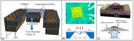
So far, several studies have reported piezoresistive-based accelerometers employing graphene
[132][133][134][201,202,203]. For instance, a piezoresistive transducer was built by using a suspended double-layer graphene ribbon with significant built-in stress (order of 230 to 440 MPa) that shows a noticeable improvement on the static and dynamic characteristics of the device (
Figure 4a)
[132][201]. It was reported the Young’s modulus was decreased for small deflection and applied strain to the device. Moreover, the device has proof mass that is at least three orders of magnitude less than frequently reported piezoresistive silicon accelerometer proof masses that show a greater magnitude of ΔR/R per proof mass volume compared to previously reported piezoresistive accelerometers.
Figure 4. (
a) 3D design of an accelerometer with a suspended graphene ribbons and an attached proof mass
[133][202]. (
b) 1-Optical microscope image of graphene piezoresistors on silicon nitride membrane and the schematic of suspended silicon nitride layer under the applied differential pressure.
Reprinted with permission from ref. [23]. Copyright (
2013) AIP Publishing. (c) Schematic of a suspended graphene cover a circular cavity to measure the chamber pressure due to pressure difference
[53][64].
Likewise, graphene-based suspended, planar, spongy and double layer microstructures have been produced as highly flexible and sensitive pressure sensors. Zhu et al.
[23] fabricated graphene meandering patterns on a square silicon nitride membrane. Pressure applied to the graphene membrane caused it to bend and deform into a concave shape in varying degrees. The graphene sensor’s piezoresistive effect and out-of-plane deflection allowed it to measure the applied pressures. Accordingly, a gauge factor of 1.6 for graphene and a dynamic range from 0 mbar to 700 mbar for the pressure sensor was obtained (
Figure 4b).
Another suspended graphene membrane was fabricated on rectangular and circular cavities (with diameter of 24 μm and depth of 1.5 μm) etched into SiO
2 layer where the membrane was able to deflect due to pressure differences in the sealed cavity and in the pressure chamber. A superior sensitivity in pressure sensing was observed compared to silicon and CNT-based pressure sensors. The maximum GF of the piezoresistive sensor was 4.33 with an average value of 2.92 which, unlike silicon piezoresistive sensors, was unaffected by dopant concentration or crystallographic orientation (
Figure 4c)
[53][64].