Your browser does not fully support modern features. Please upgrade for a smoother experience.
Please note this is a comparison between Version 1 by Dongdong Chen and Version 2 by Dean Liu.
The ADC, a bridge between the analog world and the digital world, converts the analog signals to digital so that the analog signal in the baseband can be processed by the back-end computer or microprocessor.
- analog-to-digital converter
- ultrasonic imaging
- miniaturized system
1. Introduction
Ultrasonic imaging is one of the most widely used imaging methods in nondestructive testing and medical diagnosis due to its advantages of safety, simplicity, cheapness, penetrability, and non-ionization [1][2][3][4][5][6][1,2,3,4,5,6]. Due to the demand of high-resolution medical imaging equipment, ultrasonic imaging systems (UIS) have been rapidly developed and applied in many fields [7][8][9][10][11][12][13][7,8,9,10,11,12,13]. Generally, traditional UIS are expensive, large in size, heavy in mass, and have high power consumption. The miniaturized and portable UIS have been gradually developed and used in a variety of medical conditions such as ambulances, emergency rooms, and remote areas where large-scale ultrasound imaging equipment is not convenient [14][15][16][17][18][14,15,16,17,18]. However, higher resolution imaging is required for the future advanced ultrasonic Doppler imaging, 3D imaging, elastography, etc. The requirement for miniaturized high resolution UIS is urgent, and it has great significance to investigate high-resolution UIS [19][20][21][22][19,20,21,22].
The integrated circuits (ICs) and external devices responsible for signal reception and data conversion have great influence on the comprehensive performance of the UIS. Without compromising imaging quality, the IC with small area, low power consumption, and high precision has become the mainstream trend [23][24][25][26][27][23,24,25,26,27]. A typical UIS receiving chain, as shown in Figure 1, includes analog front-end (AFE), which preprocesses the analog echo signal, and the analog-to-digital converter (ADC), which digitalizes the echo signal for further processing by the digital signal processing (DSP) or microcontroller unit (MCU) [28][29][30][31][32][33][34][28,29,30,31,32,33,34]. The ADC, which realizes the digitalization of the analog echo signals, plays a very important role in the receiving link. Its performance indexes, such as conversion accuracy, speed, linearity, etc., directly affect the quality of UIS. Therefore, according to the urgent requirements of miniaturized high resolution UIS, how to design and fabricate high-performance ADC ICs is very important.
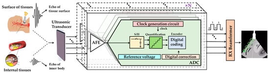
Figure 1. Schematic diagram of ultrasonic imaging receiver chain.
In order to achieve the higher resolution and smaller volume for miniaturized UIS, ADC ICs integrated into the portable imaging terminals or even probes are confronted with high performance requirements:
- (1)ADC is the main power consumption module in the UIS receiving chain. Power consumption exponentially increases with the channel number, and low power consumption becomes one of the main optimization directions of ADC.
- (2)In remote districts, only miniaturized or portable medical equipment is available due to uneven medical development. High integration and small size of receiver link (including ADC) chips are urgently needed for advanced portable or handy UIS devices.
- (3)Advanced UIS typically require high resolution and high-speed A/D data converters to improve ultrasonic imaging quality. Tradeoffs among sampling rate, signal to noise ratio (SNR), occupied area, and power consumption must be carefully considered.
2. ADC for Miniaturized High-Resolution UIS
The ADC, a bridge between the analog world and the digital world, converts the analog signals to digital so that the analog signal in the baseband can be processed by the back-end computer or microprocessor. The accuracy, speed, and linearity of ADC have an important influence on the quality of ultrasonic imaging, and generally, ADC with above 12-bit resolution and tens of MHz sampling rate could meet the performance requirement of traditional UIS. However, higher resolution and speed are desirable for the developed UIS, such as the color Doppler imaging, 3D imaging, and elastography systems.2.1. SAR ADC
The SAR ADC, shown in Figure 3, is a data converter with medium speed and accuracy. The core circuit is generally composed of digital control logic, sample-and-hold circuit (S/H), N-bit register, comparator, and N-bit DAC. Its working process is as follows: the highest bit of the shift register is set as 1, instructing that the DAC outputs the corresponding voltage to the inverting terminal of the comparator for comparison with the input VIN. If VIN is greater than this voltage, the comparator outputs 1, and then the shift register samples and saves the highest bit as 1. Otherwise, it is 0. Until the last bit is compared, the register locks the data and outputs them. Due to adoption of the binary search algorithm, SAR ADC does not need additional coding circuits. In addition, as only one comparator is used in the circuit, it makes the circuit complexity increase slowly with the number of bits, and therefore power consumption and occupied area will be very low. The SAR ADC has become one of the choices of UIS requiring low power and small area A/D convertor.
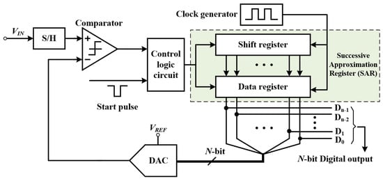
Figure 3. Basic structure diagram of SAR ADC.
2.2. Sigma- Delta ADC
A typical Σ-∆ ADC architecture consists of an analog Σ-∆ modulator (SDM) and a digital decimation filter. The analog SDM can shape the quantization noise and move it to the high frequency domain, and the digital decimation filter, which is implemented by digital circuits, then removes the high frequency noise components. As shown in Figure 8, the working principle of Σ-∆ ADC is: first, the input signal and the output signal of 1-bit or multi-bit DAC are differentiated (represented by ∆) to obtain an analog differential signal, and then the signal is integrated (represented by Σ for integration). After that, the signal is compared with the reference voltage to obtain a 1-bit or multi-bit ADC output. In the low-frequency field, due to the employing of oversampling and noise shaping, Σ-∆ ADC can achieve very high resolution, but with a relatively small bandwidth. These characteristics make it suitable for accurate measurement field and high-resolution ultrasonic imaging. Since the power consumption is directly proportional to the sampling rate, a compromise among the oversampling ratio, SNDR, and power consumption of the Σ-∆ ADC should be considered carefully.
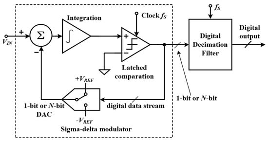
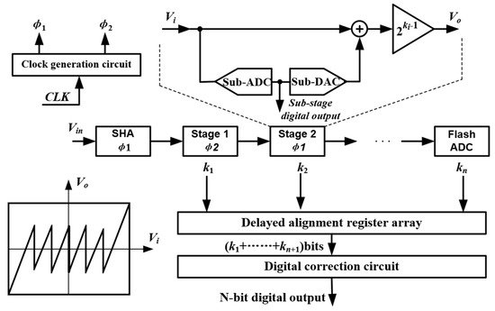
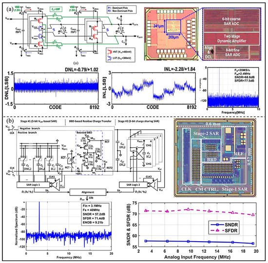
Figure 8. Basic structure diagram of Σ-∆ ADC.
2.3. Pipelined ADC
The pipelined ADC, which is controlled by the two-phase non-overlapping clock, can be understood as a multi-step ADC. Each conversion stage has two working states: the sampling state, and the amplifying and holding state. The working principle of pipelined ADC is as shown in Figure 12: first, the input signal is sampled by a sample/hold amplifier (SHA) circuit and then sent to the pipelined conversion stage where the signal is quantized step by step. The digital correction circuit is used for delay alignment afterwards, and finally an N-bit digital code is obtained. Each sub-stage in the pipelined ADC can work in parallel, and thus the conversion rate of the pipelined ADC can be very high. However, employing of many sub-stages to meet high resolution requirement will certainly lead to higher circuit complexity, and therefore high-power consumption and large occupied area.
Figure 12. Basic structure diagram of pipelined ADC.
2.4. Hybrid ADC
SAR ADC has great advantages in terms of power consumption and low circuit complexity. However, only low-to-medium precision and speed can be achieved because it is quantized in a step-by-step comparison scheme. The Σ-∆ ADC can achieve very high accuracy due to the use of noise shaping and oversampling technology, whereas it is generally slower and can be only used in high-precision and low-speed applications. The developed pipelined ADC can achieve medium precision and high speed, but the use of the excessive number of sub-stages will inevitably result in circuit complexity and high-power consumption. The hybrid ADC is proposed in recent years considering the performance limitations of SAR, Σ-∆ and pipelined ADCs. By combining two or more types of ADCs, performance of the A/D conversion can be improved, and therefore so can the imaging quality of the ultrasound imaging system.
In order to make better use of the advantages of each type of ADC, the hybrid ADCs have been proposed and continuously developed. Kwon et al. [35][63] proposed a closed-loop two-stage dynamic amplifier for pipelined-SAR ADC. The proposed two-stage dynamic amplifier has a high DC gain, and good robustness against process, voltage, and temperature (PVT) variations without further calibration (as shown in Figure 16a). The developed pipelined SAR ADC can achieve a SNDR of 68.8 dB and maintain SNDRs over various sampling rates from 1 to 20 MS/s. The power consumption is only 348 µW from a 1.2 V power supply. To reduce power consumption and improve accuracy, Zhang et al. [36][64] proposed a low-power pipelined-SAR ADC, which adopts the booster barrel brigade device (BBD) to deal with the residual charge, as shown in Figure 16b. However, because the boost BBD introduces large nonlinearity and serious cumulative common mode charge error, a real-time calibration circuit with high power consumption is needed. The SNDR and SFDR of the proposed ADC are 57.1 dB and 71.4 dB, and the power consumption is 1.87 mW.
Figure 16. (a) The proposed chip microphotograph and frequency response comparison of ADC. (Reprinted from [35][63], Copyright 2021, with permission from IEEE); (b) Architecture of the proposed ADC, die microphotograph, and the measured performance. (Reprinted from [36][64], Copyright 2018, with permission from IEEE).