Your browser does not fully support modern features. Please upgrade for a smoother experience.
Please note this is a comparison between Version 2 by Daniel Afzal and Version 1 by Daniel Afzal.
Organic small-molecule semiconductors offer many benefits over their polymer equivalents, including ease of production, greater purity, and increased charge carrier mobility [44,45,46,47]. OFETs based on small-molecule semiconductors have been intensively investigated as sensors for a variety of applications, including gas sensing, chemical sensing, biosensors, and pressure sensing [48,49,50].
- organic field effect transistor
- organic thin film transistor
1. OFET Semiconductor Channel as Sensing Element
Pentacene is one of the most commonly used semiconducting layers in OFET devices for various applications [1,2,3,4]. Jung et al. report an OTFT temperature sensor using pentacene as the semiconducting layer on a flexible polyethylene naphthalate (PEN) film for administering point-of-care diagnoses [39]. A 50 nm pentacene film was deposited on top of a polyvinylphenol (PVP) gate dielectric. When the device is measured between 0 and 80 °C, the IDS increases with increasing temperature. This IDS modulation is mainly due to the positive shift of the VT, so the most significant increase in current is observed in the subthreshold region with a linear increase from ~10−10 A at 0 °C to ~10−8 A at 80 °C.
Copper phthalocyamine (CuPc) and fluorinated copper phthalocyanine (F16CuPc) are widely studied p-type and n-type small-molecule semiconductors for OFETs because of their good carrier mobility and environmental stability. CuPc and F16CuPc exhibit a weak dependence of µsat on temperature around room temperature, each having an Ea of 73 and 39 meV [7,8], respectively, which are similar to that of pentacene [5,6]. Therefore, IDS in the saturation region of OFETs based on these materials would also be weakly dependent on temperature and not suitable as the signal output of temperature sensors around room temperature. Consequently, Boileau et al. used the VT response to the temperature of OFETs based on CuPc and F16-CuPC for DNA sensing [9]. The goal was to design an accurate temperature sensor working in the optimal temperature range (40 to 70 °C) where DNA binding occurs. The authors observed that the hole and electron mobilities (µh and µe) of CuPc and F16CuPc increase with temperature with coefficients of 1%/°C and 0.1%/°C, respectively, in the temperature range of 25 to 90 °C. On the other hand, the VT changes significantly from −7.6 V to −1.8 V with a change rate of 0.11 V/°C for CuPc. For the n-type F16CuPc-based OFET, the VT changes to the negative direction from −9.9 V to −26.4 V with a charge rate of −0.25 V/°C, indicating its better sensitivity than the CuPc device. The opposite VT shift directions and different sensitivities observed for the two semiconductors may be due to their different carriers (holes and electrons) associated with different carrier traps at the interface between the semiconductor and the dielectric.
To improve the temperature sensitivity of F16CuPc-based OFETs, Ye et al. developed an OFET device using a pn heterojunction layer of α-sexithiophene (α6T)/F16CuPC [10]. Specifically, a layer of p-type semiconductor α6T was deposited on top of the F16CuPC semiconducting layer and the source/drain electrodes (Figure 5). It has been reported that the use of a pn heterojunction active channel layer in OFETs can realize ambipolar charge transport characteristics and/or improve charge carrier mobility [11,12,13,14,15]. In particular, the VT is a function of the thickness of the top layer in the pn heterojunction [16], which may allow the use of VT as the sensitivity parameter of the OFET temperature sensor in a more controllable manner. The authors found that when the thickness of the α6T layer increased from 0 nm to ~5–7 nm, VT changed significantly from 23.13 V to 18.10 V, and then stabilized. In the linear regime (|VDS| < |VGS − VT|), the OFET with α6T (20 nm)/F16CuPC (50 nm) displayed a linear log(IDS)-versus-T relationship: log(ID)=kT+c0 in the temperature range of 100 to 300 K (Figure 5a), which is gate voltage-dependent. The slope k increases with VGS first, reaching the maximum value of 0.11 dec/°C at VGS = 5 V (most sensitive), and then drops rapidly with further increasing VGS (Figure 5b). As shown in Figure 5c, µ follows a thermally activated Arrhenius behaviour (μ∝exp(−Ea/kBT)) with two distinct temperature ranges. The activation energy Ea is 40.1 meV above 200 K and drops to 16.3 meV in the lower temperature range of 100 to 200 K. The device also showed linear temperature dependence of VT with different slopes in the two temperature ranges (Figure 5d). In the range of 100 to 200 K, the sensitivity (ΔVT/ΔT) is −0.90 V/°C, and between 200 K and 300 K, the sensitivity is −0.185 V/°C. These two regions are attributed to two different mechanisms dominating in each region. The charge transport in the lower temperature range is dominated by the MTR mechanism, while the charge transport in the higher temperature range is dominated by the thermal enhancement of the hopping transport or VRH. These sensitivities are higher than those of a previously reported OFET with a similar structure with only F16CuPC (−0.02 V/°C) [8], indicating the beneficial effect of using a pn heterojunction structure to improve the sensitivity of the sensor.
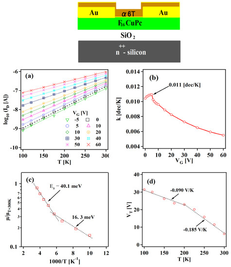
Figure 5. (a) Dependence of log (IDS) on the temperatures at different VGS, (b) dependence of k on VGS in log(IDS)=kT+c0 obtained from data in (a), (c) temperature dependence of µ, and (d) temperature dependence of VT of the α6T (20 nm)/F16CuPc (50 nm) OFET device in the linear regime. Reproduced with permission from [10] Scientific Research, 2016. Note: ID and VG in (a) are IDS and VGS, respectively.
An organic-inorganic hybrid perovskite-based ambipolar FET temperature sensor was reported by Haque et al. recently [17]. The active MAPbI3 layer is fabricated using a stoichiometric mixture of powdered methylammonium iodide (MAI) and lead iodide (PbI2). The OTFT exhibited excellent air stability without the need for an encapsulation layer. The charge transport obeys the MTR mechanism where traps, mostly localized in the grain boundaries, have energy levels close to the conduction band, and the trapped electrons can be easily released into the conduction band by thermal energy. The temperature dependence of VT was used as the sensitivity parameter for the device. The VT shows a linear relationship with temperature in the range of 29 to 45 °C with a temperature coefficient value of 200 mV/°C, which is higher than the values reported for inorganic semiconductor-based FET temperature sensors. It was found that maintaining a stoichiometric ratio of MAI and PbI2 is critical to achieving high sensitivity. The devices with the PbI2-rich and MAI-rich films exhibited much lower temperature coefficients of 12 and 100 mV/°C, respectively, since unreacted PbI2 and MAI can reduce carrier traps.
2. OFET Dielectric Layer as Sensing Element
Insulating polymers are often used as dielectric materials in OFETs due to their compatibility with flexible substrates and solution processibility via spin coating, casting, and printing under ambient conditions [18]. Moreover, as with the polymer semiconductors, the structure and functionality of the polymer dielectric can be tuned to meet the requirements of the device. In particular, the properties of some polymer dielectrics are more temperature-dependent than organic semiconductors, so they can be used as sensing elements for OFET temperature sensors.
Polylactide (PLA) was used as the polar material that serves both as a flexible substrate and as a gate dielectric for the device with both n- and p-type small-molecule semiconducting active layers. Specifically, three-arm stereocomplex PLA (tascPLA) was synthesized from the ring-opening polymerization of D-lactide and used for these devices. The MTR mechanism can describe the role that the dielectric plays in temperature sensing. At the interface, PLA induces multiple charge carrier traps with varying energy levels, which decreases the carrier concentration. As the temperature increases, the thermal energy can release carriers from these traps and thus modulate the IDS response. The DNTT-tascPLA-OFET shows a much stronger response in IDS with temperature in the range of 25 to 150 °C compared to the device using SiO2 as the dielectric (Figure 6a,b), indicating the high thermal sensitivity of PLA. The device showed excellent cycling stability at 100 °C (Figure 6c,d). Mobility and VT also show high sensitivities to temperature (Figure 6e,f).
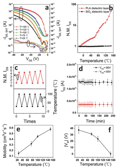
Figure 6. Temperature sensitivity of DNTT-tascPLA-OFETs: (a) transfer characteristics of DNTT-tascPLA-OFET (VDS = −60 V) at different temperatures, (b) normalized (N.M.) IDS at different temperatures of the OFETs with tascPLA or SiO2 dielectric layers, (c) normalized IDS of the DNTT-tascPLA-OFET measured between two temperatures of 25 and 100 °C, (d) IDS of the tascPLA–OFETs maintained at 100 °C as a function of time at VDS = −80 V at two different VGS, and (e) µ and (f) VT of the DNTT-tascPLA-OFETs at different temperatures. Reproduced with permission from [40] Wiley-VCH, 2015.
Subbarao et al. used CuPc as the semiconducting layer in conjunction with a tri-layer dielectric system where the polar PVA layer is deposited between a layer of poly(methyl methacrylate) (PMMA) and a layer of Al2O3 [19]. The sensor results displayed two distinct linear trends in the ranges of 240 to 300 K and 300 to 370 K with sensitivities of 0.45 nA/°C and 8 nA/°C, respectively. Below 300 K it can be assumed that the VRH mechanism dominates over the MTR mechanism, while above 300 K the opposite occurs. The device showed a quite fast response and recovery times of 25 and 15 s, respectively. The response and recovery times included the time to mechanically switch between temperatures, and the actual sensor response and recovery times are expected to be much faster [19].
Mandal et al. incorporated hexagonal barium titanate nanocrystals (h-BTNCs) as a dielectric film and pentacene as the channel layer to fabricate ultrafast, flexible OFET temperature sensor devices [20]. The perovskite BaTiO3 is a ferroelectric material with its ferroelectric property originating from the crystal structure distortion upon temperature change. The BaTiO3 film synthesized by the traditional high-temperature process is very rough, which will have a negative impact on the current at the semiconductor/dielectric interface. Furthermore, the perovskite BaTiO3 only shows ferroelectric properties at low temperatures. To circumvent these issues, the authors developed a low-temperature (~60 °C) process to prepare h-BTNCs. Thin films of h-BTNCs with very smooth surfaces can be obtained simply by spin coating. A series of OFETs with a bilayer dielectric of h-BTNC (55 nm) on Al2O3 (15 nm), a pentacene semiconductor layer, Cu source, and drain electrodes were fabricated on a thin Al-coated poly(ethylene terephthalate) (PET) substrate (10 μm), where the Al layer is the gate electrode. The devices were encapsulated with a PDMS layer. The OFETs had a low operating voltage of 1.5 V and achieved a high mobility of 1.46 cm2/(V·s). When the device was used as a temperature sensor, it showed a linear dependence of IDS on temperature with a slope (sensitivity) of 20 nA/°C between 27 and 45 °C. The greatly enhanced sensitivity is mainly due to the use of the h-BTNC layer since the contributions of pentacene, and other layers are very small. The flexibility of the device was also evaluated, and the sensor maintained a stable response with a minimal level of hysteresis in the temperature range when subjected to bending with a radius of 4 mm. The device was used to monitor the temperature changes of the air inhaled and exhaled through the nose a few cm from the device. Rapid response and recovery times of 24 and 51 ms, respectively, were achieved.
Rullyani et al. reported the use of poly(N-isopropylacrylamide) (PNIPAM) as a thermoresponsive polymer dielectric for OFET sensors [21]. The PNIPAM layer undergoes reversible phase transitions above its lower critical solution temperature of 32 °C. These transitions enhance the charge transport in the semiconducting layer (pentacene in this case) due to an improved semiconductor/dielectric interface with increasing temperature. The sensor was evaluated between 30 and 45 °C with a sensitivity of 2.58 µA/°C with the IDS being on the order of microamperes. The device is suitable for sensing the human body temperatures.
3. Thermistor as Sensing Element
As aforementioned, IDS is a preferred parameter as an output signal of OFET temperature sensors because of its high reliability, but its temperature dependence is weak. On the other hand, VT has strong temperature dependence, but it is affected by numerous factors in the fabrication process and the device operating environment. To solve this issue, thermistors, whose resistance changes notably with temperature, have been integrated with OFETs to make temperature sensors with high sensitivity.
Ren et al. [42] integrated a thermistor with an OFET to improve the dependence of IDS on temperature (Figure 7), and used dynamic range (DR) to present the sensitivity of the device. The thermistor consists of pentacene film embedded with Ag nanoparticles and two electrodes. One electrode of the thermistor is connected to the gate of the pentacene-based OTFT, so the gate bias of the OFET can be modulated by the resistance of the thermistor. Ag nanoparticles act as charge traps, so the conductivity activation energy of the thermistor film is increased to 361 meV compared with pure pentacene (157 meV). This results in a stronger dependence of the conductivity on the temperature of the thermistor film.
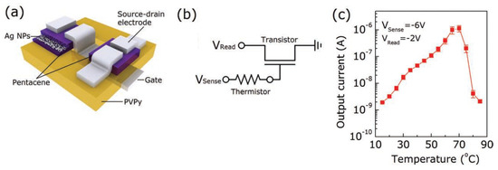
Figure 7. (a) The schematic diagram of the transistor–thermistor temperature sensor; (b) The circuit of temperature sensor; (c) IDS response to temperature of the transistor-thermistor device. Reproduced with permission from [42] Wiley-VCH, 2013.
The integrated temperature sensor device shows almost three orders of magnitude increase in IDS with temperature when measured between 15 and 70 °C with a measurement step of 5 °C. The sensitivity of the temperature sensor is represented by the DR, which is the ratio between the maximum and minimum changes of IDS at a specific temperature (T) with reference to the lowest temperature (15 °C): DR = ΔIT,max/ΔIT,min, where ΔIT = IT − I15. A higher DR implies a more sensitive device. This device had a DR of 10 bits (102), which is the highest value reported among organic temperature sensors. The sensitivity of the device deteriorates rapidly above 70 °C, which may be due to the evaporation of water absorbed by the polyvinylpyrrolidone (PVPy) dielectric layer at high temperatures, resulting in a decrease in capacitance.
The same research group reported a flexible low operating power 16 × 16 active-matrix OFET temperature sensor array by adopting a similar device design [22]. A high-performance p-type semiconductor dinaphtho[2,3-b:2′,3′-f]thieno[3,2-b]thiophene (DNTT) was used as the active layer in the OFET device. An Al2O3 dielectric layer was used to decrease leakage current down to ~50 pA. A thermistor consisting of an Ag nanoparticles-doped pentacene film active layer was connected to the DNTT-OFET. The array fabricated on an ultrathin (12 μm) PET substrate can be operated at low voltages below 4 V. In the temperature range between 20 and 100 °C, the array achieved a temperature resolution of 0.4 °C and a TCR of −4.4%/°C. The device maintained its integrity after 10,000 bending cycles, and the array was able to provide excellent 2D spatial resolution. The superb flexibility and durability of the sensor array make it suitable for conformal temperature measurement of objects with irregular and varied surface geometry such as flexible electronic products and human bodies.
Temperature and pressure sensor arrays are of great interest because of their potential for artificial skin applications with spatial resolution. Yokota et al. copolymerized butyl acrylate with octadecyl acrylate P (BA-OA) and added 25% graphite filler particles to fabricate positive temperature coefficient (PTC) thermistor sensors [23]. The PTC sensors were integrated with OFETs to create a 12 × 12 active-matrix sensor array on a polyimide substrate, where an anodized aluminum oxide layer modified by a phosphonic acid self-assembled monolayer (SAM) was used as the gate dielectric, and a 30 nm DNTT layer was used as the semiconductor later in OFETs. This ultra-flexible sensor array was able to accurately measure temperature shifts after being placed between two lobes of a live rat lung, where small temperature fluctuations occur due to respiration. The array performed well between 29.8 and 37.0 °C with minimal hysteresis (1 °C) and a spatial resolution of 5 mm. Furthermore, the device had a rapid response time of 100 ms and remained stable for 1800 thermal cycles within the operating temperature range.
A recent work by Ishaku and Gleskova reported a temperature sensor with a DNTT-OFET connected to a commercially available thermistor with a negative temperature coefficient (NTC) [24]. The OFET included a dielectric of aluminum oxide (AlOx) with an octadecylphosphonic acid (C18PA) SAM for low voltage operation. Previous works have reported using C18PA to improve the µsat of charge carriers in OTFTs by inducing edge-on orientation of the semiconducting layer [25]. The integrated OFET-sensor was evaluated between 20 and 50 °C with the thermistor modulating the gate voltage. A low operational voltage of −7 V and a TCR of −2.44%/°C were achieved.
Nakayama et al. reported two types of organic temperature sensing devices using a combination of p- and n-type semiconductors to fabricate analog-to-digital converter (ADC) OFETs [26]. The organic semiconductor layers of 3,11-didecyldinaphtho[2,3-d:2′,3′-d’]benzo[1,2-b:4,5-b’]dithiophene (C10-DNBDT) and GSID 104031-1 (BASF SE) for p- and n-type OFETs, respectively, were solution-processed. A unit consisting of a complementary metal-oxide semiconductor (CMOS) comparator and an inverter made of the p- and n-channel OFET devices is connected to a temperature sensor unit composed of two PEDOT: PSS resistors (TCR of −0.87%/°C) and two Cr/Au resistors (TCR: 0.064%/°C) to form a temperature detector. The temperature detector can produce a binary digital (1-bit) readout depending on whether the temperature was above a designated threshold value (Tth). The authors further fabricated a 2-bit parallel ADC composed of three comparators and one temperature sensor unit for more detailed temperature detection. The 2-bit ADC can have four output combinations, (0,0,0), (0,0,1), (0,1,1), (1,1,1), corresponding to the temperature ranges of <33 °C, 33–50 °C, 50–67 °C, and >67 °C, respectively. Such digital signals can be easily read with common radio-frequency identification (RFID) readers.
4. Other Types of Sensing Elements
Someya et al. reported a large-area network of temperature and pressure sensors on a flexible plastic substrate using organic semiconductors [41]. The temperature sensor cell consists of an organic diode as the temperature sensing element and an OFET. The OFET device is composed of a pentacene semiconductor layer, a polyimide dielectric layer, and Au source, drain, and gate electrodes. The organic diode has a structure of PET/ITO/CuPc (30 nm)/PTCDI (50 nm)/Au, where PTCDI (3,4,9,10-perylenetetracarboxylic diimide) is an n-type semiconductor, forming a pn heterojunction with the p-type CuPc. The pn heterojunction layer has a much stronger temperature dependence than CuPc or PTCDI alone. Therefore, this organic diode functions as a sensing element. The magnitude of IDS of the temperature sensor cell increases markedly from ~0.4 μA to ~1.4 μA in the range of 30 to 80 °C or ~20 nA/°C.
Developing polymer composites is a method to improve the electrical properties of polymer materials. The interactions between the polymer and the organic/inorganic material in the polymer matrix can lead to higher sensitivity and better overall performance in sensors [28]. Polymer materials can also be used as a matrix to embed active materials to take advantage of polymer properties, such as processability and stability, for organic electronic applications. In 2009, Graz et al. [29] incorporated lead titanate (PbTiO3) nanoparticles into the matrix of ferroelectric P (VDF-TrFE). A two-step polarization process is used to polarize the foil made of this composite material, so that some areas of the PbTO3 nanoparticles and the polymer matrix have parallel polarization directions, while other areas have anti-parallel polarization directions. Areas with parallel polarization directions are pyroelectric, while areas with anti-parallel polarization directions are piezoelectric. The composite foil was laminated to amorphous silicon (a-Si) TFTs on their polyimide gate dielectric substrate in the adjacent parallel and anti-parallel polarization directions, respectively. The IDS of a TFT is modulated pyro- or piezoelectrically depending on the polarization directions of the composite foil area. The device significantly reduced cross-sensitivity between the piezoelectric and pyroelectric effects and displayed a linear relationship correlated to temperature.
Sensor devices can be connected to one of the electrodes of an OFET and their response to the target analyte can be used to modulate a characteristic of the OFET device that changes the output signal of the OFET. In 2014, Cosseddu et al. introduced a temperature sensor based on an organic charge modulated field-effect transistor (OCMFET) using the pyroelectric poly(vinylidene difluoride) (PVDF) [43]. The polymer film forms the dielectric layer of a parallel plate capacitor, which is connected to the floating gate of an OFET device. Temperature modulations affect the charge separation in the PVDF layer, which modulates the carrier concentration that directly correlates to the IDS response of the sensor. Calibration curves of ΔIDS–T for this temperature sensor were established within a working range of 10 to 42 °C.
Table 1 summarizes the OFET-based temperature sensors using the small-molecule materials discussed in this section organized by sensing the elements and reporting the OFET channel material, working range, output signal, and the reported sensitivity of each device.
Table 1. Summary of small-molecule OFET temperature sensors.
| Sensor Structure | OFET Channel | Sensing Element | Working Range | Sensor Parameter | Sensitivity | Year [Ref.] |
|---|---|---|---|---|---|---|
| Sensing element: OFET active layer | ||||||
| OFET | Pentacene | OFET channel | 0–80 °C | IDS,sub | ~0.1 nA/°C 1 | 2006 [39] |
| OFET | Pentacene | OFET channel | 0–180 °C | IDS,sub, VT | - | 2007 [5] |
| OFET | CuPc | OFET channel | 25–90 °C | VT | 0.11 V/°C | 2019 [9] |
| OFET | F16CuPc | OFET channel | 25–90 °C | VT | −0.25 V/°C | 2019 [22] |
| OFET | α6T/F16CuPc pn junction |
OFET channel | −173–27 °C | VT | −0.090 V/°C (<–73 °C) −0.185 V/°C (>–73 °C) |
2016 [10] |
| Organic-inorganic FET | MAPbI3 | FET channel | 20–45 °C | VT | −200 mV/°C | 2020 [17] |
| Sensing element: dielectric layer | ||||||
| OFET | 6PTTP6 8-3-NTCDI DNTT |
Dielectric (PLA) |
−25–200 °C | IDS | 0.29 μA/°C 1 | 2015 [40] |
| OFET | CuPc | Dielectric (PVA) |
−20–0 °C | IDS | 0.45 nA/°C (<300 K) 8 nA/°C (>300 K) |
2018 [19] |
| OFET | Pentacene | Dielectric (h-BTNC) |
27–45 °C | IDS | 20 nA/°C | 2019 [20] |
| OFET | Pentacene | Dielectric (PNIPAM) |
30–45 °C | IDS | 2.58 µA/°C | 2020 [21] |
| Sensing element: thermistor | ||||||
| OFET-thermistor | Pentacene | Thermistor (Pentacene/AgNPs) | 15–70 °C | IDS | DR = 10 bits | 2013 [42] |
| OFET-thermistor | DNTT | Thermistor (Pentacene/AgNPs) | 20–100 °C | TCR | −4.40%/°C | 2016 [22] |
| OFET-thermistor | DNTT | PTC thermistor (copolymer-graphite) |
29.8–37.0 °C | IDS or R | 20 mK | 2015 [23] |
| OFET-thermistor | DNTT | Thermistor (commercial) | 20–50 °C | TCR | −2.44%/°C | 2021 [24] |
| OFET-thermistor ADC |
C10-DNBDT (p) GSID 104031-1 (n) |
Thermistors (PEDOT:PSS; Cr/Au) |
33–67 °C | Binary codes | - | 2016 [26] |
| Sensing element: other types | ||||||
| OFET-diode | Pentacene | Diode (CuPc/PTCDI) |
30–80 °C | IDS | ~20 nA/°C | 2005 [41] |
| OFET-diode | Pentacene | OFET& Diode |
27.2–59.0 °C | VDS | 16.3 mV/°C | 2013 [27] |
| OFET-capacitor | Pentacene | Capacitor (polymer composite) |
~r. t. | IDS | ~30 nA/°C 1 | 2009 [29] |
| OFET-capacitor | TIPS | Pyroelectric (PVDF) |
10–42 °C | IDS | ~0.14 μA/°C 1 | 2014 [43] |
References
- Baeg, K.-J.; Noh, Y.-Y.; Ghim, J.; Kang, S.-J.; Lee, H.; Kim, D.-Y. Organic Non-Volatile Memory Based on Pentacene Field-Effect Transistors Using a Polymeric Gate Electret. Adv. Mater. 2006, 18, 3179–3183.
- Schroeder, R.; Majewski, L.A.; Grell, M. A Study of the Threshold Voltage in Pentacene Organic Field-Effect Transistors. Appl. Phys. Lett. 2003, 83, 3201–3203.
- Shi, W.; Yu, J.; Katz, H.E. Sensitive and Selective Pentacene-Guanine Field-Effect Transistor Sensing of Nitrogen Dioxide and Interferent Vapor Analytes. Sens. Actuators B Chem. 2018, 254, 940–948.
- Wang, Y.; Kang, L.; Liu, Z.; Wan, Z.; Yin, J.; Gao, X.; Xia, Y.; Liu, Z. Enhancement of Memory Properties of Pentacene Field-Effect Transistor by the Reconstruction of an Inner Vertical Electric Field with an n-Type Semiconductor Interlayer. ACS Appl. Mater. Interfaces 2021, 13, 13452–13458.
- Jung, S.; Ji, T.; Varadan, V.K. Temperature Sensor Using Thermal Transport Properties in the Subthreshold Regime of an Organic Thin Film Transistor. Appl. Phys. Lett. 2007, 90, 062105.
- Kawakami, D.; Yasutake, Y.; Nishizawa, H.; Majima, Y. Bias Stress Induced Threshold Voltage Shift in Pentacene Thin-Film Transistors. Jpn. J. Appl. Phys. 2006, 45, L1127–L1129.
- Kwak, T.H.; Kang, H.S.; Kim, K.; Cho, M.Y.; Lee, J.W.; Joo, J. Copper-Phthalocyanine Based Organic Thin Film Transistor. In Proceedings of the 2006 IEEE Nanotechnology Materials and Devices Conference, Gyeongju, Korea, 22–25 October 2006; pp. 630–631.
- Ye, R.; Baba, M.; Ohishi, Y.; Mori, K.; Suzuki, K. On the Correlation between Morphology and Electronic Properties of Fluorinated Copper Phthalocyanine (F16CuPc) Thin Films. Mol. Cryst. Liq. Cryst. 2006, 444, 203–210.
- Boileau, N.T.; Melville, O.A.; Mirka, B.; Cranston, R.; Lessard, B.H. P and N Type Copper Phthalocyanines as Effective Semiconductors in Organic Thin-Film Transistor Based DNA Biosensors at Elevated Temperatures. RSC Adv. 2019, 9, 2133–2142.
- Ye, R.; Ohta, K.; Baba, M. Temperature Dependence of Electrical Properties of Organic Thin Film Transistors Based on Pn Heterojuction and Their Applications in Temperature Sensors. J. Comput. Commun. 2016, 4, 10–15.
- Ye, R.; Baba, M.; Oishi, Y.; Mori, K.; Suzuki, K. Air-Stable Ambipolar Organic Thin-Film Transistors Based on an Organic Homostructure. Appl. Phys. Lett. 2005, 86, 253505.
- Ye, R.; Baba, M.; Suzuki, K.; Mori, K. Improved Performance of Fluorinated Copper Phthalocyanine Thin Film Transistors Using an Organic Pn Junction: Effect of Copper Phthalocyanine Film Thickness. Thin Solid Film. 2009, 517, 3001–3004.
- Wang, J.; Wang, H.; Yan, X.; Huang, H.; Yan, D. Organic Heterojunction and Its Application for Double Channel Field-Effect Transistors. Appl. Phys. Lett. 2005, 87, 093507.
- Xiang, L.; Ying, J.; Han, J.; Zhang, L.; Wang, W. High Reliable and Stable Organic Field-Effect Transistor Nonvolatile Memory with a Poly(4-Vinyl Phenol) Charge Trapping Layer Based on a Pn-Heterojunction Active Layer. Appl. Phys. Lett. 2016, 108, 173301.
- Yu, S.H.; Kang, B.; An, G.; Kim, B.; Lee, M.H.; Kang, M.S.; Kim, H.; Lee, J.H.; Lee, S.; Cho, K.; et al. Pn-Heterojunction Effects of Perylene Tetracarboxylic Diimide Derivatives on Pentacene Field-Effect Transistor. ACS Appl. Mater. Interfaces 2015, 7, 2025–2031.
- Ye, R.; Ohta, K.; Baba, M. In-Situ Study of Pn-Heterojunction Interface States in Organic Thin Film Transistors. Thin Solid Film. 2014, 554, 137–140.
- Haque, F.; Lim, S.; Lee, S.; Park, Y.; Mativenga, M. Highly Sensitive and Ambient Air-Processed Hybrid Perovskite TFT Temperature Sensor. IEEE Electron Device Lett. 2020, 41, 1086–1089.
- Shao, M.; He, Y.; Hong, K.; Rouleau, C.M.; Geohegan, D.B.; Xiao, K. A Water-Soluble Polythiophene for Organic Field-Effect Transistors. Polym. Chem. 2013, 4, 5270.
- Subbarao, N.V.V.; Mandal, S.; Gedda, M.; Iyer, P.K.; Goswami, D.K. Effect of Temperature on Hysteresis of Dipolar Dielec tric Layer Based Organic Field-Effect Transistors: A Temperature Sensing Mechanism. Sens. Actuators A Phys. 2018, 269, 491–499.
- Mandal, S.; Banerjee, M.; Roy, S.; Mandal, A.; Ghosh, A.; Satpati, B.; Goswami, D.K. Organic Field-Effect Transistor-Based Ultrafast, Flexible, Physiological-Temperature Sensors with Hexagonal Barium Titanate Nanocrystals in Amorphous Matrix as Sensing Material. ACS Appl. Mater. Interfaces 2019, 11, 4193–4202.
- Rullyani, C.; Singh, M.; Li, S.-H.; Sung, C.-F.; Lin, H.-C.; Chu, C.-W. Stimuli-Responsive Polymer as Gate Dielectric for Organic Transistor Sensors. Org. Electron. 2020, 85, 105818. [CrossRef]
- Ren, X.; Pei, K.; Peng, B.; Zhang, Z.; Wang, Z.; Wang, X.; Chan, P.K.L. A Low-Operating-Power and Flexible Active-Matrix Organic-Transistor Temperature-Sensor Array. Adv. Mater. 2016, 28, 4832–4838.
- Yokota, T.; Inoue, Y.; Terakawa, Y.; Reeder, J.; Kaltenbrunner, M.; Ware, T.; Yang, K.; Mabuchi, K.; Murakawa, T.; Sekino, M.; et al. Ultraflexible, Large-Area, Physiological Temperature Sensors for Multipoint Measurements. Proc. Natl. Acad. Sci. USA 2015, 112, 14533–14538.
- Ishaku, A.A.; Gleskova, H. Potential of Low-Voltage Organic Transistors with High on-State Drain Current for Temperature Sensor Development. Org. Electron. 2021, 93, 106152.
- Jang, S.; Son, D.; Hwang, S.; Kang, M.; Lee, S.-K.; Jeon, D.-Y.; Bae, S.; Lee, S.H.; Lee, D.S.; Kim, T.-W. Hybrid Dielectrics Composed of Al2O3 and Phosphonic Acid Self-Assembled Monolayers for Performance Improvement in Low Voltage Organic Field Effect Transistors. Nano Converg. 2018, 5, 20.
- Nakayama, K.; Cha, B.-S.; Kanaoka, Y.; Isahaya, N.; Omori, M.; Uno, M.; Takeya, J. Organic Temperature Sensors and Organic Analog-to-Digital Converters Based on p-Type and n-Type Organic Transistors. Org. Electron. 2016, 36, 148–152.
- Ozgun, R.; Katz, H.E.; Andreou, A.G. Organic Diode Implementations in Configurable Architectures and Temperature Sensors. In Proceedings of the 2013 Microsystems for Measurement and Instrumentation: Fulfilling the Promise (MAMNA), Gaithersburg, MD, USA, 14 May 2013; pp. 24–27.
- Dudhe, R.S.; Sinha, J.; Kumar, A.; Rao, V.R. Polymer Composite-Based OFET Sensor with Improved Sensitivity towards Nitro Based Explosive Vapors. Sens. Actuators B Chem. 2010, 148, 158–165.
- Graz, I.; Krause, M.; Bauer-Gogonea, S.; Bauer, S.; Lacour, S.P.; Ploss, B.; Zirkl, M.; Stadlober, B.; Wagner, S. Flexible Active-Matrix Cells with Selectively Poled Bifunctional Polymer-Ceramic Nanocomposite for Pressure and Temperature Sensing Skin. J. Appl. Phys. 2009, 106, 034503.
More