GlNot sass technologies for 3D printing can be divided into several categories according to thetisfied with the current stage of the extensive research on 3D printing method and the form of pre-treatment for the raw materials. These categories include powder-based, photopolymerization-based, and material extrusion-basedtechnology for polymers and metals, researchers are searching for more innovative 3D printing technology. Among them, fused deposition modeling (FDM), based on material extrusion (MEX), and selective laser sintering/melting (SLS/SLM), based on powder, usually require stricties for glass fabrication in what has become the latest trend of interest. The traditional glass manufacturing processing conditions and are therefore less suitable for laboratory processing. The most promis requires complex high-temperature melting and casting processing technologies are stereolithography (SLA), digital light processing (DLP), two-photon polymerizes, which presents a great challenge to the fabrication (TPP), sheet lamination (SL), which is based on photopolymerization, and DIW, based on MEXof arbitrarily complex glass devices. The emergence of 3D printing technology provides a good solution.
1. Introduction
Additive manufacturing (AM) is defined as “the process of manufacturing objects layer by layer by connecting materials through 3D model data”, which is also known as the additive manufacturing process and free-form fabrication
[1]. Additive manufacturing was first invented and developed in the 1980s and, since then, the technology has gained traction thanks to its rapid, mold-less molding, as well as its relatively short cycle of manufacturing and the ability to replicate accurately. Over the next few years, the technologies associated with additive manufacturing (AM) will rapidly evolve and transform into a more comprehensive manufacturing approach. In addition, additive manufacturing has an extremely high material utilization rate compared with traditional manufacturing processes, which helps to achieve satisfactory geometric precision
[2]. All these unique features have led to a greater diversity of materials produced using additive manufacturing techniques, including even polymers
[3], metals
[4][5][4,5], soft matter
[6], and nanocomposites. The great complexity of geometries in additive manufacturing has been widely used in aerospace, energy storage, and optical precision instruments
[7], and it has even demonstrated some exceptional capabilities and potential for rapid response to public health emergencies
[8].
Currently, additive manufacturing technology is also extensively applied to the manufacturing of polymer and metal objects
[9][10][11][12][9,10,11,12]. The application of glass materials to 3D printing technology is not yet widespread due to their high melting point and high hardness characteristics. Glass materials have shown great applicability in optical devices given their many important assets, such as unparalleled optical transparency and excellent physical as well as chemical properties. However, the traditional manufacturing methods for glass are time consuming and labor intensive, and glass cannot be precisely molded. The process of molding glass is still being explored. Despite the hardships, 3D printing technology with photocuring and high-temperature sintering and other processing methods are now available to process glass materials
[13][14][15][16][17][18][19][20][13,14,15,16,17,18,19,20]. The 3D printing glass field has been widely concerned with improvement and has been increasingly recognized year by year, and it is now understood to be very valuable for research in the future.
Glass technologies for 3D printing can be divided into several categories according to the printing method and the form of pre-treatment for the raw materials. These categories include powder-based, photopolymerization-based, and material extrusion-based 3D printing technology, as shown in Table 1. Among them, fused deposition modeling (FDM), based on material extrusion (MEX), and selective laser sintering/melting (SLS/SLM), based on powder, usually require strict processing conditions and are therefore less suitable for laboratory processing. The most promising processing technologies are stereolithography (SLA), digital light processing (DLP), two-photon polymerization (TPP), sheet lamination (SL), which is based on photopolymerization, and DIW, based on MEX.
Table 1.
Glass 3D printing technologies.
| Categories |
Glass 3D Printing Technology Type |
Abbreviation |
| Powder based |
Selective laser sintering |
SLS |
| |
Selective laser melting |
SLM |
| Photopolymerization based |
Stereolithography |
SLA |
| |
Two-photon polymerization |
TPP |
| |
Digital light processing |
DLP |
| |
Sheet lamination |
SL |
| Material extrusion based |
Direct ink writing |
DIW |
| |
Fused deposition modeling |
FDM |
So far, time-consuming and expensive customization, low dimensional precision, and rough surface finish are the main challenges in the process of glass fabrication through 3D printing technology
[21][22][23][21,22,23]. The purpose of this
re
ntryview is to discuss the latest state of 3D printing technologies for fabricating glass. The
entrypaper provides an overview of the development of popular technologies, describes general methods for preparing glass with 3D printing technology, gives representative examples of applications, and compares important aspects of glass 3D printing technology. Finally, future challenges and opportunities for glass 3D printing technology are envisioned and discussed in order to achieve wider applications.
2. Classification of 3D Printing Glass Technologies
In recent years, more than 50 types of 3D printing technologies based on different principles have been developed according to the different requirements of materials, printing speed, and printing precision
[24]. Only the following technologies have been reported for glass fabrication: SLS/SLM, FDM, SLA, DLP, TPP, and DIW, as well as SL. Among them, although FDM is mostly used to prepare glass crafts due to the characteristics of the processing technology, it cannot be widely used in the optical field
[25][26][27][25,26,27]. While the SLS/SLM technique provides good control of the crystal structure and achieves nearly 100% material utilization
[24], the processing process generates vapor bubbles, which limits the optical transparency of the glass. In addition, Luo et al. proposed a method to produce silica glass using the fiber feeding method. However, although the initially prepared samples had some transparency, a tedious polishing process was required to achieve high transparency properties
[28][29][30][28,29,30]. This has limited the development of this technology in the optical field.
Therefore, in terms of the efficiency and practicality of glass microstructure preparation, the 3D printing methods that can be used to prepare glass microstructures are mainly of two main types: (1) four methods based on photopolymerization with “liquid glass” materials
[13][31][32][33][34][35][13,31,32,33,34,35] and (2) DIW based on material extrusion. All the schematics of the technologies is shown in
Figure 1. Samples fabricated using these methods require a reasonable heat treatment process to form silica glass
[36][37][38][36,37,38]. These methods are described below, focusing on the printing resolution and speed, the requirements for the material ratio that serve as guidelines for selecting the appropriate method, and techniques for improving the printing quality and efficiency.
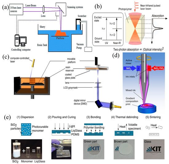
Figure 1. Schemes for (
a) SLA
[39], (
b) TPP, (
c) DLP, (
d) DIW
[14], and (
e) sheet lamination. (
1) (
2) (
3) (
4) and (
5) in (
e) represent each step of the sheet lamination process. (
b) Reprinted with permission from ref.
[40]. (
c) Reprinted with permission from ref.
[41]. (
e) Reprinted with permission from ref.
[33].
2.1. Micro-Stereolithography (μ-SLA)
Micro-stereolithography can be divided into direct laser writing (DLW) technology, which is based on spot exposure, and DLP, which is based on area exposure according to the exposure mode. For DLW, the UV exposure-based technology is usually called stereolithography (SLA), and the femtosecond laser-based technology is called two-photon polymerization (TPP).
2.1.1. Stereolithography (SLA)
SLA, based on photopolymerization, was first patented and commercialized by C. Hull in 1986
[42], and the schematic diagram is shown in
Figure 1a. The first process is to design a 3D model using CAD, then to use a discrete program to slice the model and design the scan path, using the CNC (computer numerical control) equipment to control the laser movement
[24][43][44][45][24,43,44,45]. When the object is processed, the laser spot selectively cures the “liquid glass” photopolymerizable material, accumulating the stack layer by layer until the final 3D object is completed. Because the process uses computerized 3D drawing software to design the internal and external geometry of the structure to be printed, it could be freed from the constraints of traditional molds and be used for the molding and fabrication of many complex components.
SLA was initially used in the additive manufacturing of polymer materials
[42]. With the development of more advanced technology, E. Fantino et al. also applied SLA technology to the additive manufacturing of ceramic and glass materials
[46][47][48][49][50][46,47,48,49,50]. The resolution of SLA depends on the size of the laser spot and generally reaches the tens of microns, which is still far from the standard of micro-optical devices. For this case, the TPP process has been developed.
2.1.2. Two-Photon Polymerization (TPP)
By replacing the UV laser in SLA with a femtosecond laser, TPP could be achieved. TPP is a micro- and nanofabrication technique proposed by Maruo et al. in 1997
[51]. The schematic diagram for TPP is illustrated in
Figure 1b. In this process, a photopolymer absorbs two near-infrared photons simultaneously in a single quantum event whose collective energy corresponds to the UV region of the spectrum. The rate of two-photon absorption is proportional to the square of the light intensity so that the near-infrared light is strongly absorbed only at the focal point within the photopolymer. The quadratic intensity dependence of two-photon absorption allows for the confinement of the solidification to submicron dimensions, which are beyond the diffraction limit of light
[40]. Two-photon polymerization is capable of fabricating 3D micro- and nanostructures at a higher resolution than other processes. Moreover, the lateral resolution of TPP below 100 nm has been demonstrated
[2][52][53][54][55][2,52,53,54,55]. Currently, the use of TPP technology for the additive manufacturing of glass materials is a new trend
[56][57][56,57].
The common problem with DLW technology is the low processing efficiency caused by spot exposure, which usually means it takes hours or even days to process millimeter-level objects using SLA or TPP. Under these circumstances, DLP with the improved light source emerged
[58][59][58,59].
2.1.3. Digital Light Processing (DLP)
DLP technology using an area exposure dates back to 1996, when it initially used liquid crystal displays (LCD) as dynamic displays, though these were replaced in 2001 by digital micromirror devices (DMD). A DMD is a chip that consists of rectangular arrays of hundreds of thousands of micromirrors corresponding to the pixels on the image plane to be displayed
[60][61][62][63][60,61,62,63]. The ultra-fast light switching and integral projection greatly reduce the time required for 3D printing and allow for feature resolutions of a few microns.
Limited by the size of the DMD, with DLP, it is difficult to achieve uniform projection on large surfaces, so the technology is mostly used for the processing of microstructures. Due to the demand for high manufacturing precision and the increase in machinable materials, DLP is considered to be one of the most powerful and versatile processes, and is more suitable for the preparation of micro-optical devices
[64][65][64,65].
Figure 1c demonstrates the schematic diagram for DLP. The devices can be divided into two types according to their structures: bottom-up (left) and top-down (right) systems. The bottom-up system does not break due to gravity and the release force (the pulling force on the inverted equipment when the sample comes out of the bottom of the resin tank), which makes it suitable for massive production, but it is more likely to generate air bubbles and affect the quality of the molded parts. Although the inverted processing technique is affected by gravity and the release force, this processing system has a closed optical path and is relatively safe. The resin flows naturally at the bottom of the resin tank without the influence of air bubbles or uneven liquid levels
[41][66][41,66]. The height of printing is not affected by the depth of the resin, so it can print larger objects with a handful of materials, which makes it more suitable for laboratory design and development.
DLP has received widespread attention because of its printing speed and its ability to achieve micron-level molding precision. In 2017, Frederik Kotz et al. were able to achieve the 3D printing of glass parts by adding SiO
2 nanopowder to the photocuring resin in combination with heat treatment, which also sets a precedent in the field of glass devices using DLP
[35].
In the 3D printing of glass, the three technologies (SLA, DLP, and TPP) of micro-stereolithography (μ-SLA) have something in common. The 3D printing of glass is achieved by adding silica nanoparticles to the polymerization of monomers. The SiO
2 nanoparticles are well dispersed in the polymer monomer and then become suspended with the aid of the necessary surfactants and additives. During the process of 3D printing, the SiO
2 nanoparticles are uniformly surrounded by the cross-linked organic network before being polymerized, forming each layer into a pre-designed shape until the entire structure is built up
[2]. In order to form silica glasses with high density, the printed structure must be processed with suitable heat treatment. The heat treatment process is usually divided into two steps: low-temperature debinding and high-temperature sintering.
2.2. Direct Ink Writing (DIW)
The above-mentioned processes are suitable for the preparation of single-material objects but cannot realize the preparation of multi-material structures. Therefore, the DIW printing process has been developed. DIW is a technique for manufacturing objects by extruding material from a nozzle and depositing it on a selected area. The core components of the technology are the ink material ratios as well as the deposition nozzles, and the technology was first proposed by Cesarano in 1997
[2]. Direct ink writing (DIW) is an extrusion-based additive manufacturing method, which has found a large number of applications in the field of material and tissue engineering. In the process of DIW printing, liquid-phase “ink” is dispensed out of nozzles under controlled flow rates, and then deposited layer by layer along pre-designed paths until the 3D object is fully fabricated
[67][68][67,68]. The sprayed ink is rapidly cured due to evaporative phase change, or gelation, as shown in
Figure 1d.
The process of DIW is relatively simple, allows for inexpensive manufacture, and could be used with a wide range of materials, making it suitable for desktop-level printing. It is also possible to manufacture objects consisting of multiple materials by switching the nozzle
[69][70][71][72][73][69,70,71,72,73]. Furthermore, DIW technology has also been successfully applied by Dylla-Spears’ team to the manufacture of transparent silica glass
[15][74][15,74].
Using DIW technology for 3D printing glass also requires the addition of a suitable amount of silica nanoparticles to the ink of DIW, while the shaping and heat-treatment process is also needed. The difference with the μ-SLA process for printing glass is that the heat treatment parameters need to be altered somewhat due to the different forming methods of the DIW technology.
2.3. Sheet Lamination (SL)
Sheet lamination is also based on the use of “liquid glass” as well as photocuring, and is a technique for replicating structures that uses a soft mold made of PDMS
[33][75][33,75]. This technology allows for the use of “liquid glass” with a higher SiO
2 content because it does not need to take the severe diffuse reflections that occur during SLA/DLP printing into account. In SL, the photocured object is transformed into dense, high-quality glass through heat treatment. The technique is highly efficient, and can accurately replicate objects ranging from the microscale to the centimeter scale. Since the preparation process does not require hazardous chemicals or cleanroom facilities, the manufacturing process is cost-effective and could be performed in any laboratory
[33]. The scheme for sheet lamination is shown in
Figure 1e.
The process of 3D printing glass using the SL process is pretty much the same as with μ-SLA, with the main difference being that SL-printed objects are usually larger in size and require more suitable heat treatment parameters.
3. Applications of 3D Printing Glass Technologies
In the actual processing of 3D glass materials, different forming methods give the forming structure different characteristics. For example, DLW technology is widely used in the laboratory; DIW technology makes it easier to achieve material ratio changing and realize multi-material structure processing; sheet lamination facilitates rolling lamination, so it is suitable for preparing large-sized structures. The unique advantages of these technologies have led to the different applications of 3D printing glass technology.
3.1. Applications of SLA Technology for Printing Glass
The creation of glass devices using the SLA technique is achieved by uniformly dispersing fumed silica nanopowder with a particle size of about 40 nm in a polymer monomer for photocuring, followed by heat treatment
[35]. Due to the poor precision and slow processing speed of the SLA technique, the preparation of glass devices using this technique has rarely been reported, and only Liu et al. have used this technique to prepare rare-earth-doped optical glasses, demonstrating some promising applications
[39][76][39,76].
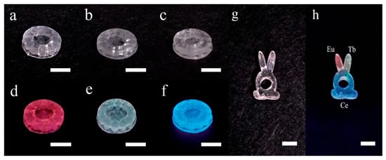
Liu et al. doped glass with rare earth ions (e.g., Eu
3+, Tb
3+, and Ce
3+) using a 3D printing technique, and these emitted red, green, and blue light under the excitation of a 254 nm UV lamp, as shown in
Figure 2a–f. Moreover, the results imply that the shape and function of individual glass devices can be designed through 3D printing. In addition, different rare earth ions were doped at different locations in the glass through selected doping, and Eu
3+ and Tb
3+, as well as Ce
3+, were doped in different areas of a silica glass prepared using the SLA technique. Under natural light, the glass does not show the differences between the regions (
Figure 2g), while under the UV lamp at 254 nm, the different regions can have different fluorescence emissions and realize the colored light emission, as shown in the right of
Figure 2h. The emergence of this technology has turned the realization of different optical properties in the same glass into a reality, which has promoted the development of the field of optoelectronic materials and devices, changed the fabrication of optoelectronic devices, and provided new ideas for the preparation of optoelectronic materials.
Figure 2. Photos of the 3D-printed silica glass doped with (
a) Eu
3+, (
b) Tb
3+, and (
c) Ce
3+ ions, and their luminescent performance under a 254 nm UV lamp are shown in (
d–
f). Photos of selected-area-doped silica glass under (
g) natural light and (
h) 254 nm UV radiation. Scale bar: 5 mm
[75].
3.2. Applications of TPP Technology for Printing Glass
TPP technology could solve the above problems and can directly produce 3D nanostructures whose spatial resolution is well beyond the diffraction limit. In 2021, Thomas Doualle et al. applied two-photon polymerization to 3D-printed glass by adding an appropriate photoinitiator to “liquid glass”, successfully relying on a laser-based process of multi-photon-induced polymerization to produce complex three-dimensional (3D) glass parts
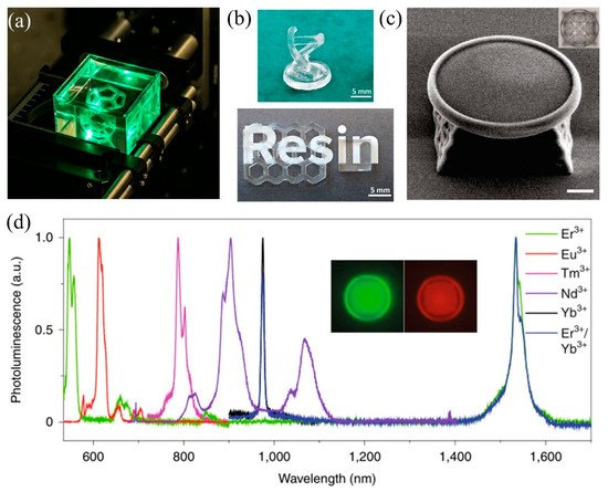
[56]. The object in the process of 3D printing is presented in
Figure 3a, and the successfully printed glass devices are shown in
Figure 3b
[56]. This work pioneered the use of TPP technology for the additive manufacturing of glass materials.
Figure 3. (
a) 3D printing of a complex part in the experimental set-up. (
b) Examples of printed and sintered silica glass parts. (
c) SEM image of the printed micro-toroid optical resonator (scale bar, 10 μm); inset: optical image from the top. (
d) Photoluminescence of Er
3+-, Eu
3+-, Tm
3+-, Nd
3+-, and Yb
3+-doped and Er
3+/Yb
3+ (1:1)-co-doped silica crystal in the visible to near-infrared range; inset: the Er
3+-doped micro-toroid optical resonator under 495 nm (left) and 592 nm (right) excitation and observed at 519 nm (left) and 614 nm (right) using a fluorescence microscope. (
a,
b) Reprinted with permission from ref.
[56] © The Optical Society. (
c,
d) Reprinted with permission from ref.
[57].
Moreover, Wen Xiewen et al. have developed a TPP 3D printing technique using PEG-functionalized colloidal silica NPs that can be highly loaded
[57]. Using 3D printing and post-sintering techniques, high-quality 3D silica structures with arbitrary shapes of amorphous glass or polycrystalline square quartz shapes could be created at resolutions below 200 nm.
Figure 3c illustrates the SEM image of the printed micro-toroid optical resonator.
Figure 3d shows that each photoluminescence peak matches the atomic transition line of a single rare-earth element, confirming the flexibility of the method in the doping/co-doping of rare-earth elements and revealing the potential of constructing passive and active integrated micro-photonic chips using 3D printing.
3.3. Applications of DLP Technology for Printing Glass
DLP printing technology has a faster printing speed compared to SLA and TPP technology and shows great advantages when printing larger-sized objects, and has become a widely chosen and efficient additive manufacturing method in laboratories
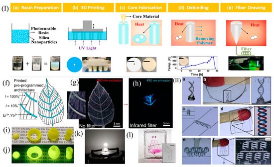
[77][78][79][77,78,79]. The existing literature reports that this technique is mostly used for the preparation of glass devices, including optical fibers, optical glasses, etc., and could also be combined with lamination processes to produce hollow microfluidic channels.
YuShi Chu et al. were the first to use the DLP process to easily prepare the core and cladding of optical fibers by controlling the size and uniformity of silica nanoparticles, and successfully drew the fibers
[34]. The processing procedure of the printing method used for step refractive index fibers is illustrated in
Figure 4I(a–e). The advantage of using DLP photocuring technology is that different refractive indices of the cladding and core can be easily achieved by changing the raw material ratio to ensure light propagation. After the raw materials for the fiber cores are rationed, they are poured into the printed preforms and undergo further thermal curing, as shown in
Figure 4I(c). The prepared preforms were subsequently thermally degreased to remove polymers and other impurities, as depicted in
Figure 4I(d). After debinding, the preform blanks are inserted into Heraeus F300 quartz tubes for support, and fibers with a length of L = 2.3 km are drawn directly on a commercial drawing tower, as shown in
Figure 4I(e). Related tests have shown that the optical fibers prepared through 3D printing have preliminary optical properties.
Figure 4. (
I) (
a–
e) Fabrication process of the step-index silica optical fiber using 3D printing. The patterns of primary and secondary veins are shown in (
f,
g). The area covered with doped glass under infrared light radiation shows intense blue light, as shown in (
h). (
i) Examples of printed and sintered YAG:Ce-PiSG (scale bar, 1 cm) and (
j) the same objects under UV radiation
[16]. (
k) Lighted WLED device in the darkness
[16]. (
l) Microlithography of an exemplary microfluidic chip (inset scale bar, 200 μm) (
II). (
a) Polymeric DNA double helix (scale: 500 μm). (
b) Inverse structure in fused silica glass (scale: 400 μm). (
c) Intertwined spirals (scale: 900 μm). (
d) Resulting intertwined microfluidic spiral channels in fused silica glass with a channel width of 74 μm. The channels were filled with dyes (see inset, scale: 140 μm). (
e) Polymeric microstructures of an out-of-plane mixer structure (scale: 600 μm). (
f) Microfluidic mixer structure in fused silica glass with a channel width of 74 μm (scale bar: 280 μm)
[80][81]. (
I) (
a–
e) Reprinted with permission from ref.
[34] © The Optical Society. (
f–
h) Reprinted with permission from ref.
[81][80]. (
l) Reprinted with permission from ref.
[35].
The technology of 3D-printed glass has great value in optoelectronics as well. David G. Moore et al.
[81][80] realized the 3D printing of glass leaves by regulating the light intensity to verify the accuracy of DLP technology. The rare-earth metals, Er
3+ and Yb
3+, were also directionally doped during the printing process, and the resulting 3D objects were subsequently heat-treated to form silica glass. The final glass leaf has a unique appearance when illuminated with a collimated beam of 980 nm infrared light. Photon up-conversion at the lanthanide-containing voxels turns the incident infrared radiation into blue light, making the primary veins of the glass leaf stand out colorfully in the otherwise transparent and translucent background pattern. The whole process is illustrated in
Figure 4I(f–h). Compared with the previously mentioned SLA technique for preparing rare-earth-doped phosphors, the DLP technique makes it easier to achieve light intensity tuning and enables the more precise realization of locally controllable optical properties.
Moreover, Dao Zhang et al. used modern 3D printing technology to fabricate YAG:Ce-PiSG devices for white light illumination by combining the fabrication process of YAG:Ce-PISG
[16]. The application and performance characterization of white LEDs with laser illumination was also performed, achieving >90% internal quantum efficiency and demonstrating device application, making the free-form manufacturing of fully inorganic color converters a reality and facilitating product design and small volume production, as labeled in
Figure 4I(i–k).
The DLP process has also been greatly applied in the field of microfluidics, and
Figure 4I(l) shows a microfluidic glass chip constructed through microlithography, which initially highlights the application of the process in the field of microfluidics
[35]. The applications can go much further by selecting the suitable material and using DLP technology for stencil structures or immiscible phases, and combing the object with lamination technology to emboss the stencil into the glass structure. Through dissolution, etching, or combustion, which involve the continuous removal of the sacrificial template, and then through the heat treatment process of degreasing, sintering can finally achieve the preparation of complex three-dimensional microstructures in the glass
[82][83][84][85][82,83,84,85]. For example, in 2019, Frederik Kotz et al. proposed applying the sacrificial template method to prepare hollow microstructures in silica glass. PEGDA was used as a template, and various shapes of microfluidic channels have been prepared. All the microfluidic channels are presented in
Figure 4II(a–f). Using this method, microfluidic channel structures with low aspect ratios and high aspect ratios could be easily fabricated, and the prepared 3D structure channels could be reproduced with high fidelity and without distortion
[80][81].
The application of the DLP process to the preparation of optical fibers and microfluidic channels simplifies the preparation process and enables the application of 3D printing in the field of optics and microfluidic channels
[86][87][88][89][86,87,88,89]. DLP has been widely applied and reported, and its advantages are outstanding, although the disadvantage that the preparation of multi-material structures is not able to be realized in one step is still obvious.
3.4. Applications of DIW Technology for Printing Glass
One of the major advantages of DIW is the ability to change the material of the ink easily according to the requirements. For example, Joel F et al. used sol-gel-derived inks to prepare homogeneous, optical quality silica and silica-titanium dioxide glass monoliths through DIW
[74].
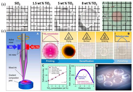
Figure 5a presents glasses prepared using DIW, with the use of the inks obtained through the sol-gel method, and this glass has core-shell TiO
2-SiO
2 nanoparticles with different titanium percentages for glass refractive index tuning.
Figure 5. (
a) Related glass sample with a typical polish, which is fully dense and prepared through DIW. (
b) Two nozzles containing gold and non-gold silica ink were used to print the core-shell structure. (
c) Process and samples of additive manufacturing of gradient index (GRIN) silica-titania glass via DIW
[14]. (
a) Reprinted with permission from ref.
[74]. (
b) Reprinted with permission from ref.
[13].
Another advantage of DIW is that the slurry nozzles can be modified directionally when needed, for example, by adding a second dispensing nozzle to the mechanical bench where multiple materials could be combined. Using this method, a core-shell structure of silicon oxide and silica ink mixed with gold nanoparticles can be formed, as illustrated in
Figure 5b, where the apparent red color is resulted from the surface plasmon resonance of gold nanoparticles at 528 nm due to their strong absorption
[13].
In addition, multi-material blanks containing silica nanoparticles and different concentrations of titanium dioxide as the refractive index modulating dopants were prepared at the Lawrence Livermore National Laboratory. The sample fabrication process using the DIW technique is depicted in A in
Figure 5c
[14]. The optical glasses with different sizes, shapes, and functions in D in
Figure 5c were obtained using the heat treatment process presented in B in
Figure 5c. C in
Figure 5c illustrates the refractive index spatial distribution of the glasses. This shows that the method can be used to achieve a variety of conventional and unconventional optical functions in flat glass components without surface curvature. It is promising to expand the capabilities of 3D printing technology and open the door to the preparation of previously undiscovered functional materials in glass, which may have applications in optics, sensing, packaging, and microfluidic systems.
DIW technology provides a broad idea for the preparation of plasma-resonant multi-component and multifunctional glasses, and the ability to easily adjust the material ratios also highlights the application potential for the preparation of multi-component, multifunctional objects.
3.5. Applications of SL Technology for Printing Glass
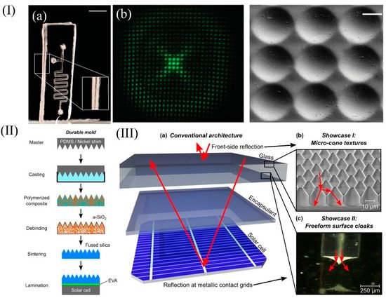
Although the technologies of DLP and DIW are mature enough, the objects fabricated through DLP have an obvious “step effect”, while in DIW, it is difficult to complete the preparation of microstructures. These disadvantages seriously hinder their applications. Sheet lamination can solve these problems well.
The sheet lamination technique, also known as soft replication, usually uses PDMS as a template to obtain the target structure with a reverse mold, and then heat treatment is adopted to obtain the glass microstructure
[31][33][31,33]. For example, the unique process has applications in the field of microfluidic chips, such as the microfluidic glass chip illustrated in
Figure 6I(a), which consists of a two-layer structure that can be easily obtained. Smooth hollow channels are also obtained. In addition to this, the micro-lens array prepared using the sheet lamination technique demonstrates good integrity, which is illustrated in
Figure 6I(b)
[33].
Figure 6. (
I) (
a) A microfluidic glass chip made using sheet lamination (scale bar: 4 mm). (
b) Optical projection pattern obtained from a replicated micro-optical lens array made using sheet lamination with SEM image (scale bar: 15μm). (
II) The processes of the sheet lamination. (
III) (
a) Schematic of the c-Si solar module architecture. (
b) SEM image of the front-side reflection obtained by texturing the front cover glass and (
c) reflection of metallic front contacts obtained by embedding free-form surface (FFS) cloaks into the front cover glass. (
I) Reprinted with permission from ref.
[33]. (
II,
III) Reprinted with permission from ref.
[90].
Malte Langenhorst et al. applied the lamination technology to photovoltaics, applying the optical concept to the conventional architecture of encapsulated solar modules
[90]. The flow chart is labeled in
Figure 6(II), which is also a common process for lamination technology and, subsequently, it is only necessary to prepare the template according to the requirements and optimize the ratio and heat treatment process. The adoption of lamination technology marks the next milestone in the development of FFS cloaks that are compatible with the conventional solar module architecture outlined in
Figure 6III(a). This technology enables the embedding of FFS cloaks into fused silica glass slides, creating a functionalized front cover glass for solar modules. The front cover glass with an embedded FFS cloak fabricated using sheet lamination technology will greatly improve its robustness and durability.
Figure 6III(b) shows an SEM image of the front cover glass, and a close-up view of the air voids due to the embedded FFS cloak is presented in the microscopic image in
Figure 6III(c). This image shows the excellent quality of the liquid glass technique by which FFS can be transferred into fused silica glass. The combination of “liquid glass” and sheet lamination technology to prepare the fused silica front cover glass reduced the frontal reflection loss by 80% and achieved an invisibility efficiency of 88%. Moreover, due to the presence of microstructures, the whole structure has a strong hydrophilic behavior, which may eventually be applied for self-cleaning purposes
[91][92][93][91,92,93].
Using lamination technology, fused silica glass could be processed similarly to a polymer. This method combines the advantages of polymer processing with the excellent material properties of fused silica glass to form a new glass manufacturing method that is more efficient compared to traditional glass processing. The use of sheet lamination fills in the gaps between the manufacturing of micro and large glass components and will enable a wide variety of applications in science, industry, and daily life.
In order to help the readers select more suitable printing technologies and printing materials for glass 3D printing, a summary of the possible printing technologies and materials for 3D printing glass is given in
Table 2.
Table 2.
Some possible technologies and materials for 3D printing glass.
| Technology |
Polymerization of Monomer |
Dispersant |
Photoinitiator |
Stabilizer |
Absorber |
SiO2 |
References |
| SLA |
29.5 wt%HEMA 1+
3.7 wt% PEGDA 2 |
— |
0.4 wt%
DMPA 3 |
13.1 wt% DEDB 4+
0.4wt%MEHQ 5 |
0.3 wt%
Tinuvin 1130 |
53.7 wt% Aerosil OX50 |
[39] |
| |
28.1 wt%HEMA+3.7 wt% PEGDA |
— |
0.4 wt%
DMPA |
14.5 wt%
DEDB |
0.02 wt%
Sudan red G |
53.7 wt% Aerosil OX50 |
[76] |
| DLP |
36.9 wt%HEMA+
6.36 wt% TEGDA 6 |
19.0 wt%
POE 7 |
0.2 wt%
DPO 8 |
0.1 wt %
hydroquinone |
— |
37.5wt% Aerosil OX50 |
[34] |
| |
60 vol%HEMA+
10 vol%TEGDA |
30 vol%
POE |
0.2 wt%
Omnirad 819 9 |
0.1 wt%
hydroquinone |
0.05 wt%
Sudan Orange G |
37.5 vol% Aerosil OX50 |
[35] |
| |
65 vol%HEMA+
35 vol% TMPTA 10 |
— |
0.5 wt%
Omnirad 819 |
0.5 wt%
hydroquinone |
0.45 wt% Tinuvin 384-2 |
35 vol% Aerosil OX50 |
[35] |
| TPP |
80 wt%HEMA |
20 wt%
POE |
1 wt%
BDK 11 |
— |
— |
50 wt% Aerosil OX50 |
[56] |
| |
333 mg ETPTA 12+
666 mgPEGDA |
— |
10 mg
EMK 13 |
5mg
hydroquinone |
— |
1600 mg colloidal silica solution |
[57] |
| DIW |
79 wt%Tetraglyme |
— |
— |
1wt% PDMS |
— |
21 wt%CAB-O-SIL EH-5 |
[13] |
| |
76 wt%Tetraglyme |
— |
— |
1wt% PDMS |
— |
23 wt%CAB-O-SIL EH-5 |
[13] |
| SL |
68 vol%HEMA+
7 vol%TEGDA |
25 vol%
POE |
0.5 wt%
DMPA |
— |
— |
40 vol% Aerosil OX50 |
[33] |
| |
68 vol%HEMA+
7 vol%TEGDA |
25 vol%
POE |
0.5 wt%
DMPA |
— |
— |
50 vol%
silica nanopowder (Zandosil) |
[90] |