Your browser does not fully support modern features. Please upgrade for a smoother experience.
Please note this is a comparison between Version 1 by Sung-Tae Kim and Version 2 by Bruce Ren.
Near-infrared (NIR) photodetectors have interesting roles in optical fiber communications and biomedical applications. Conventional NIR photodetectors have been realized using InGaAs and Ge, of which the cut-off wavelengths exceed 1500 nm. Si-based photodetectors exhibit limited external quantum efficiency at wavelengths longer than 1000 nm.
- CuInSe2
- photodetector
- near infrared
- bandgap energy
- cut-off wavelength
1. Introduction
Nowadays, near-infrared (NIR) photodetectors which can convert optical signals to electrical signals are getting considerable interest for night-vision imaging, optical fiber communications, biomedical imaging, vegetation monitoring, and security applications due to the strong propagation and low attenuation characteristics of NIR light [1][2][3][4][5][6][1,2,3,4,5,6]. Conventionally, InGaAs and Ge-based photodetectors with cut-off wavelengths exceeding 1500 nm have been used for NIR photodetectors. Si-based photodetectors are challenging when used to detect the NIR wavelength range and show low external quantum efficiency due to their low cut-off wavelength of 1100 nm [7][8][7,8]. However, Ge-based photodetectors suffer from a high dark current (~10 mA/cm2) that is orders of magnitude higher than the ~0.5 μA/cm2 of InGaAs photodetectors. This leads to low signal-to-noise ratio (S/N) and responsivity [9][10][11][9,10,11]. InGaAs-based photodetectors have issues related to expensive manufacturing processes [12][13][12,13]. Recently, Cu(In, Ga)Se2 (CIGS) thin films have become considered one of the most prominent candidates for NIR photoactive layers [14][15][16][14,15,16].
Polycrystalline copper-indium-gallium-selenide (CIGS) thin films exhibit very promising properties such as competitive stability, a high absorption coefficient of ~105 cm−1 (two orders of magnitude higher than that of Si), and an adjustable direct energy bandgap (1.04–1.67 eV) [17][18][17,18]. CIGS has gained a reputation as a highly efficient thin film solar cell. The CIGS solar cells have reached a power conversion efficiency (PCE) of 23.35% at laboratory scale [19]. The performance improvement in CIGS solar cells has proven the potential utilization of CIGS thin films for NIR photodetectors. The CIGS thin films can be deposited on top of various substrates such as glass, polyimide, stainless steel, and silicon (Si) so that a CIGS thin film can be utilized to realize NIR photodetectors on various material platforms. Because little research has been reported regarding CIGS as photodetectors, more effort is needed to meet the requirement of the cut-off wavelength needed for operating in the NIR region [20][21][22][20,21,22].
2. CuInSe2 Thin Film with Low Bandgap
A CIGS-based photodetector with a wider spectral range extending into the NIR region could be a candidate for an NIR photodetector. For higher sensitivity in the NIR region, a high-quality photodetector operating in the NIR region using low-bandgap CISe thin film must be realized. The bandgap of CIGS (1.04–1.67 eV) is still too high for use in the NIR region. To achieve a bandgap of about 0.95 eV with a cut-off wavelength of 1305 nm, CISe thin films were grown by the full three-stage process with different durations for the second stage. CISe thin films with Cu/In composition ratios of 1.27 to 0.87 were fabricated.
Figure 1 shows top-view SEM images of CISe thin films grown on the Mo/SLG. The surfaces of CISe films with Cu/In ratios of 0.87 to 0.95 exhibit sharp polyhedral-shaped morphology. The well-faceted polyhedral-shaped grains imply that CISe thin film has a chalcopyrite phase. The grain sizes of CISe films increase as the Cu content increases. For the Cu/In ratios of 0.87 and 0.95, the approximate grain sizes were determined to be about 0.59 and 1.26 µm, respectively. In the Cu-rich state, where the Cu/In ratios are 1.27 and 1.11, the grains exhibited particle-like shapes, and their sizes were 0.91 and 1.14 µm, respectively. The particle-like shapes are ascribed to a large amount of Cu-Se compounds.
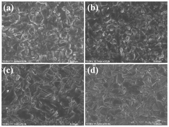
Figure 1. SEM images of CISe thin films with Cu/In ratios of (a) 1.27, (b) 1.11, (c) 0.95, and (d) 0.87.
Figure 2a shows the Raman spectra for the CISe layers. The CISe layers with Cu/In ratios of 1.27 and 1.11 exhibit the A1 mode of the Cu-Se compound, which means an excess amount of Cu. As the Cu/In ratio decreased, the E mode of CISe increased. The highest intensity of A1 mode of CISe (with a Cu/In ratio of 1.27) could be due to the effect of the Cu-Se compound. The XRD patterns in Figure 2b indicate that all of the CISe films have a chalcopyrite crystal structure with a preferred orientation of (112). Even the XRD patterns of all samples did not show an apparent intensity difference. The CISe thin film with Cu/In ratio of 0.95 was expected to have the highest crystallinity from the Raman spectra results.
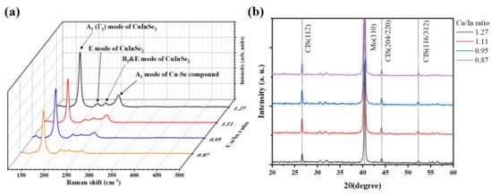
Figure 2. (a) Raman spectra and (b) XRD patterns of the CISe thin films with different Cu/In ratios.
The refractive index (n) and extinction coefficient (k) values were measured using an ellipsometer. The measured n and k values are shown in Figure 3a. The refractive index and extinction coefficient of CISe layers increased as the Cu/In ratio decreased, which suggests that the bandgap of CISe thin film decreased as the Cu/In ratio decreased. The wavelength-dependent absorption coefficients of the CISe layers were extracted from the extinction coefficients. As shown in Figure 3b, the absorption coefficient increased with the decreasing Cu/In ratio.
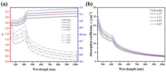
Figure 3. (a) Refractive index, n, extinction coefficient, k, (b) the absorption coefficients of the CISe layers with variable Cu/In ratios.
3. CuInSe2-Based Photodetectors
CISe layers with Cu/In ratios of 0.87, 0.93, 0.94, and 1.02 were utilized to fabricate the photodetectors. The Cu-rich CISe layers, with Cu/In ratios of 1.27 and 1.11, exhibited a Cu-Se compound-related high-defect density on their surfaces, which implies that they are unsuitable for device applications.
The external quantum efficiency (EQE) curves of the CISe thin-film photodetectors with various Cu/In ratios are compared in Figure 4a. The cut-off wavelengths were extracted by extrapolating the EQE curves as shown in the inset of Figure 4a and were utilized to calculate bandgap energies. The bandgap energies of the CISe thin films were tuned by varying the Cu/In ratio from 0.87 to 1.02. As the Cu/In ratio decreased, the bandgap energy decreased, which indicates that an increased cut-off wavelength was realized. The longest cut-off wavelength (1309 nm) was obtained from the CISe thin film having the Cu/In ratio of 0.87. Figure 5b shows the bias current–voltage (I–V) characteristics of the CISe thin-film photodetector in the dark and under 1064 nm laser illumination whose power ranged from 0.83 to 2.33 mW. The CISe-based photodetector with the Cu/In ratio of 0.93 exhibited the dark current density of 28.82 mA/cm2 and the differential resistance of 13.24 kΩ at −0.4 V. The low differential resistance is due to the large shunt leakage current. The dark current and responsivity values of the CISe-based photodetector were compared with those of the previously reported CIGS-based photodetectors in Table 1. Further material growth optimization is required to reduce the dark current and to enhance the differential resistance of the CISe-based photodetectors. In the forward biased condition, the current was almost constant, exhibiting the photovoltaic mode of the device. In the reverse biased condition, the current increased gradually with increasing laser power densities up to 2.33 mW, exhibiting a linear response. This current linear response dependency on the incident optical power is favorable for the photodetectors. The responsivity of the CISe thin-film photodetector was 0.52 and 0.60 A/W at 0 V and −0.4 V, respectively.
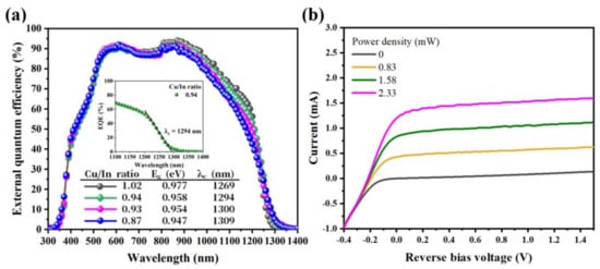
Figure 4. (a) External quantum efficiency (EQE) curves of the CISe photodetectors measured at the bias voltage of −0.4 V. The inset figure shows the method to estimate the cut-off wavelength (λc) from the EQE curve. (b) Current–voltage characteristics of the photodetectors with the Cu/In ratio of 0.93 measured under 1064 nm wavelength.
Table 1. Comparison of dark current values of CIGS and CISe-based photodetectors reported in previous literature.