Your browser does not fully support modern features. Please upgrade for a smoother experience.
Please note this is a comparison between Version 1 by Fei Yi and Version 2 by Dean Liu.
Photodetectors are the essential building blocks of a wide range of optical systems. Typical photodetectors only convert the intensity of light electrical output signals, leaving other electromagnetic parameters, such as the frequencies, phases, and polarization states unresolved.
- metasurface
- photodetector
- multifunctional photodetection
1. Introduction
Silicon PIN photodiode (Figure 1a), based on the internal photoelectric effect, is the most commonly used photon detector, in which the semiconductors absorb the incident photons, and the photo-excited electron-hole pairs in the depletion region are separated by the built-in field and collected by the electrodes. However, the low responsivity in the near-infrared (NIR) spectral band restricts its application in light detection and ranging, as well as optical communication.
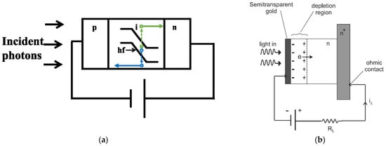
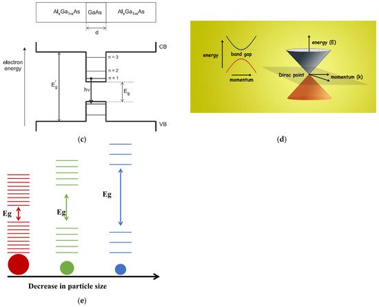
Figure 1. Typical photon detectors: (a) PIN photodiode, (b) Schottky photodiode, (c) quantum well photodetector, (d) graphene photodetector, and (e) colloidal quantum dots photodetector.
Schottky photodiodes (Figure 1b) utilize a metal-semiconductor junction with metal-n − n+ or metal-n configuration to separate and collect the photogenerated charge carriers. Incident photons, with energy greater than the Schottky barrier, pass through a semitransparent metallic layer (often gold) and are absorbed in the depletion region in the n-type semiconductor. Charge carriers generated within the depletion region are efficiently swept out by the built-in electric field, giving rise to a photocurrent. The low responsivity of Schottky photodiodes is due to reflection and absorption of light in the metal layer, as well as poor electron injection efficiency [1][11].
Quantum well infrared photodetector (QWIP) (Figure 1c) is a heterojunction based photodetector, whose energy barrier Eg is determined by the thickness of each layer. However, the intersubband absorption (ISB) in QWIP, at normal incident, is forbidden by polarization selection rule: only the light polarized in the growth direction of the quantum well can cause ISB transitions. Thus, a normal incidence geometry (i.e., light incident normal to the wafer and along the growth direction) is not suitable for photodetection. Thus, various grating structures have been used as the coupler to provide a nonzero polarization component in the epitaxial growth direction [2][12].
Graphene is also an attractive photodetector material due to its zero-bandgap property (Figure 1d), broadband absorption, and ultrafast photoelectric response. However, graphene photodetector suffers from the weak optical absorption of 2.3% [3][13]. This motivates the use of on-chip nanostructures to enhance the light matter interaction in graphene photodetectors.
Colloidal quantum dots (CQDs) (Figure 1e) have emerged as a promising nanomaterial for making low-cost, flexible photodetectors with spectral coverage tunable through the quantum confinement effect using complementary metal-oxide-semi-conductor (CMOS) compatible fabrication process. However, CQD photodetectors face the dilemma of low responsivity, resulting from the much thinner active region than the absorption length. Near-field enhancement, using plasmonic nanostructures, is therefore explored as an effective route to increase the light absorption by scattering.
2. Manipulation of Light by Optical Antennas
Optical antennas are electromagnetic antennas in the optical frequencies. The sizes of optical antennas are usually smaller than the wavelength of light. Thus, optical antennas are subwavelength nanostructures, and the arrays of optical antennas are metasurfaces. Due to the capability of manipulating light at the subwavelength scale, optical antennas and metasurfaces are expected to play significant roles in photodetection by enhancing the light-matter interaction [4][14] and resolving electromagnetic parameters, such as frequencies and polarization states [5][15]. The functions of optical antennas in photodetection can be categorized into three schemes [6][16].- (a)
-
Near field scattering: in this scheme, optical antennas confine the incident light in the vicinity of the nanostructures, enhancing the light-matter interaction and promoting the transduction of photons into electric signals (Figure 2a). Mechanisms for near field scattering include surface plasmon resonance (SPR) and localized surface plasmon resonance (LSPR). SPRs arise from the coupling of electromagnetic fields to the oscillation of the electron plasma in metals, while LSPRs are non-propagating excitations of the conduction electrons in metallic nanostructures coupled to the electromagnetic fields [7][17].
-
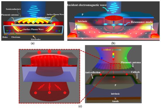 Figure 2. Different functions of optical antennas in photodetection. (a) Near-field scattering, causing locally increased absorption, (b) coupling the incident light into resonant modes and injecting the photo-excited carriers into the semiconductor, and (c) far-field scattering, leading to a prolonged optical path (collect and re-emit photons) [6][16].
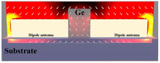 Figure 3. A nanometer-scale germanium photodetector with metal-semiconductor-metal (MSM) configuration is embedded into the gap region of half-wave Hertz dipole antenna. The dipole antenna was used to collect light from a large area and concentrate it into the small subwavelength region of the germanium photodetector [9][19].
-
(b) Resonant detection: in this scheme, the incident light is coupled to the resonant modes in the nanostructured semiconductors and is absorbed efficiently due to the resonantly enhanced light-matter interaction (Figure 2b).
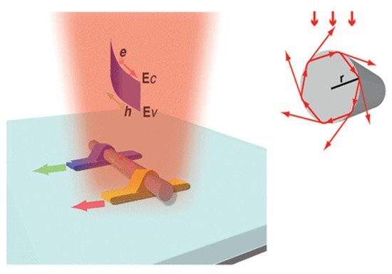 Figure 4. A germanium (Ge) nanowire-based MSM photodetector with asymmetric (one side Ohmic and the other Schottky) metallic contacts.
-
(c) Far field scattering: in this scheme, the metasurfaces (arrays of optical antennas) collect and selectively scatter (or transmit) the incident light into far field, functioning as optical filters, polarizers, or other optical devices (Figure 2c).
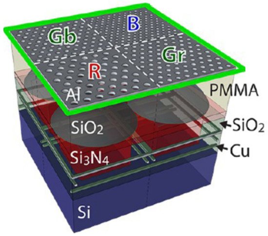 Figure 5. Front-side-illumination CMOS image sensor integrated with RGB plasmonic hole array filters in Bayer mosaic layout.
 -