Your browser does not fully support modern features. Please upgrade for a smoother experience.
Please note this is a comparison between Version 1 by Jie Jian and Version 2 by Rita Xu.
Multilayer films with high-density layer interfaces have been studied widely because of the unique mechanical and functional properties. Magnetron sputtering is widely chosen to fabricate multilayer films because of the convenience in controlling the microstructure.
- multilayer films
- magnetron sputtering
- microstructure evolution
1. Introduction
Due to their unique structures with high-density interfaces, multilayer films have many advanced properties. For example, they are able to maintain high mechanical stability in extreme environments, such as severe tribological conditions with high temperatures [1] and energetic particle irradiation [2][3][4][2,3,4]. W. L. Chen et al. described the high hardness and low friction coefficient of CrAlN/TiAlSiN multilayer films [1]. E. G. Fu et al. demonstrated that Cu/V interfaces effectively reduced the concentration of radiation-induced point defects [5]. In addition, multilayer films have been widely studied for various functional applications, such as hydrogen fuel cells [6][7][6,7] and magnetic data storage [8][9][8,9]. P. Chen et al. posited that Mg/MmM5 multilayer films have good prospects for the application of hydrogen fuel cells because of their synergetic effects [7]. A. M. et al. concluded that multilayer films, such as Co/Pt and Fe/Pt, have beneficial properties for magnetic data storage [9]. This review primarily focuses on multilayer films with metallic systems whose irradiation behaviors are studied extensively.
Among numerous preparation methods, magnetron sputtering provides multiple advantages, including controllable properties, high efficiency, and favorable substrate–film bonding strength; as a result, the benefits of this method are widely exploited in the fabrication of multilayer films [10][11][12][13][10,11,12,13]. For instance, individual layer thickness, one of the most important parameters in determining the properties of multilayer films, can be readily adjusted during the sputtering process [14][15][14,15]. Moreover, this method is also suitable for preparing alloy films and compounds with different compositions [16]. During the sputtering process, multiple parameters play important roles in the microstructure evolution of multilayer films, such as the deposition temperature, rate, bias, and the target–substrate distance. The influences of some parameters have been extensively studied, such as the deposition temperature and bias, whereas other parameters, such as the deposition rate, are not well understood [17][18][19][20][21][22][17,18,19,20,21,22].
Meanwhile, the individual layer thickness also exerts great impacts on the microstructure change of multilayer films, such as the flatness of interfaces, defect density, and coherency [23][24][25][26][23,24,25,26]. When the total thickness of the multilayer films is constant, the thinner the individual layer thickness, the higher the interface density, which may significantly affect many properties of films including the irradiation tolerance. During irradiation, a large population of point defects and larger defect clusters, such as dislocation networks and voids, are introduced into materials under the bombardment of energetic particles [27][28][29][30][31][32][27,28,29,30,31,32]. Such significant microstructure damages can cause swelling, hardening, embrittlement, and other problems in materials which significantly shorten their service life [33][34][33,34]. The irradiation stability of a material can be strengthened through introducing defect sinks, such as grain boundaries (GBs) [35][36][37][38][35,36,37,38], twin boundaries (TBs) [39][40][41][42][43][44][45][39,40,41,42,43,44,45], and free surface [46][47][48][49][50][51][52][46,47,48,49,50,51,52], which facilitate the recombination of irradiation-induced defects and defect clusters. It is well known that interfaces may also act as effective defect sinks [53]. Therefore, multilayer films with high-density layer interfaces are considered as irradiation-resistant materials and have been widely investigated [54][55][56][57][58][59][60][54,55,56,57,58,59,60]. Additionally, multilayer films also have good mechanical properties, such as ductility, yield strength, hardness, etc., which can also be manipulated by changing the parameters during the fabrication process [61][62][61,62].
2. The Effects of Deposition Parameters on the Microstructure of Multilayer Films
2.1. The Effect of Substrate Temperature
In principle, the microstructure and morphology of multilayer films are governed by the kinetics of the mobile adatoms on the substrate, which can be easily controlled by the substrate temperature during the sputtering process [21][63][21,63]. Therefore, the effect of substrate temperature on thin-film fabrication has been widely investigated [2][17][19][64][65][2,17,19,64,65]. During sputter deposition, the mobility of the adatoms, among other factors, drives the condensation, nucleation, and crystallization processes [63]. Higher substrate temperature can provide additional energy for adatoms to migrate and reconstruct into the lowest surface structure, which results in the improvement of the crystallinity, density, etc., of the films [66]. In contrast, the defect density and film roughness decrease [17][21][22][17,21,22]. It is also reported that increasing the substrate temperature can lead to the formation of new compounds between different components of multilayer films, thereby changing the film properties [67].
X-ray diffraction (XRD) patterns of two multilayer systems prepared at different temperatures are shown in Figure 1. Z. Zhou et al. prepared several groups of MgB2/Mo multilayer films at different temperatures. Figure 1a shows that the intensity of the Mo (110) and MgB2 (001) diffraction peaks increases with temperature. Detailed data are listed in Table 1. As the temperature increases from 670 to 730 °C, the Full Width at Half Maximum (FWHM) of the Mo (110) and MgB2 (001) diffraction peaks decreases, indicating the improvement of crystallinity. Additionally, the interplanar spacing of Mo (110) increases with the deposition temperature and eventually reaches 0.2236 nm at 730 ℃ compared to the standard value of 0.2225 nm, indicating that the residual tensile stress of the Mo layers increases with rising temperature due to the reduced defect density in the films [24].
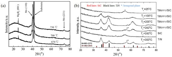
Table 1. The FWHM and interplanar spacing data obtained from the XRD curves of MgB2/Mo multilayer films prepared at different temperatures [24].
| Layer | T/°C | FWMH/(°) | d/nm |
|---|
[67]. This phenomenon can change the irradiation behavior of the films.
In conclusion, manipulating the substrate temperature can change the crystallinity, density, composition, surface roughness, etc. In general, raising the substrate temperature can increase the grain size, improve the crystallinity and density of multilayer films, and reduce defect density and surface roughness. However, high deposition temperature may also lead to the formation of high-density misfit dislocations, thereby reducing the crystallinity and surface flatness. In addition, new compounds may form in some multilayer systems with miscible interfaces and negative heat of mixing when sufficient heat is provided.
2.2. The Effect of Deposition Rate
The deposition rate is not an independent parameter that can be directly controlled in the sputtering process. In general, the deposition rate can be adjusted by manipulating other parameters, such as deposition power (sputtering power), gas pressure, or target–substrate distance [69]. The deposition power, among other parameters, is frequently chosen to adjust the rate [53]. Table 2 shows the FWHM and the signal-to-noise ratio (SNR) of XRD curves of Cu/Nb multilayer films deposited at different substrate temperatures with different deposition rates of Cu. Several selected SEM micrographs are shown in Figure 2d–f. In this case, slower deposition rates could give the adatoms enough time to migrate and arrange according to the normal lattice structure. As a result, the defect density in Cu decreases and also leads to a decreased defect density in the adjacent Nb layers. Consequently, the crystallinity of the multilayer films is promoted [2]. However, decreasing the deposition rate also enhances the probability that Cu atoms will migrate between adjacent layers, which adversely affects the layer continuities, as shown in Figure 2e,f [2].
Table 2. The average FWHM and SNR of the main peaks obtained from XRD curves of Cu/Nb multilayer films deposited at different temperatures and Cu deposition rates [2]. Reprinted with permission from [2] Elsevier 2011.
| Deposition Temperatures | Cu Deposition Rates | ||||||
|---|---|---|---|---|---|---|---|
| 0.5 nm/s | 2.5 nm/s | 5 nm/s | |||||
| FWHM /(°) | SNR | FWHM /(°) | SNR | FWHM /(°) | |||
| Mo (110) | 670 | 0.845 | 0.2229 | ||||
| 700 | 0.743 | 0.2232 | |||||
| 730 | 0.642 | 0.2236 | |||||
| MgB | 2 | (001) | 670 | 0.105 | 0.3531 | ||
| 700 | 0.063 | 0.3530 | |||||
| 730 | 0.044 | 0.3532 | |||||
The grazing incidence X-ray diffraction (GIXRD) patterns of TiN/SiC multilayer films deposited at a series of temperatures are shown in Figure 1b. When the deposition temperatures are 25 and 100 °C, the structure of the multilayer films consists of nanocrystalline TiN layers with small grains and amorphous silicon carbide layers. As the substrate temperature increases to 200 and 350 °C, amorphous SiC begins to crystallize. In comparison, pure SiC films are still highly amorphous at this temperature [68]. Evidently, the crystallinity of the multilayer films can be improved by increasing the temperature. However, a special case exists if the thermal energy can overcome the activation energy of defect proliferation when the deposition temperature exceeds a certain threshold, such as 600 °C for Ge/Si multilayer films. Consequently, high-density misfit dislocations are formed, which jeopardize the crystallinity of multilayer films [19].
Figure 2 shows scanning electron microscope (SEM) micrographs of two multilayer systems. The effect of substrate temperature on the microstructure of the films can be observed. As shown in Figure 2a–c, the surface of WS2/Fe/a-C/Fe multilayer films becomes smoother and denser at higher substrate temperatures. In general, a sputtered Fe layer shows a porous columnar structure; however, when deposition temperature is increased, the adatoms obtain enough energy to fill the channels between columnar grains. As a consequence, the shadow effect caused by Fe layers is mitigated, forming smoother and denser films [22].
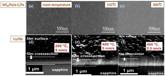
Figure 2. SEM micrographs of (a–c) WS2/Fe/a-C/Fe [22] and (d–f) Cu/Nb [2] multilayer films deposited at different temperatures. The morphology of multilayer films becomes smoother with rising deposition temperature. The cross-sectional images of Cu/Nb show the deterioration of layer continuities with an increasing substrate temperature and decreasing deposition rate. Reprinted with permission from [22] Elsevier 2020, [2] Elsevier 2011.
It is worth noting that higher substrate temperature does not always produce lower film roughness. This conclusion only applies to the temperature at which the aggregation of small grains is suppressed. Otherwise, the film surface will become rougher due to the formation of large grains. T. Wu et al. experimentally demonstrated that the smoothest morphology was obtained when the substrate temperature was ~200 °C for Au/NiCr/Ta multilayer films. Further increasing the temperature caused a rougher film surface [17].
Figure 2d,f present the effect of deposition temperature on the microstructure change of Cu/Nb multilayer films. The morphology of the film surface shows larger grains at higher deposition temperatures. The cross-sections of the films show that the multilayer films deposited at 200 °C have better continuity in their layers than those at 400 °C. This is because the energy of adatoms decreases at a lower temperature and fewer Cu atoms can diffuse to the adjacent Nb layers, resulting in much fewer pinch-off events [2].
Increasing the substrate temperature can also change the composition of multilayer films, such as Ni/Al multilayer films. Previous studies have shown that L12-ordered Ni3Al can be obtained in Ni/Al multilayer films either by post-annealing or by increasing the substrate temperature during fabrication
| SNR | |||||||
|---|---|---|---|---|---|---|---|
| 750 °C | Cu | 0.6 | 1663 | 0.5 | 596 | 0.5 | 588 |
| Nb | 0.8 | 521 | 0.9 | 292 | 0.8 | 1012 | |
| 600 °C | Cu | 0.9 | 1226 | 0.9 | 886 | 0.8 | 488 |
| Nb | 1.1 | 489 | 1.2 | 327 | 1.1 | 224 | |
| 400 °C | Cu | 1.6 | 309 | 1.7 | 256 | 1.4 | 226 |
| Nb | 1.5 | 131 | 1.7 | 122 | 1.7 | 54 | |
| 250 °C | Cu | 1.3 | 211 | 1.3 | 112 | 2.2 | 179 |
| Nb | 1.5 | 106 | 1.6 | 89 | 3.6 | 124 | |
| 200 °C | Cu | 3.4 | 128 | ||||
| Nb | 4.6 | 122 | |||||
| 150 °C | Cu | 5.2 | 116 | ||||
| Nb | 5.8 | 68 |
Many previous studies have reported that the deposition rate can be easily controlled by the deposition power and higher deposition power normally leads to a faster deposition rate. However, it is worth mentioning that high power may also introduce a high degree of ionization, high plasma density, and hence high ion flux towards the substrate, which will eventually affect the microstructure and morphology of the films [70]. Clearly, the effects of the deposition rate on the microstructures of multilayer films need further investigation.
2.3. The Effect of Deposition Bias
The bias voltage is another important parameter in the sputtering process. Increasing the bias will increase the energy of the sputtered particles [20]. As a consequence, the adatoms possess higher energy, affecting the microstructure and morphology of the multilayer films [71]. The XRD curves of CrN/MoN multilayer films deposited at different biases are shown in Figure 3a–c. The results indicate that the texture of the films can be altered by changing the deposition bias. For instance, the films exhibit strong (311) texture when the applied bias Ub = −20 V. As Ub increases to −150 V, solid solution (Cr, Mo) N forms at the interfaces between the layers, resulting in predominantly (111) texture, as shown in Figure 3b. When Ub is further increased to −300 V, the content of N decreases, leading to the preferred formation of the (200) texture [72].
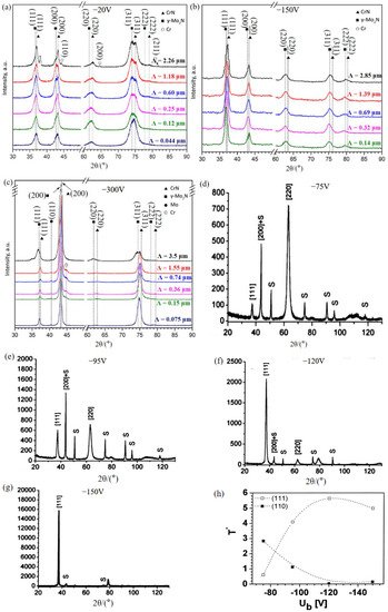
The texture changes of CrAlYN/CrN multilayer films grown on a CrAlN base layer and prepared under different biases are shown in Figure 3d–h and Figure 4a–d. With the increase in bias voltage, the preferred texture gradually evolves from a mixture of (220) and (222) textures to a predominant (111) texture. The texture evolution is summarized in Figure 3h. It is evident that as the bias increases, the intensity of (110) texture gradually declines, while the intensity of the (111) texture is gradually enhanced. When the bias is above −120 V, the films exhibit primarily (111) texture. The texture evolution is mainly attributed to the increased internal stress in the films at a larger bias because the CrAlYN/CrN multilayer films exhibit a face-centered cubic (FCC) structure and the (111) texture is preferred under greater stress [20].
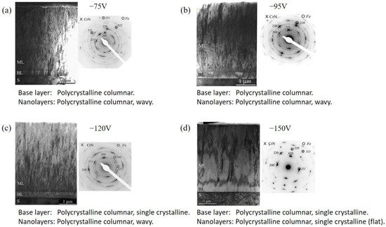
Figure 4. Transmission electron microscope (TEM) micrographs and selected-area electron diffraction (SAED) patterns of CrAlYN/CrN multilayer films deposited at (a) Ub = −75 V, (b) Ub = −95 V, (c) Ub = −120 V, and (d) Ub = −150 V, showing the change in the microstructure of multilayer films with different deposition biases [20]. Reprinted with permission from [20] American Vacuum Society 2009.
The TEM micrographs and corresponding SAED patterns in Figure 4 show the microstructure change of CrAlYN/CrN multilayer systems with different biases. In addition to the change in texture, because the energy of sputtered particles increases with a rise in bias, different microscopic morphologies are formed. When the bias voltage is −75 V, as shown in Figure 4a, both the base layer (CrAlN) and the above multilayers are polycrystalline with columnar grains. When the bias voltage increases to −95 V, the density of the layers increases due to the enhanced energy of the sputtered particles. As can be observed in Figure 4b, the size of the columnar grains and the density both increase. As the base layer contains both columnar and large single-crystal domains with a strongly pronounced local epitaxial growth on the substrate, the base layer forms a single-crystal structure under the bombardment of high-energy adatoms as the bias voltage increases to −120 V, whereas the multilayer structure remains polycrystalline. When the bias voltage increases to −150 V, a single-crystal structure is present in both the base layer and the multilayers [20].
In conclusion, manipulating the bias can change the stress, density, composition, texture orientation, crystallinity, crystal structure, etc. In general, as the bias increases, the stress in the multilayer films rises, thereby improving the crystallinity and density, and the texture is prone to change into the orientation with lower energy. The composition can also be changed with different biases, which will also affect the texture of the films.
2.4. The Effect of Target–Substrate Distance
The target–substrate distance is another parameter that can be manipulated to modify the microstructure of multilayer films in the sputtering process. In general, shortening the target–substrate distance will increase the energy of adatoms, thereby altering the crystallinity, density, and other properties of the multilayer films. Notably, shortening the target–substrate distance can promote the sputtering rate but also decrease the uniformity of the films [73]. Therefore, an appropriate target–substrate distance is important during the film fabrication process.
In many cases, the crystallinity of the films is determined by the energy of the adatoms [67]. Figure 5 shows hydroxyapatite (HA)/Ag multilayer films prepared at different target–substrate distances and temperatures. As is clearly shown in Figure 5a,b, the shorter the target–substrate distance, the sharper the XRD diffraction peak, indicating better crystallinity of the films. When the target–substrate distance decreases from 8 to 4 cm, sputtered particles have a lower probability of colliding and decelerating, and the adatoms retain higher energy, resulting in a higher crystallinity of the multilayer films. Table 3 shows the crystallite size of HA/Ag multilayer films prepared at different substrate temperatures and target–substrate distances. Shorter target–substrate distances result in a higher energy of the adatoms, leading to the formation of larger grains. When the target–substrate distance reaches 8 cm, the amorphous structure can even be produced at room temperature [18].
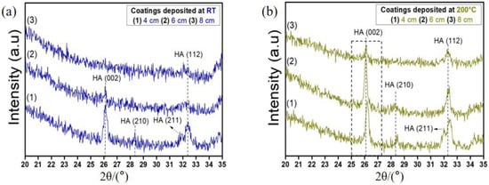
Figure 5. XRD patterns of hydroxyapatite (HA)/Ag multilayer films deposited at (a) room temperature (RT), (b) 200 °C and different target–substrate distances. The crystallinity of multilayer films is enhanced with increasing deposition temperature and decreasing target–substrate distance [18]. Reprinted with permission from [18] Elsevier 2019.
Table 3. The crystallite size of HA/Ag multilayer films prepared at different substrate temperatures and target–substrate distances [18]. Reprinted with permission from [18] Elsevier 2019.
| Sample | Crystallite Size (nm) | |
|---|---|---|
| Coatings Deposited at: | ||
| RT | 200 °C | |
| 4 cm | 26.22 | 29.38 |
| 6 cm | 17.64 | 30.24 |
| 8 cm | Amorphous coating | 19.79 |