Your browser does not fully support modern features. Please upgrade for a smoother experience.
Please note this is a comparison between Version 2 by Jason Zhu and Version 1 by Bin Zhang.
Due to the outstanding physical, chemical, electronic, and optical properties, ultra-thin 2D materials can be potentially utilized in a wide spectrum of applications, including catalysis, energy storage, sensors, biomedicine and electronics/optoelectronics, etc.
- 2D Nanomaterials
- Optical Limiting
- Graphene
- Antimonene
1. Graphene
Graphene and its derivatives have been widely used in the preparation of optical limiting materials due to the ultra-broadband resonate NLO response and the ultrafast carrier relaxation dynamics that are derived from its extended conjugate sp2 π-system and linear dispersion relation of its electronic band structure. Recent advances of graphene-based optical limiting materials have been summarized in a comprehensive review [48][1].
Most recently, Chen et al. innovatively designed and synthesized the chemically modified reduced graphene oxide materials with aggregation-induced emission (AIE) polymer for solid-state optical limiters [49][2]. As shown in Figure 1a, the AIE-active polymer PBFTB was synthesized with Suzuki coupling reaction. By converting the bromine group to azide group, the polymer PAHFTP was functionalized on the surface of reduced graphene oxide via nitrene chemistry. The solid-state PFTP-RGO film showed typical RSA response at both 532 and 1064 nm, indicating it could be the potential broadband OL materials. From Figure 1b, it can be clearly seen that the annealed PFTP-RGO/PMMA film has the lowest normalized transmittance (Tmin) under both 532 and 1064 nm irradiation, indicating the best OL performance. Moreover, Figure 1c showed the OL threshold (the input influence or energy at which the Tmin is 50% of the linear transmittance) and the nonlinear coefficients (βeff) of the samples. Under the laser intensity of 300 μJ, by comparison with RGO/PMMA and PFTP-RGO/PMMA film, the annealed PFTP-RGO/PMMA film obtained the lowest OL thresholds (1.44 J/cm2 at 532 nm and 1.08 J/cm2 at 1064 nm) and the largest nonlinear coefficients (296.79 cm/GW at 532 nm and 369.89 cm/GW at 1064 nm). These values are among the best of the reported graphene-based NLO materials, providing a new avenue for designing ultra-broadband OL materials.
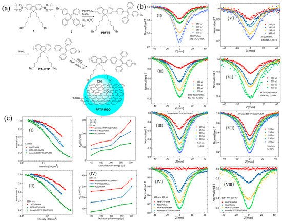
Figure 1. (a) Synthesis of PFTP-RGO; (b) Typical open-aperture Z-scan data for the PMMA-based films excited under 6 ns pulses at 532 nm (I–IV) and 1064 nm (V–VIII), respectively. The solid lines are the theoretical fitting results; (c) Variation of the normalized transmittance as a function of input laser intensity for the films at 532 nm (I) and 1064 nm (II), and the corresponding βeff coefficients as a function of the excitation pulse energy (III, IV). Reprinted with permission from [49][2]. Copyright 2018 WILEY-VCH Verlag GmbH & Co. KGaA, Weinheim.
2. Black Phosphorus
As a rising star among the 2D nanomaterials family, black phosphorus (BP) has been extensively investigated due to its outstanding, high electron/hole mobility, thickness-dependent tunable bandgap, large photon-to-electron quantum yields [85][3], superior thermodynamic stability, and broadband nonlinear optical response. Figure 2a,b shows the non-planar, puckered architecture of BP, which consists of fused hexagons of sp3-hybridized P atoms [86,87,88][4][5][6]. The STEM image shows the aesthetically pleasing lattice structure of BP. However, in the presence of oxygen, BP will rapidly degrade within the scope of hours. This lack of stability under ambient conditions severely undermines the application of BP, which is still a formidable challenge for researchers to conquer.
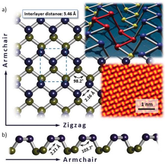
Figure 2. (a) Top view of the puckered honeycomb lattice of black phosphorus (BP). Upper plane P atoms are marked in blue, lower plane P atoms are in yellow; (b) lateral view on the lattice in armchair direction. Characteristic distances and angles according to Castellanos-Gomez et al. [87][5]. Insets: BP lattice with a six-membered ring in chair configuration highlighted in red; scanning tunneling electron microscopy (STEM) image of the BP lattice. Reprinted with permission from [88][6]. Copyright 2018 WILEY-VCH Verlag GmbH & Co. KGaA, Weinheim.
Fan et al. first reported the broadband NLO response in multi-layer BP nanoplatelets both in solution and solid state [89][7]. As shown in Figure 3a, the multi-layer BP nanosheets were obtained by liquid exfoliation from bulk BP crystal. For BP dispersions, characterized by the wide-band open-aperture Z-scan techniques, saturable absorption (SA) was observed under femtosecond at both 400 nm and 800 nm (Figure 3b–d). The achieved saturation intensity and normalized transmittance value were 455.3 ± 55 GW/cm2 and 27.6% at 400 nm, 334.6 ± 43 GW/cm2 and 12.4% at 800 nm. For BP/PMMA thin film, similar results were also observed under picosecond excitations at both 1562 nm and 1930 nm and the corresponding values were 18.54 MW/cm2 and 19.5% at 1563 nm, and 4.56 MW/cm2 and 16.1% at 1930 nm. By centrifuging at 3000 rpm to remove the multi-layer BP, the few-layer BP nanosheet was obtained by centrifuging the supernatant at 12000 rpm (Figure 4a). As shown in Figure 4b, Chu et al. demonstrated that the few-layer BP nanosheet also exhibited the SA behavior in NMP at 800 nm with pulse width of 100 fs [90][8]. By using few-layered BP as an electron donor and C60 as an electron acceptor, Yu et al. successfully prepared the donor–acceptor (D-A) type blends and embedded them in the poly(methylmethacrylate) (PMMA) matrix as a solid-state optical limiter [91][9]. Due to the thermal-induced intermolecular charge transfer effect between BP and C60, the annealed BP:C60/PMMA film showed an enhanced optical limiting response at 532 nm. The nonlinear coefficient, the limiting threshold, and the damage threshold were 241.73 cm/GW, 4.5 J/cm2, and 19.54 J/cm2, respectively (Figure 4c). This creative strategy for designing such novel D-A type blends offers new solutions for constructing the next generation optical limiters.
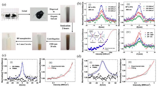
Figure 3. (a) The preparation process of BP nanoplatelets; (b) (I) and (II) are the open aperture Z-scan measurements of BP NPs dispersions under different intensities at 400 nm and 800 nm, respectively; (III) The relation between normalized transmittance and input intensity for BP NPs dispersions at 800 nm; (IV) The open aperture Z-scan measurements of BP NPs dispersions in IPA, NMP, and EA at intensities of 515 GW/cm2; (c) (I) The open aperture Z-scan measurements of BP-PMMA on quartz at peak intensity of 4.1 MW/cm2 and (II) relation between normalized transmittance and intensity at 1563 nm band; (d) (I) The open aperture Z-scan measurement of BP-PMMA on quartz at peak intensity of 0.66 MW/cm2 and (II) relation between normalized transmittance and intensity at 1930 nm band. Reprinted with permission from [89][7]. Copyright 2015 The Optical Society.
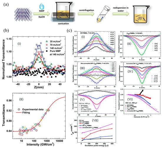
Figure 4. (a) Schematic illustration of the fabrication process of basic-N-methylpyrrolidone(NMP)-exfoliated phosphorene; (b) (I) Open-aperture Z-scan measurements of phosphorene dispersions at 800 nm. (II) The relationship between transmittance of the phosphorene dispersions and intensity of the femtosecond laser; Reprinted with permission from [90][8]. Copyright 2015 WILEY-VCH Verlag GmbH & Co. KGaA, Weinheim. (c) (I–V) Typical open-aperture Z-scan data with normalized transmittance as a function of the sample position Z for the samples embedded in a PMMA matrix under the excitation of 6 ns pulses at λ = 532 with different energies. The solid lines are the theoretical fitting results; (VI) variation in the normalized transmittance as a function of input laser intensity for the PMMA-based films at 532 nm; and (VII) βeff as a function of the excitation pulse energy for these samples. Reprinted with permission from [91][9]. Copyright 2018 Royal Society of Chemistry.
However, for large scale production, it is difficult to control the thickness and lateral size of BP nanosheets by liquid exfoliation. Ultrasmall quantum dots (QDs) are another morphology of 2D materials with a particle size less than the exciton Bohr radius. Due to the existence of the quantum-confinement effect, QDs usually exhibit some excellent physical and chemical properties, especially in the field of optoelectronics. As depicted in Figure 5a, by using the solvothermal method, Yu et al. successfully prepared the black phosphorus quantum dots (BPQDs) with an average size of 2.1 ± 0.9 nm from bulk BP crystal and used it as an optical saturable absorber [92][10]. The achieved saturable intensity and modulation depth were 3.3 GW/cm2 and 36% (Figure 5b). Similar results were also obtained by other researchers and these results demonstrate that BP and its derivatives could be an extraordinary candidate for ultrafast photonics devices. Furthermore, the work of non- and covalent functionalization of BP as OL materials is well worth exploring, especially the covalent functionalization, as it is considered to have better and more stable physicochemical properties than non-covalent modifications.
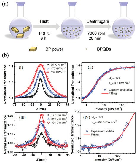
Figure 5. (a) Schematic representation of the synthesis process to prepare black phosphorus quantum dots (BPQDs) by using a solvothermal method in NMP; (b) The experimental results and fittings measured by Z-scan technique at 800 nm. The open Z-scan curves for (I) BPQDs and (III) BP nanosheets. The normalized transmittance and input peak intensity for (II) BPQDs and (IV) BP nanosheets. Reprinted with permission from [92][10]. Copyright 2016 WILEY-VCH Verlag GmbH & Co. KGaA, Weinheim.
3. Antimonene
In contrast to the instability of BP in air, which has greatly limited the application scope of BP and its derivatives, antimonene, the group-VA element composed 2D material, was recently predicted to be of good stability [93][11]. Figure 6illustrates the atomic structure of β-phase antimonene; the monolayer β-phase antimonene consists of buckled hexagonal rings composed of Sb atoms connected through sp3 bonding and the layer distance is about 0.38 nm. According to theoretical calculations, antimonene presents high carrier mobility, superior thermal conductivity, strain-induced band transition and promising spintronic properties [94,95,96,97,98][12][13][14][15][16]. Although the antimonene possesses these excellent properties, reports in the field of nonlinear optical are still scarce. Zhang et al. first reported the NLO response of few-layer antimonene decorated microfiber with the exciting source at 800 and 1500 nm, and the pulse duration is 95 fs and repetition rate is 1 kHz [99][17]. Figure 7b illustrates the evanescent field method of depositing few-layer antimonene nanoflakes onto a piece of microfiber. From Figure 7a, it can be seen that antimonene showed the typical SA response, and the achieved saturable intensity and modulation depth are 14.25 GW/cm2 and 3.96% at 800 nm and 15.10 GW/cm2 and 19.72% at 1500 nm. However, the RSA response of antimonene was observed by Xu et al. for the first time [100][18]. When the pulse energy was above 7.43 μJ excitation at 1064 nm, the competitive process between single photon absorption (1PA) and two-photon absorption (TPA) was observed (Figure 7c). The same phenomenon was also observed at the higher energy of visible region (532 nm), suggesting antimonene could be the TPA-dominant OL materials.
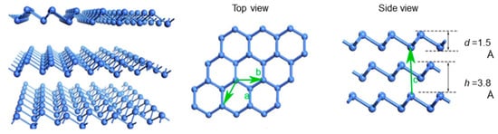
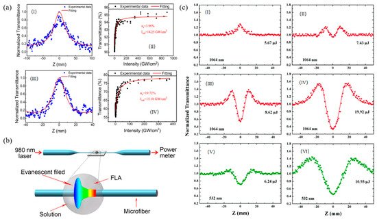
Figure 7. (a) The open-aperture Z-scan measurements of antimonene at 800 nm: (I) measurement of antimonene on quartz and (II) the relation between transmittance and input intensity. Open-aperture Z-scan measurements of antimonene at 1500 nm: (III) measurement of antimonene on quartz and (IV) the relation between transmittance and input intensity; (b) fabrication of FLA decorated microfiber: a schematic diagram of the evanescent field method for trapping antimonene nanoflakes on the sidewall of a microfiber. FLA: few-layer antimonene; Reprinted with permission from [99][17]. Copyright 2017 IOP Publishing Ltd. (c) Open-aperture Z-scan measurement results of antimonene nanosheets upon excitation at (I–IV) 1064 and (V and VI) 532 nm wavelengths with different excitation intensities (the points are the experimental data and the solid lines are the fitted curves). Reprinted with permission from [100][18]. Copyright 2018 Royal Society of Chemistry.
4. Hexagonal Boron Nitride Sheets (h-BN)
Hexagonal boron nitride (h-BN), which is called the “white graphene”, has a similar lattice structure to graphene (Figure 8a) [101][19]. However, in contrast to the zero bandgap of graphene, h-BN has a wide bandgap of about 6.1 eV at room temperature demonstrated by experimental and theoretical studies. Due to the high-temperature stability, outstanding mechanical strength, intrinsic electrical insulation and anti-oxidation capacity [102[20][21][22],103,104], h-BN may have the potential of being a nonlinear optical material. The NLO properties of h-BN dispersion were first studied by Ajayan et al. and the typical OL response was observed at 1064 nm with the pulse duration of 10 ns [105][23]. The tested data fitted well with the TPA and the largest achieved TPA coefficient was 74.84 cm/GW at the peak intensity of 0.02 GW/cm (Figure 8b). From a practical application point of view, it is better to fabricate solid-state optical limiters by embedding the NLO materials as inclusions in a suitable non-optically active host and/or polymerizing the NLO chromophore-based monomers to form composite functional materials [49][2]. Hao et al. investigated the NLO response of h-BN nanosheets (BNNSs) in both solution and solid state [106][24]. The MTES hybrid gel glasses of BNNSs were successfully prepared by the modified molten hydroxide exfoliation method and the Z-scan test was performed at 532, 1064, and 2000 nm (Figure 8a). By comparison with carbon nanomaterials (i.e., graphene and graphene oxide), the BNNSs showed superior OL performance both in solution and solid state which can be explained by the good transparency, high thermal conductivity, and stability of BNNSs. Meanwhile, due to the long-term optical, thermal, and mechanical stability of the ormosil glasses, the MTES hybrid gel glasses of BNNSs have a better performance than BNNSs dispersion. The ultra-broadband NLO response of h-BN, ranging from 500 to 2000 nm, were deduced from the combination of NLA, NLS, and NLR, indicating h-BN could be another promising OL material after graphene.
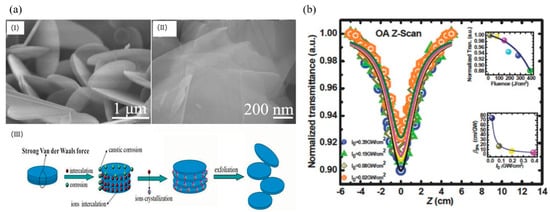
Figure 8. (a) SEM images of raw materials (I) and folded hexagonal boron nitride (h-BN) nanosheets (II), (III) Schematic illustration of the “chemical weathering” exfoliation of hexagonal boron nitride; Reprinted with permission from [101][19]. Copyright 2015 WILEY-VCH Verlag GmbH & Co. KGaA, Weinheim. (b) Depicts the intensity-dependent OA Z-scan transmission trace of the aqueous dispersion of h-BN nanosheets (BNNSs). Symbols are experimental points and solid lines are theoretically obtained considering 2PA in the sample. Inset (top) shows the optical limiting effect and the inset (bottom) shows the intensity-dependent variation of β2PA showing saturation of 2PA. Reprinted with permission from [105][23]. Copyright 2015 WILEY-VCH Verlag GmbH & Co. KGaA, Weinheim.
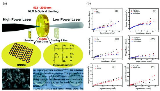
Figure 9. (a) Schematic of nonlinear optical (NLO) and optical limiting (OL) functional BNNSs with hybrid ormosil gel glass, coating, and film; (b) OL responses of ethanol solutions and methyltriethoxysilane(MTES) hybrid gel glasses of BNNSs and graphene derivatives. Ethanol solutions at 532 (I), 1064 (III), and 2000 nm (V) with 75% linear transmission. MTES hybrid gel glasses at 532 (II), 1064 (IV), and 2000 nm (VI) with the same doping concentration of 0.1 wt%. Reprinted with permission from [106][24]. Copyright 2018 Royal Society of Chemistry.
5. Transition Metal Dichalcogenides (TMDs)
Transition Metal Dichalcogenides (TMDs), of which the general formula is MX2 (M=Mo, W, Nb, Ta; X = S, Se), is analogous to graphene and has a layered structure [27][25]. The TMD monolayer structure contains three atomic layers and the middle layer is the transition metal layer. The layered TMDs crystals are stacked by the van der Waals force and the most characteristic feature of TMDs is their capability to form different crystal polytypes. MoS2, as the prototypical TMD, has five different crystal structures, naming 1H, 1T, 1T′, 2H, and 3R (Figure 10a). Due to the different crystal polytypes, ultrafast carrier dynamics, and ultrafast nonlinear absorption, much attention has been focused on the study of nonlinear optical properties of TMDs. Wang et al. systematically investigated the NLO behavior of MoS2, MoSe2, WS2, WSe2, and graphene nanosheets with the excitation wavelength of 532 and 1064 nm [107][26]. Both TMDs and graphene strong optical limiting responses at 1064 nm, which originated from the NLS (Figure 10b). However, at 532 nm, the TMDs showed a combination of SA and NLS response. Among these materials, the performance of the selenium compounds is superior to the sulfide compounds in the near infrared region. However, little work has focused on the impact of different crystal structure on the electronic and optical properties. As the most stable phase at ambient conditions, the 2H phase TMDs have been widely used in transistor devices. While the less stable 1T’ phase exhibits some unique properties, such as dipolar ferroelectricity, Weyl semimetal, and quantum spin Hall effect, et al. [108,109,110,111][27][28][29][30].
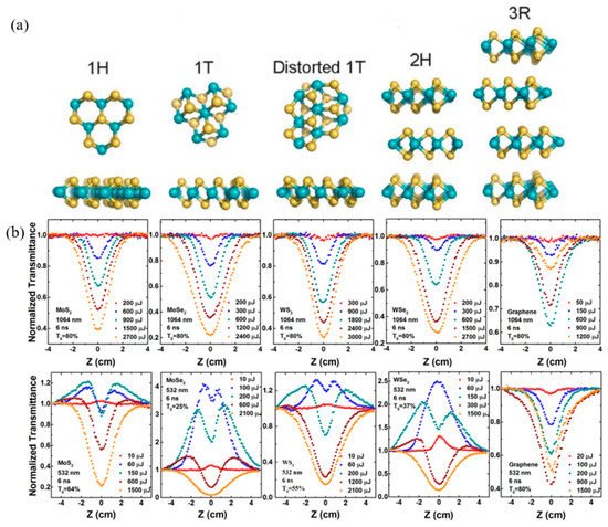
Figure 10. (a) Crystal structures of MoS2 with different polymorphisms. Reprinted with permission from [27][25]. Copyright 2017 American Chemical Society. (b) Typical open-aperture Z-scan data with normalized transmittance as a function of the sample position Z for the MoS2, MoSe2, WS2, WSe2, and graphene dispersions in NMP at 1064 and 532 nm, respectively, with different incident laser pulse energy. Reprinted with permission from [107][26]. Copyright 2015 Springer Nature Limited.
By intercalating the alkali metal hydrides, which served as the electron donors, the complete phase conversion from 2H-to-1T′ took place and the 1T′ phase of MoS2 and WS2 showed unprecedented long-term stability in the ambient environment [112][31]. Under the excitation of a femtosecond laser at 900 nm, the 1T′ phase few-layered h-LiMoS2 exhibited the typical SA response, while the 2H phase MoS2 showed SA at a low energy level and TPA behavior in the high energy region (Figure 11). The nonlinear optical studies revealed that the 1T’ phase TMDs had a much higher conduction band electron occupancy, optical transparency, and optical Kerr nonlinearity effect, allowing the 1T’ phase TMDs promising for nonlinear photonic applications.
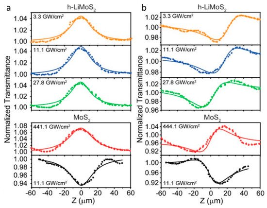
Figure 11. Open (a) and closed (b) aperture Z-scan measurements of h-LiMoS2 and MoS2 at different input laser power, indicated at the top left of each curve, showing saturable absorption and self-focusing behavior of h-LiMoS2 at a lower pumping power. Reprinted with permission from [112][31]. Copyright 2017 American Chemical Society.
6. Halide Perovskites
Halide perovskites, with the general crystal structure formula of ABX3 (A = organic ammonium cation, Cs+; B = Pb2+, Sn2+; X = Cl, Br, I), present some excellent optical and electrical properties such as low-temperature solution processability, long photocarrier lifetime, high fluorescence yield, wavelength tenability, and nonlinear response [113,114,115,116][32][33][34][35]. These unique and exciting properties make perovskites promising for application in optoelectronic devices, especially in photovoltaic operation and laser protection [117,118,119,120,121,122,123][36][37][38][39][40][41][42]. Figure 12a depicts the key structural factors of halide perovskites, these factors can form different properties of halide perovskites, such as absorption properties, the emission wavelength and charge carrier lifetimes, etc. Similar to TMDs, halide perovskites also have three different crystal structures of 100, 110, and 111 (Figure 12b), which can be used to construct different formations for its potentially diverse varieties of practical applications.
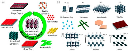
Figure 12. (a) The key structural factors that influence the properties of halide perovskites; Reprinted with permission from [113][32]. Copyright 2017 American Chemical Society. (b) (I) Representative crystal structures of halide perovskites in different dimensions; (II) nanoscale morphologies of halide perovskites; (III) schematic representation of the 2D organic–inorganic perovskites from different cuts of the 3D halide perovskite structure. L is a large organic cation, A is a regular cation such as Cs+ or MA+, B is a divalent metal cation such as Pb2+ or Sn2+, and X is a halide. Reprinted with permission from [114][33]. Copyright 2017 American Chemical Society.
The NLO response of organic−inorganic perovskites absorbers CH3NH3PbI3 was investigated by Snaith et al. and the typical SA was observed under the excitation of both 532 and 1064 nm [124][43]. The achieved nonlinear absorption coefficient and saturable intensity were −2.25 cm/MW, 12.71 GW/cm2 for CH3NH3PbI3 and −2.03 cm/MW, 12.61 GW/cm2 for CH3NH3PbI3−xClx, respectively (Figure 13a,b). The same OL response was also observed in the CH3NH3PbI3 perovskite nanosheets, in which the thickness was about 105 nm [123][42]. The achieved highest normalized transmittance value was 22.2% and the lowest saturable intensity was about 1.8 × 10³ GW/cm, which is much larger than the bulk perovskite sheets. By embedding the CH3NH3PbI3 film into the ring fiber laser, the organic–inorganic halide perovskites hybrid was prepared and showed the saturable absorption coefficients of the normalized transmittance value and saturable intensity were 13.58% and 6.4 MW/cm2, respectively [126][44]. All of these results suggest that the perovskites could find important applications in ultrafast photonics as a new type of NLO material.
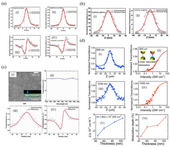
Figure 13. (a) Nonlinear absorption of CH3NH3PbI3 and CH3NH3PbI3−xClx samples under irradiation of a 1064 nm pulsed laser. (I) Experimental results and theoretical fitting for the nonlinear absorption of CH3NH3PbI3. (II) Experimental results and theoretical fitting for the nonlinear absorption of CH3NH3PbI3−xClx. (III) Experimental results and theoretical fitting for the nonlinear refractive index of CH3NH3PbI3. (IV) Experimental results and theoretical fitting for the nonlinear refractive index of CH3NH3PbI3−xClx; (b) Nonlinear absorption of CH3NH3PbI3 and CH3NH3PbI3−xClx samples in open aperture condition under irradiation of a 532 nm pulsed laser. (I) Experimental results and theoretical fitting for the nonlinear absorption of CH3NH3PbI3. (II) Experimental results and theoretical fitting for the nonlinear absorption of CH3NH3PbI3−xClx; Reprinted with permission from [124][43]. Copyright 2016 American Chemical Society. (c) (I) SEM image of the perovskite, and the inset shows the cross-sectional SEM image. (II) The linear transmittance spectrum of the perovskite. (III) The nonlinear open aperture and (IV) closed aperture/open aperture Z-scan measurement of the perovskite at 1562 nm, respectively; Reprinted with permission from [125][45]. Copyright 2017 American Chemical Society. (d) Nonlinear optical properties of CH3NH3PbI3 perovskite nanosheets. Z-scan profiles measured at (I) 800 and (III) 1030 nm. The normalized transmittance versus input peak intensity at (II) 800 and (IV) 1030 nm. The insets in panel b show the energy diagrams of the linear absorption and saturable absorption. (V) Nonlinear absorption coefficient β as a function of nanosheet thickness. (VI) Modulation depths of perovskite nanosheets with different thicknesses. Reprinted with permission from [126][44]. Copyright 2017 AIP Publishing.
References
- Chen, Y.; Bai, T.; Dong, N.; Fan, F.; Zhang, S.; Zhuang, X.; Sun, J.; Zhang, B.; Zhang, X.; Wang, J.; et al. Graphene and its derivatives for laser protection. Prog. Mater. Sci. 2016, 84, 118–157.
- Liu, Z.; Dong, N.; Jiang, P.; Wang, K.; Wang, J.; Chen, Y. Reduced Graphene Oxide Chemically Modified with Aggregation-Induced Emission Polymer for Solid-State Optical Limiter. Chem. Eur. J. 2018, 24, 19317–19322.
- Lei, W.; Liu, G.; Zhang, J.; Liu, M. Black phosphorus nanostructures: Recent advances in hybridization, doping and functionalization. Chem. Soc. Rev. 2017, 46, 3492–3509.
- Abate, Y.; Akinwande, D.; Gamage, S.; Wang, H.; Snure, M.; Poudel, N.; Cronin, S.B. Recent Progress on Stability and Passivation of Black Phosphorus. Adv. Mater. 2018, 30, 1704749.
- Castellanos-Gomez, A.; Vicarelli, L.; Prada, E.; Island, J.O.; Narasimha-Acharya, K.L.; Blanter, S.I.; Groenendijk, D.J.; Buscema, M.; Steele, G.A.; Alvarez, J.V.; et al. Isolation and characterization of few-layer black phosphorus. 2D Mater. 2014, 1, 025001.
- Hirsch, A.; Hauke, F. Post-Graphene 2D Chemistry: The Emerging Field of Molybdenum Disulfide and Black Phosphorus Functionalization. Angew. Chem. Int. Ed. 2018, 57, 4338–4354.
- Lu, S.B.; Miao, L.L.; Guo, Z.N.; Qi, X.; Zhao, C.J.; Zhang, H.; Wen, S.C.; Tang, D.Y.; Fan, D.Y. Broadband nonlinear optical response in multi-layer black phosphorus: An emerging infrared and mid-infrared optical material. Opt. Express. 2015, 23, 11183–11194.
- Guo, Z.; Zhang, H.; Lu, S.; Wang, Z.; Tang, S.; Shao, J.; Sun, Z.; Xie, H.; Wang, H.; Yu, X.-F.; et al. From Black Phosphorus to Phosphorene: Basic Solvent Exfoliation, Evolution of Raman Scattering, and Applications to Ultrafast Photonics. Adv. Funct. Mater. 2015, 25, 6996–7002.
- Shi, M.; Huang, S.; Dong, N.; Liu, Z.; Gan, F.; Wang, J.; Chen, Y. Donor-acceptor type blends composed of black phosphorus and C60 for solid-state optical limiters. Chem. Commun. 2018, 54, 366–369.
- Xu, Y.; Wang, Z.; Guo, Z.; Huang, H.; Xiao, Q.; Zhang, H.; Yu, X.-F. Solvothermal Synthesis and Ultrafast Photonics of Black Phosphorus Quantum Dots. Adv. Opt. Mater. 2016, 4, 1223–1229.
- Ji, J.; Song, X.; Liu, J.; Yan, Z.; Huo, C.; Zhang, S.; Su, M.; Liao, L.; Wang, W.; Ni, Z.; et al. Two-dimensional antimonene single crystals grown by van der Waals epitaxy. Nat. Commun. 2016, 7, 13352.
- Zhang, S.; Yan, Z.; Li, Y.; Chen, Z.; Zeng, H. Atomically thin arsenene and antimonene: Semimetal-semiconductor and indirect-direct band-gap transitions. Angew. Chem. Int. Ed. 2015, 54, 3112–3115.
- Zhang, S.L.; Xie, M.Q.; Li, F.Y.; Yan, Z.; Li, Y.F.; Kan, E.; Liu, W.; Chen, Z.F.; Zeng, H.B. Semiconducting Group 15 Monolayers: A Broad Range of Band Gaps and High Carrier Mobilities. Angew. Chem. Int. Ed. 2016, 128, 1698–1701.
- Wang, G.; Pandey, R.; Karna, S.P. Atomically thin group v elemental films: Theoretical investigations of antimonene allotropes. ACS Appl. Mater. Interfaces 2015, 7, 11490–11496.
- Zhao, M.; Zhang, X.; Li, L. Strain-driven band inversion and topological aspects in Antimonene. Sci. Rep. 2015, 5, 16108.
- Lee, J.; Tian, W.C.; Wang, W.L.; Yao, D.X. Two-Dimensional Pnictogen Honeycomb Lattice: Structure, On-Site Spin-Orbit Coupling and Spin Polarization. Sci. Rep. 2015, 5, 11512.
- Song, Y.; Liang, Z.; Jiang, X.; Chen, Y.; Li, Z.; Lu, L.; Ge, Y.; Wang, K.; Zheng, J.; Lu, S.; et al. Few-layer antimonene decorated microfiber: Ultra-short pulse generation and all-optical thresholding with enhanced long term stability. 2D Mater. 2017, 4, 045010.
- Zhang, F.; Wang, M.; Wang, Z.; Han, K.; Liu, X.; Xu, X. Excellent nonlinear absorption properties of β-antimonene nanosheets. J. Mater. Chem. C 2018, 6, 2848–2853.
- Zhao, G.; Zhang, F.; Wu, Y.; Hao, X.; Wang, Z.; Xu, X. One-Step Exfoliation and Hydroxylation of Boron Nitride Nanosheets with Enhanced Optical Limiting Performance. Adv. Opt. Mater. 2016, 4, 141–146.
- Chang, C.W.; Okawa, D.; Majumdar, A.; Zettl, A. Solid-State Thermal Rectifier. Science 2006, 314, 1121–1124.
- Golberg, D.; Costa, P.M.F.J.; Lourie, O.; Mitome, M.; Bai, X.D.; Kurashima, K.; Zhi, C.Y.; Tang, C.C.; Bando, Y. Direct Force Measurements and Kinking under Elastic Deformation of Individual Multiwalled Boron Nitride Nanotubes. Nano Lett. 2007, 7, 2146–2151.
- Chen, Y.; Zou, J.; Campbell, S.J.; Le Caer, G. Boron nitride nanotubes: Pronounced resistance to oxidation. Appl. Phys. Lett. 2004, 84, 2430–2432.
- Kumbhakar, P.; Kole, A.K.; Tiwary, C.S.; Biswas, S.; Vinod, S.; Taha-Tijerina, J.; Chatterjee, U.; Ajayan, P.M. Nonlinear Optical Properties and Temperature-Dependent UV-Vis Absorption and Photoluminescence Emission in 2D Hexagonal Boron Nitride Nanosheets. Adv. Opt. Mater. 2015, 3, 828–835.
- Xie, Z.; Wu, Y.; Sun, X.; Liu, S.; Ma, F.; Zhao, G.; Hao, X.; Zhou, S. Ultra-broadband nonlinear optical response of two-dimensional h-BN nanosheets and their hybrid gel glasses. Nanoscale 2018, 10, 4276–4283.
- Tan, C.; Cao, X.; Wu, X.J.; He, Q.; Yang, J.; Zhang, X.; Chen, J.; Zhao, W.; Han, S.; Nam, G.H.; et al. Recent Advances in Ultrathin Two-Dimensional Nanomaterials. Chem. Rev. 2017, 117, 6225–6331.
- Dong, N.; Li, Y.; Feng, Y.; Zhang, S.; Zhang, X.; Chang, C.; Fan, J.; Zhang, L.; Wang, J. Optical Limiting and Theoretical Modelling of Layered Transition Metal Dichalcogenide Nanosheets. Sci. Rep. 2015, 5, 14646.
- Qian, X.F.; Liu, J.W.; Fu, L.; Li, J. Quantum spin Hall effect in two-dimensional transition metal dichalcogenides. Science 2014, 346, 1344–1347.
- Sun, Y.; Wu, S.-C.; Ali, M.N.; Felser, C.; Yan, B. Prediction of Weyl semimetal in orthorhombic MoTe2. Phys. Rev. B 2015, 92, 161107.
- Qi, Y.; Naumov, P.G.; Ali, M.N.; Rajamathi, C.R.; Schnelle, W.; Barkalov, O.; Hanfland, M.; Wu, S.C.; Shekhar, C.; Sun, Y.; et al. Superconductivity in Weyl semimetal candidate MoTe2. Nat. Commun. 2016, 7, 11038.
- Shirodkar, S.N.; Waghmare, U.V. Emergence of ferroelectricity at a metal-semiconductor transition in a 1T monolayer of MoS2. Phys. Rev. Lett. 2014, 112, 157601.
- Tan, S.J.; Abdelwahab, I.; Ding, Z.; Zhao, X.; Yang, T.; Loke, G.Z.; Lin, H.; Verzhbitskiy, I.; Poh, S.M.; Xu, H.; et al. Chemical Stabilization of 1T’ Phase Transition Metal Dichalcogenides with Giant Optical Kerr Nonlinearity. J. Am. Chem. Soc. 2017, 139, 2504–2511.
- Chen, K.; Schunemann, S.; Song, S.; Tuysuz, H. Structural effects on optoelectronic properties of halide perovskites. Chem. Soc. Rev. 2018, 47, 7045–7077.
- Shi, E.; Gao, Y.; Finkenauer, B.P.; Akriti; Coffey, A.H.; Dou, L. Two-dimensional halide perovskite nanomaterials and heterostructures. Chem. Soc. Rev. 2018, 47, 6046–6072.
- Manser, J.S.; Christians, J.A.; Kamat, P.V. Intriguing Optoelectronic Properties of Metal Halide Perovskites. Chem. Rev. 2016, 116, 12956–13008.
- Cheng, P.; Zhan, X. Stability of organic solar cells: Challenges and strategies. Chem. Soc. Rev. 2016, 45, 2544–2582.
- Ju, M.G.; Dai, J.; Ma, L.; Zeng, X.C. Lead-Free Mixed Tin and Germanium Perovskites for Photovoltaic Application. J. Am. Chem. Soc. 2017, 139, 8038–8043.
- Kojima, A.; Teshima, K.; Shirai, Y.; Miyasaka, T. Organometal Halide Perovskites as Visible-Light Sensitizers for Photovoltaic Cells. J. Am. Chem. Soc. 2009, 131, 6050–6051.
- Gao, P.; Grätzel, M.; Nazeeruddin, M.K. Organohalide lead perovskites for photovoltaic applications. Energy Environ. Sci. 2014, 7, 2448–2463.
- Seo, J.; Noh, J.H.; Seok, S.I. Rational Strategies for Efficient Perovskite Solar Cells. Acc. Chem. Res. 2016, 49, 562–572.
- Yang, W.S.; Park, B.W.; Jung, E.H.; Jeon, N.J.; Kim, Y.C.; Lee, D.U.; Shin, S.S.; Seo, J.; Kim, E.K.; Noh, J.H.; et al. Iodide management in formamidinium-lead-halide–based perovskite layers for efficient solar cells. Science 2017, 356, 1376–1379.
- Sha, W.E.I.; Ren, X.; Chen, L.; Choy, W.C.H. The efficiency limit of CH3NH3PbI3 perovskite solar cells. Appl. Phys. Lett. 2015, 106, 221104.
- Sutherland, B.R.; Sargent, E.H. Perovskite photonic sources. Nat. Photon. 2016, 10, 295–302.
- Zhang, R.; Fan, J.; Zhang, X.; Yu, H.; Zhang, H.; Mai, Y.; Xu, T.; Wang, J.; Snaith, H.J. Nonlinear Optical Response of Organic–Inorganic Halide Perovskites. ACS Photon. 2016, 3, 371–377.
- Li, P.; Chen, Y.; Yang, T.; Wang, Z.; Lin, H.; Xu, Y.; Li, L.; Mu, H.; Shivananju, B.N.; Zhang, Y.; et al. Two-Dimensional CH3NH3PbI3 Perovskite Nanosheets for Ultrafast Pulsed Fiber Lasers. ACS Appl. Mater. Interfaces 2017, 9, 12759–12765.
- Jiang, G.; Miao, L.; Yi, J.; Huang, B.; Peng, W.; Zou, Y.; Huang, H.; Hu, W.; Zhao, C.; Wen, S. Ultrafast pulse generation from erbium-doped fiber laser modulated by hybrid organic–inorganic halide perovskites. Appl. Phys. Lett. 2017, 110, 161111.
More