Your browser does not fully support modern features. Please upgrade for a smoother experience.
Please note this is a comparison between Version 1 by Jiangang Liu and Version 2 by Beatrix Zheng.
Solution–processed organic solar cells (OSC) have been explored widely due to their low cost and convenience, and impressive power conversion efficiencies (PCEs) which have surpassed 18%. In particular, the optimization of film morphology, including the phase separation structure and crystallinity degree of donor and acceptor domains, is crucially important to the improvement in PCE. Considering that the film morphology optimization of many blends can be achieved by regulating the film–forming process, it is necessary to take note of the employment of solvents and additives used during film processing, as well as the film–forming conditions.
- organic solar cells
- solution process
- morphology
- film–forming kinetics
1. Introduction
Organic solar cells (OSCs) have been recognized as one of the most promising green devices to convert solar energy to electricity, which possesses the advantages of light weight, flexibility, processable printing and large–area production [1][2][3][4][1,2,3,4]. OSCs consist of an anode, cathode and active layer. By 2021, thanks to the favorable development of donor and acceptor materials, optimization of active layer morphology and maturity of processing technology, the OSCs have realized outstanding power conversion efficiency (PCE), over 18% for binary devices [5][6][7][8][9][10][11][12][5,6,7,8,9,10,11,12]. These devices based on a ternary active layer can achieve the same or better performance [13][14][15][16][17][18][19][13,14,15,16,17,18,19].
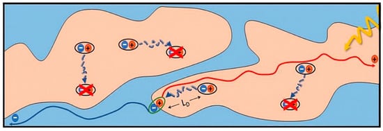
The performance of OSC devices is closely related to the morphology of the active layer, because it crucially affects the photophysical conversion process. The photophysical conversion process usually includes photon absorption (exciton generation), exciton diffusion, exciton separation, carrier transport and collection [20]. After the active layer absorbs a photon, the electron in the donor’s highest occupied molecular orbital (HOMO) is excited and jumps to the donor’s lowest unoccupied molecular orbital (LUMO) to form an electron–hole pair bounded by coulomb forces. Because of the strong binding energy (0.35~0.5 eV), the exciton cannot be separated through thermal vibration [21][22][21,22]. Therefore, the exciton separation can only rely on the electric field gravity provided by the built–in electric field at the donor/acceptor (D/A) interfaces. However, if the domain size is too large, some excitons cannot reach the D/A interfaces due to their short lifetime [23][24][23,24]. Only the excitons near the D/A interface (5~10 nm) can reach the interfaces and have the chance to dissociate into electrons and holes driven by the built–in electric field. Therefore, the suitable domain size is usually 10~20 nm in OSCs [25][26][25,26]. According to previous research, the molecular orientation of the donor and acceptor at the interface directly determines the driving forces of the built–in electric field [27]. When the orientation of the donor and acceptor is consistent, the coupling force between the donor and acceptor is large, leading to a strong built–in electric field, which is beneficial for exciton dissociation [28][29][30][28,29,30]. Furthermore, generated free electrons and holes need to transport to the corresponding anode and cathode through the pure acceptor and donor phases, respectively. Hence, the bi–continuous separated donor and acceptor phases, i.e., an interpenetrating network structure (Figure 1), is highly desirable for carrier transmission [31][32][33][34][35][31,32,33,34,35]. In addition, high carrier mobility ensures the efficiency of charge collection, hence a high crystallinity degree of the donor and acceptor is required because it reduces the energy barrier of charge transport and helps to obtain high carrier mobility [36][37][38][39][40][41][36,37,38,39,40,41]. Additionally, the donor and acceptor should be enriched at the anode and cathode, respectively, which can effectively reduce the bimolecular recombination, thereby improving the charge collection [42]. According to the relationship between the morphology of the active layer and the photoelectric process of devices, it is obvious that the active layer should possess a highly crystalline interpenetrating network with a proper domain size and face–on molecular orientation.
Therefore, on the basis of molecular tailoring [44][45][44,45], researchers have invented a variety of methods for optimizing the morphology of the active layer. One of most widely used effective methods is thermal annealing (TA), which can enhance the molecular stack and degree of crystallinity of the donor and acceptor [46][47][48][49][50][46,47,48,49,50]. For example, in P3HT:SF–HR–blend thin films, the diffraction intensity becomes much clearer, which means the degree of crystallinity of both the donor and acceptor increases dramatically after TA at 120 °C [51]. Similar to TA, solvent vapor annealing (SVA) is also an effective method to optimize the film morphology [52][53][54][55][56][52,53,54,55,56]. Hou et al. used a dichloromethane SVA–treated DRTB–T:IC–C6IDT–IC–based blend film for 60 s, and the ordered aggregation of donor and acceptor was promoted, which facilitated the formation of an interpenetrating network structure. This optimized phase separation structure is conducive to the exciton dissociation and carrier transport, boosting the PCE of the device from 5.03% to 9.08% [57]. However, it is a challenge to combine the two methods for practical large area manufacture, for TA is difficult to employ to treat flexible substrates of low glass transition temperature, and SVA is not compatible with the roll–to–roll process [58][59][58,59]. A number of research teams have recently made advances without using either method [60][61][62][63][60,61,62,63].
Furthermore, the morphology of the BHJ active layer closely depends on the film–forming process of solution processing [64][65][66][67][68][64,65,66,67,68]. During the evaporation of the solvent, the solution layer gradually evolves from the liquid state to solid state on the substrate, and the formed film is frozen in a thermodynamic metastable state. The film–forming process decides the film quenching depth of the frozen state. For example, through extending the film–forming time, the donor and acceptor molecules have sufficient time to diffuse and rearrange, leading to enhanced crystallinity of the film and increased domain sizes. If the donor and acceptor are precipitated simultaneously in a short time during the film–forming process, the degree of crystallinity of both the donor and acceptor is low due to the insufficient self–aggregating time. Therefore, controlling the kinetics of film–forming process can also regulate the morphology of the active layer.
This entry focuses on the influence of the film–forming kinetics process on the morphology of the active layer in OSCs, and the underlying mechanisms are revealed. Furthermore, methods used to regulate the film–forming kinetics process are summarized and representative examples are given and discussed to understand the key parameters of tuning the film–forming process. Finally, a future control and development of film–forming kinetics is briefly outlined, which may give some guidance to achieve a high PCE of OSCs. Here, we summarize in Table 1 the critical works on film–forming kinetics in OSCs, and the cartoon illustration is shown in Figure 2.
Figure 2. Cartoon illustration of film–forming dynamics.
Table 1. Summary of the performance of the OSC’s active layer previously reported (some full names corresponding to the abbreviations are listed below).
| Active Layer | Conditions | VOC [V] | JSC [mA cm−2] | FF [%] | PCEmax [%] | Ref. |
|---|---|---|---|---|---|---|
| P3HT:PCBM | Solvent CB | 0.64 | 1.63 | 52.3 | 0.58 | [69] |
| Additive ODT 0.5% | 0.55 | 8.23 | 68.8 | 3.13 | ||
| Additive CN 4% | 0.55 | 7.87 | 68.2 | 3.01 | ||
| PTzBI–Si:N2200 | Solvent CB | 0.87 | 4.58 | 51.14 | 2.04 | [70] |
| Solvent MTHF | 0.88 | 17.62 | 75.78 | 11.76 | ||
| PBDB–T:INPIC–4F | Cast under strong SV | 0.84 | 12.8 | 60.5 | 6.5 | [71] |
| Cast on 100 °C HS | 0.82 | 21.8 | 73.2 | 13.1 | ||
| PTB7–th:P(NDI2OD–T2) | Solvent CN | 0.79 | 1.24 | 55 | 0.6 | [72] |
| Solvent o–DCB | 0.77 | 6.82 | 51 | 2.86 | ||
| Solvent CB | 0.78 | 8.86 | 50 | 3.63 | ||
| Ph–DTDPo–OT:PBDB–T | Additive 1–CN 0.2% | 0.87 | 15.00 | 58.60 | 7.65 | [73] |
| Ph–DTDPo–OTE:PBDB–T | Additive 1–CN 0.5% | 0.88 | 18.28 | 68.57 | 10.98 | |
| Ph–DTDPo–TE:PBDB–T | Additive 1–CN 0.7% | 0.82 | 20.83 | 71.14 | 12.21 | |
| PDFQx3T:P(NDI2OD–T2) | Solvent CF | 0.80 | 10.58 | 60 | 5.11 | [74] |
| Solvent CB | 0.79 | 9.12 | 61 | 4.43 | ||
| Solvent DCB | 0.80 | 8.44 | 60 | 4.04 | ||
| Solvent XY | 0.79 | 7.91 | 61 | 3.83 | ||
| FTAZ:ITIC–Th | Solvent CF | 0.907 | 16.8 | 62.57 | 9.72 | [75] |
| Additive ODT:DIO 0.375%:0.125% | 0.922 | 17.78 | 66.64 | 11.15 | ||
| P3HT:O–IDTBR | Solvent CB | 0.77 | 8.81 | 64 | 4.45 | [42] |
| Additive TCB 2% | 0.76 | 13.49 | 70 | 7.18 | ||
| PCPDTBT/C71–PCBM | Solvent CB | 0.66 | 11.74 | 43 | 3.35 | [76] |
| Additive HS–C8H16–SH 2.5% | 0.64 | 14.48 | 49 | 4.50 | ||
| Additive Br–C8H16–Br 2.5% | 0.64 | 15.26 | 48 | 4.66 | ||
| Additive I–C8H16–I 2.5% | 0.61 | 15.73 | 53 | 5.12 | ||
| P3HT/PCBM | CB/tetralin 1:0.05 | – | 5.76 | 60 | 1.96 | [77] |
2. Summary and Perspectives
The photovoltaic performance of OSCs is closely related to the BHJ morphology of the active layer, because the crystallinity, molecular orientation, domain size and phase separation structure have a profound influence on the exciton dissociation, charge transport and collection. We know that the morphology of BHJ is a kinetically frozen structure. Hence, regulating the duration of the film–forming process, including solvent engineering and adjusting the substrate temperature, is an effective way to optimize the morphology of the active layer. The film–forming process contains solvent evaporation and solutes solidification, thus regulating the b.p. of solvents and spinning rate, and so is effective at optimizing the morphology. Specifically, prolonging the film–forming process could extend the duration of molecular diffusion, which is of benefit for the crystallization and phase separation; thus, high crystallinity and a large domain size with high phase purity were achieved. Moreover, the shortening of the film–forming process could promote the molecules to stay in a metastable state, in which the molecules tend to adopt face–on orientation. Furthermore, the selective solubility and high b.p. of the additive could also regulate the sequence of solidification between the donor and acceptor, promoting the formation of interpenetrating networks with optimized lateral phase separation. Overall, the examples demonstrated herein offer a rational guide to understanding the foundation of film–forming kinetics for optimizing the BHJ morphology of the active layer.
Presently, OSCs based on polymer/nonfullerene blends dominate the development of OSCs. The morphology optimization of the nonfullerene–based blend films empirically follows the various treatments originally developed in polymer/fullerene blends. Considering the different properties between nonfullerene and fullerene derivatives, such as solubility in solvent, miscibility between donor and acceptor and molecular diffusivity, morphology optimization should pay comprehensive attention to the molecular properties of the active layer, and rational morphology control treatments should be developed toward the combined goal of improved efficiency and increased stability. Additionally, solvent engineering is able to meet the requirements for the practical application of OSCs, such as the fabrication of large–area and flexible OSCs. Hence, thorough comprehension of film–forming kinetics in non–halogenated additives during large–area film–forming process should be taken into account to fabricate OSCs for their future application. The other important point is that existing research on film–forming kinetics does not elaborate on the relationship between kinetics and intermixed phases; although the study of intermixed phases is very complicated, kinetics may be used as a method to explore this field in the future.