Mechanical milling (MM) has attracted great attention as a powerful tool for the synthesis of a variety of sophisticated materials, including equilibrium, nonequilibrium (e.g., amorphous, quasicrystals, nanodiamonds, carbon nanotubes, nanocrystalline powders), and nanocomposite materials. The MM is a unique process in that it involves a solid-state interaction between the reactant materials’ fresh powder surfaces at room temperature. As a result, it has been used to fabricate alloys and compounds that are difficult or impossible to acquire using standard melting and casting processes.
- nanomaterials
- powder technology
- solid-state reaction
- nanocomposite materials
- hard nanomaterials
- gas-solid reaction
- reactive ball milling
1. Introduction
Despite the fact that conventional material categories (metals and metal alloys, ceramics, polymers, and composites) are incapable of meeting the demands of contemporary modern industries, a newcomer known as “advanced materials” has carved out a major niche in material functional classifications. Advanced materials, on the other hand, may be characterized by a number of techniques, depending on their properties and uses. They are materials that outperform conventional materials and are used to fabricate high-tech goods [1].
Nonetheless, while there are several fabrication techniques, which can be employed for producing conventional materials via hydrometallurgy, pyrometallurgy, and powder metallurgy approaches, none of these techniques is capable of readily preparing advanced materials. Over the past six decades, materials scientists have devised a number of synthesis processes and methods for the synthesizing of new material families, often referred to as advanced or “high-tech” materials, with distinguishing chemical, physical, and mechanical properties [2]. These novel techniques for processing and fabricating materials have enabled scientists to alter the subatomic structure of materials and tailor them to a desired and predetermined structure. To achieve high performance characterization, altering the structure of the materials (e.g., long- or short-range ordered) has an impact on the material’s overall properties. Additionally, modifying the morphological and microscopic characteristics of materials results in noticeable changes in their properties and behaviors [3,4][3][4]. It may be inferred that the way a material is prepared (material processing and fabrication) has an influence on its atomic arrangements and microscopic characteristics, which affects not only the product’s overall attributes, but also its performance and future uses [5].
Over the last few decades, materials scientists’ research has enabled us to produce a diverse spectrum of complex materials utilizing innovative preparation processes. The fabrication techniques for advanced materials can be broadly classified as follows: Mechanically aided approaches include the following: (1) mechanically driven solid-state reaction approaches; (2) thermally assisted approaches; (3) mechanically assisted approaches; (4) chemically assisted approaches; (5) lithographic approaches; (6) vapor deposition approaches; and (7) liquid-phase fabrication approaches [6]. Ball milling, rapid solidification, atomization, sputtering, chemical vapor deposition, electron beam physical vapor deposition, arc discharge, laser ablation, photolithography, nano-imprint lithography, sol-gel, atomic force microscope nanostencil, plasma enhanced chemical vapor deposition, plasma enhanced chemical vapor deposition, and atomic layer deposition are some examples of the preparation methods that are used to fabricate new materials [1].
2. Nanocrystalline and Nanopowders Prepared by Ball Milling Technique at KISR
2.1. Background
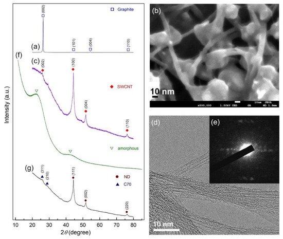
2.2. Nanodiamonds
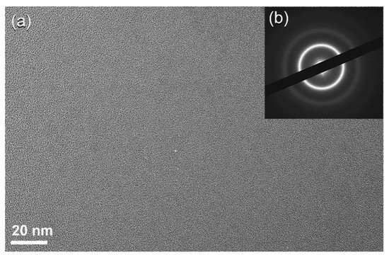
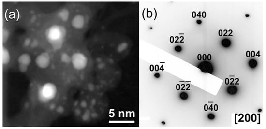
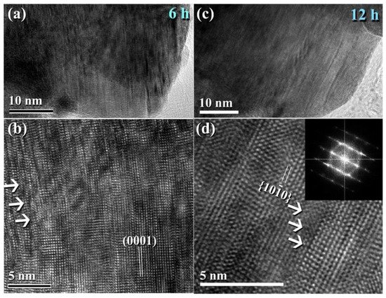
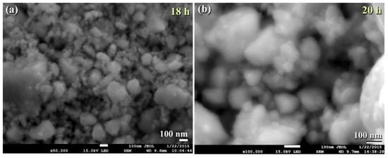
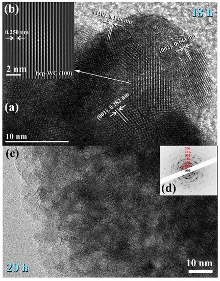
2.3. Tungsten Carbide
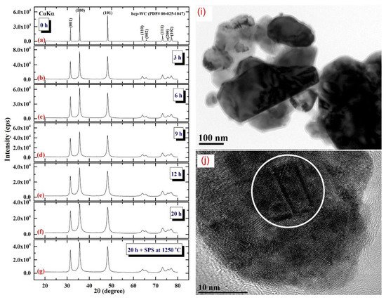
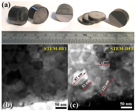
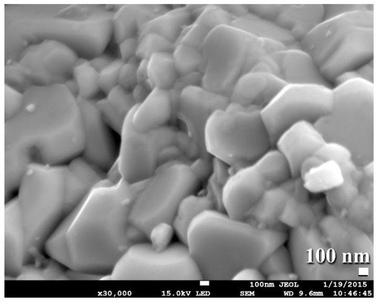
Consolidation of WC with Spark Plasma Sintering
References
- El-Eskandarany, M.S. Mechanical Alloying: Energy, Surface Protective Coating and Medical Applications, 3rd ed.; Elsevier: Oxford, UK, 2020.
- El-Eskandarany, M.S. Recent developments in the fabrication, characterization and implementation of MgH2-based solid-hydrogen materials in the Kuwait Institute for Scientific Research. RSC Adv. 2019, 9, 9907.
- Suryanarayana, C. Mechanical alloying: A novel technique to synthesize advanced materials. AAAS Res. 2019, 2019, 17.
- Polmear, I.; StJohn, D.; Nie, J.F.; Qian, M. Novel Materials and Processing Methods. Light Alloys, 5th ed.; Elsevier: Oxford, UK, 2017; pp. 461–514.
- El-Eskandarany, M.S.; Ali, N. Synthesizing of novel bulk (Zr67Cu33)100-xWx(x; 5–30 at%) glassy alloys by spark plasma sintering of mechanically alloyed powders. Molecules 2020, 25, 1906.
- El-Eskandarany, M.S.; Ali, N.; Saeed, M. Glass-forming ability and soft magnetic properties of (Co75Ti25)100-xFex(x; 0–20 at%) systems fabricated by SPS of mechanically alloyed nanopowders. Nanomaterials 2020, 10, 849.
- Gates, B.D.; Qiaobing, X.; Stewart, M.; Ryan, D.; Willson, C.G.; Whitesides, G.M. New approaches to nanofabrication: Molding, printing, and other techniques. Chem. Rev. 2005, 105, 1171–1196.
- Xiao, J.; Li, J.L.; Liu, P.; Yang, G.W. A new phase transformation path from nanodiamond to new-diamond via an intermediate carbon onion. Nanoscale 2014, 6, 15098–15106.
- Bovenkerk, H.; Bundy, F.; Hall, H.; Strong, H.M.; Wentorf, R.H. Preparation of diamond. Nature 1959, 184, 1094–1098.
- Danilenko, V.V. On the history of the discovery of nanodiamond synthesis. Phys. Solid State 2004, 46, 595–599.
- Yang, G.W.; Wang, J.B.; Liu, Q.X. Preparation of nano-crystalline diamonds using pulsed laser induced reactive quenching. J. Phys. Condens. Matter 1998, 10, 7923–7929.
- Frenklach, M.; Howard, W.; Huang, D.; Yuan, J.; Spear, K.E.; Koba, R. High-pressure synthesis of superhard and ultrahard materials. Appl. Phys. Lett. 1991, 59, 546–548.
- Mochalin, V.N.; Shenderova, O.; Ho, D.; Gogotsi, Y. The properties and applications of nanodiamonds. Nat. Nanotechnol. 2012, 7, 11–23.
- Welz, S.; Gogotsi, Y.; McNallan, M.J. Nucleation, growth, and graphitization of diamond nanocrystals during chlorination of carbides. Appl. Phys. 2003, 93, 4207–4209.
- Daulton, T.L.; Kirk, M.A.; Lewis, R.S.; Rehn, L.E. Production of nanodiamonds by high-energy ion irradiation of graphite at room temperature. Nucl. Instrum. Methods B 2001, 175, 12–20.
- Sun, L.T.; Gong, J.L.; Zhu, Z.Y.; Zhu, D.Z.; He, S.X.; Wang, Z.X.; Chen, Y.; Hu, G. Nanocrystalline diamond from carbon nanotubes. Appl. Phys. Lett. 2004, 84, 2901–2903.
- Caudillo, R.; Troiani, H.E.; Miki-Yoshida, M.; Marques, M.A.L.; Rubio, A.; Yacaman, M.J. A viable way to tailor carbon nanomaterials by irradiation-induced transformations. Radiat. Phys. Chem. 2005, 73, 334–339.
- Xiao, J.; Ouyang, G.; Liu, P.; Wang, C.X.; Yang, G.W. Reversible nanodiamond-carbon onion phase transformations. Nano Lett. 2014, 14, 3645–3652.
- Du, G.; Song, C.; Zhao, J.; Feng, S.; Zhu, Z. Solid-phase transformation of glass-like carbon nanoparticles into nanotubes and the related mechanism. Carbon 2008, 46, 92–98.
- Barnard, A.S.; Russo, S.P.; Snook, I.K. Coexistence of bucky diamond with nanodiamond and fullerene carbon phases. Phys. Rev. B 2003, 68, 073406.
- Tyler, T.; Zhirnov, V.V.; Kvit, A.V.; Kang, D.; Hren, J.J. Electron emission from diamond nanoparticles on metal tips. Appl. Phys. Lett. 2003, 82, 2904–2906.
- Frenklach, M.; Chang, R.P.H. Nucleation of diamond films on surfaces using carbon clusters. Appl. Phys. Lett. 1991, 59, 546–548.
- Vandenbulcke, L.; Gries, T.; Rouzaud, J.N. Nanodiamonds in dusty low pressure plasmas. Appl. Phys. Lett. 2009, 94.
- Zheng, J.; Lienhard, B.; Doerk, G.; Cotlet, M.; Bersin, E.; Kim, H.S.; Byun, Y.C.; Nam, C.Y.; Kim, J.; Black, C.T.; et al. Top-down fabrication of high-uniformity nanodiamonds by self-assembled block copolymer masks. Sci. Rep. 2019, 9, 6914.
- Greiner, N.R.; Phillips, D.S.; Johnson, J.D.; Volk, F. Diamonds in detonation soot. Nature 1988, 333, 440–442.
- Zhou, A.F.; Pacheco, E.; Zhou, B.; Feng, P.X. Size-Dependent Electrical Transport Properties in Conducting Diamond Nanostripes. Nanomaterials 2021, 11, 1765.
- El-Eskandarany, M.S. Method for Synthesizing Nanodiamonds. US Patent 9,540, 245B1, 10 January 2017.
- Yan, Z.X.; Cai, M.; Shen, P.K. Nanosized tungsten carbide synthesized by a novel route at low temperature for high performance electrocatalysis. Sci. Rep. 2013, 3, 1646.
- El-Eskandarany, M.S. Fabrication of nanocrystalline WC and nanocomposite refractory materials at room temperature. J. Alloy. Compd. 2000, 296, 175–182.
- El-Eskandarany, M.S.; El-Mahdy, A.A.; Ahmed, H.A.; Amer, A.A. Synthesis and characterizations of ball-milled nanocrystalline wc and nanocomposite WC-Co powders and subsequent consolidations. J. Alloy. Compd. 2000, 312, 315–325.
- Bicho, R.C.; Scott-Fordsm, J.J.; Mónica, J.B.A. Multigenerational Exposure to WCCo Nanomaterials—Epigenetics in the Soil Invertebrate Enchytraeus crypticus. Nanomaterials 2020, 10, 836.
- Li, W.; Yang, X.; Xiao, J.; Hou, Q. Effect of WC mass fraction on the microstructure and friction properties of WC/Ni60 laser cladding layer of brake discs. Ceram. Int. 2021, 47, 28754–28763.
- El-Eskandarany, M.S.; Al-Hazza, A.; Al-Hajji, A.A. HRTEM and nanoindentation studies of bulk WC nanocrystalline materials prepared by spark plasma sintering of ball-milled powders. J. Mater. Eng. Perform. 2017, 26, 124–133.
- Maier, K.; Klünsner, T.; Krobath, M.; Pichler, P.; Marsoner, S.; Echer, W.; Czettl, C.; Schäfer, J.; Ebner, R. Creep behavior of WC-12 wt% Co hardmetals with different WC grain sizes tested in uniaxial tensile and compression step-loading tests at 700 °C and 800 °C. Int. J. Refract. Met. Hard Mater. 2021, 100, 105633.
- El-Eskandarany, M.S.; Omori, M.; Ishikuro, M.; Konno, T.J.; Takada, K.; Sumiyama, K.; Hirai, T.; Suzuki, K. Synthesis of full-density nanocrystalline tungsten carbide by reduction of tungstic oxide at room temperature. Met. Trans. A 1996, 27, 4210–4213.
- Enneti, R.K. Synthesis of nanocrystalline tungsten and tungsten carbide powders in a single step via thermal plasma technique. Int. J. Refract. Met. Hard Mater. 2015, 53.
- Fang, Z.Z.; Wang, X.; Ryu, T.; Hwang, K.S.; Sohn, H.Y. Synthesis, sintering, and mechanical properties of nanocrystalline cemented tungsten carbide—A review. Int. J. Refract. Met. Hard Mater. 2009, 27, 288–299.
- Fecht, H.J. Nanostructure formation by mechanical attrition. Nanostructured Mater. 1995, 6, 33–42.
- Maizza, G.; Grasso, S.; Sakka, Y.; Noda, T.; Ohashi, O. Relation between microstructure, properties and spark plasma sintering (SPS) parameters of pure ultrafine WC powder. Sci. Technol. Adv. Mater. 2007, 8, 644–654.
