Highly sensitive and selective gas and volatile organic compound (VOC) sensor platforms with fast response and recovery kinetics are in high demand for environmental health monitoring, industry, and medical diagnostics. Among the various categories of gas sensors studied to date, field effect transistors (FETs) have proved to be an extremely efficient platform due to their miniaturized form factor, high sensitivity, and ultra-low power consumption. Despite the advent of various kinds of new materials, silicon (Si) still enjoys the advantages of excellent and reproducible electronic properties and compatibility with complementary metal–oxide–semiconductor (CMOS) technologies for integrated multiplexing and signal processing. This review gives an overview of the recent developments in Si FETs for gas and VOC sensing. We categorised the Si FETs into Si nanowire (NW) FETs; planar Si FETs, in which the Si channel is either a part of the silicon on insulator (SOI) or the bulk Si, as in conventional FETs; and electrostatically formed nanowire (EFN) FETs. The review begins with a brief introduction, followed by a description of the Si NW FET gas and VOC sensors. A brief description of the various fabrication strategies of Si NWs and the several functionalisation methods to improve the sensing performances of Si NWs are also provided. Although Si NW FETs have excellent sensing properties, they are far from practical realisation due to the extensive fabrication procedures involved, along with other issues that are critically assessed briefly. Then, we describe planar Si FET sensors, which are much closer to real-world implementation. Their simpler device architecture combined with excellent sensing properties enable them as an efficient platform for gas sensing. The third category, the EFN FET sensors, proved to be another potential platform for gas sensing due to their intriguing properties, which are elaborated in detail. Finally, the challenges and future opportunities for gas sensing are addressed.
- silicon FETs
- gas sensor
- VOC sensor
- silicon nanowire
1. Introduction
Application of gas and chemical sensors is ubiquitous in biomedical research, preventive healthcare, food safety, automotive and chemical industries, homeland security, environmental health and pollution monitoring [1][2][3][4][5][1,2,3,4,5]. Thus, there is always an urgent demand for the development of a chemical/gas sensor with a low detection limit (ideally trace-level molecule detection), high sensitivity, fast response and recovery times, minimum drift, large dynamic range and excellent selectivity to the target analyte under different ambients (dry/humid). In addition to this, with the recent boom of the Internet of Things (IoT), the need for reliable and miniaturized chip-scale gas sensors with ultra-low power consumption has become increasingly important [6][7][6,7]. Among the various categories of gas sensors (resistive, nanoelectromechanical systems, etc.) [6][8][9][10][6,8,9,10] that can meet chip-scale miniaturization and low-power operation without a compromise on the sensitivity or selectivity, sensors based on field effect transistors (FETs) [1] have shown significant promising potential. A FET is a three-terminal active device in which the conduction current in the semiconductor channel is modulated by a third terminal, called the gate electrode, apart from the usual source and drain electrodes. Signal amplification is achieved by induced electric fields due to the presence of chemical analytes, which allow signals from trace molecules to be detected. To date, different types of FET configurations have been developed to gain more control of the sensing performances [1][11][1,11]. A growing interest in FET technology has enabled various materials, such as organic semiconductors [12][13][14][12,13,14], inorganic semiconducting nanowires and thin films [15][16][17][18][15,16,17,18], carbon nanotubes [19], graphene [20] and transition metal dichalcogenides [21] to be integrated into this platform for sensing applications. Enhanced sensing performances in terms of sensitivity, response and recovery times have been achieved by such sensors due to the large surface-to-volume ratio of these materials, enabled by nanoscale dimensions coupled with the FET architecture. However, among these, monocrystalline Si and its derivatives still enjoy the advantages of having excellent and reproducible electronic properties and compatibility with complementary metal–oxide–semiconductor (CMOS) technologies for integrated multiplexing and signal processing [22]. Advanced growth, lithographic and nanofabrication techniques can produce nanostructured Si elements for improved performance in sensing devices. Further, surface modification or chemical functionalisation of these devices allow them to achieve a desired selectivity to a specific analyte.
This review article highlights the recent advances in the development of Si FET devices for sensing gas and VOC for various applications. The article is divided into several sections. In the next section, a wide description of Si NW-based FET sensors is presented and discussed. In the third section, sensors based on planar Si FETs fabricated out of SOI or bulk Si are reviewed; this approach overcomes some of the limitations observed with Si NW-based FETs. In the fourth section, EFN FET sensors are discussed. Recent works over the past decade are highlighted in each section. In some cases, wherever relevant, details about the device architecture, functionalisation and sensing principles are discussed for the benefit of readers. The final section provides a brief overview of the challenges and opportunities for research associated with this field, and some perspectives on future developments. Most of the studies related to Si sensors are limited to sensing and monitoring chemical and biological species in aqueous solutions using Si NW sensors. To the best of our knowledge, only two reviews on Si NWs for gas sensing have been published in the recent past [5,23], but other types of Si FET gas sensors have not been reviewed in a comprehensive manner until now. We believe that this article will give a broad outlook to readers on the recent technological advancements in Si FET-based sensors for gas and VOC sensing and pave the way for future developments of gas and VOC sensors.
2. Si NW FETs for Gas Sensing
Bare Si NWs have been used widely both in resistive and FET configurations for detection of various gases and vapours. However, to achieve selectivity, it is essential to modify the surfaces of these NWs through different approaches to create hybrid structures offering enhanced sensor performance metrics.
Haick’s group has worked extensively on Si NWs and their modification with various organic materials [24][25][26][27][26,38,39,40] in order to impart sensitivity to various VOCs, both polar and nonpolar. Paska et al. [24][28][26,41] utilised Si NWs to demonstrate selectivity towards nonpolar VOCs by modifying the Si NWs’ surface with a silane monolayer such as hydrophobic organic hexyltrichlorosilane (HTS), which otherwise has limited sensitivity towards the nonpolar VOCs. This limited sensitivity to the nonpolar VOCs can be attributed to weak adsorption of nonpolar VOCs in molecule-free sites and lack of suitable nonpolar organic functionalities, which facilitates more energy transfer from nonpolar gases (9.2 kJ/mol) compared to polar functional groups [29][42]. In addition, a high density of surface states at the SiO 2/Si interface interferes with the molecular gating, and the high density of trap states at the air/SiO 2 interface in the form of SiO − attracts water molecules and degrades the device performance [24][26]. The device was exposed to a number of polar (ethanol, butanol, and hexanol) and nonpolar molecules (hexane, octane, and decane), along with humidity. Figure 1 i shows the schematic of the Si NW FET device that was modified with the 0% cross-linked HTS monolayer. Figure 1 ii shows the conductivity change of the device for all the molecules tested. It can be seen that all polar VOCs exhibited a nonzero positive conductivity change at high negative voltages. In contrast, the water molecules showed a nonzero negative conductivity change at high negative voltages. The sensitivity of the HTS–Si NW FET sensor towards nonpolar VOCs exceeded the sensitivity towards polar molecules at approximately the same concentrations. This could be attributed to the formation of a dense HTS monolayer that successfully detected the nonpolar VOCs and prevented polar VOCs from reaching the Si NW surface. This can be explained in terms of an indirect sensor–VOC interaction, whereby the nonpolar VOC molecules induce conformational changes in the organic monolayer, affecting (i) the dielectric constant and/or effective dipole moment of the organic monolayer, and/or (ii) the density of charged surface states at the SiO 2/monolayer interface, which in turn modulate the conductivity of the Si NW. In comparison, a direct electrostatic interaction between the Si NW and polar VOCs possibly changes the Si NW charge carrier concentration [24][28][26,41].
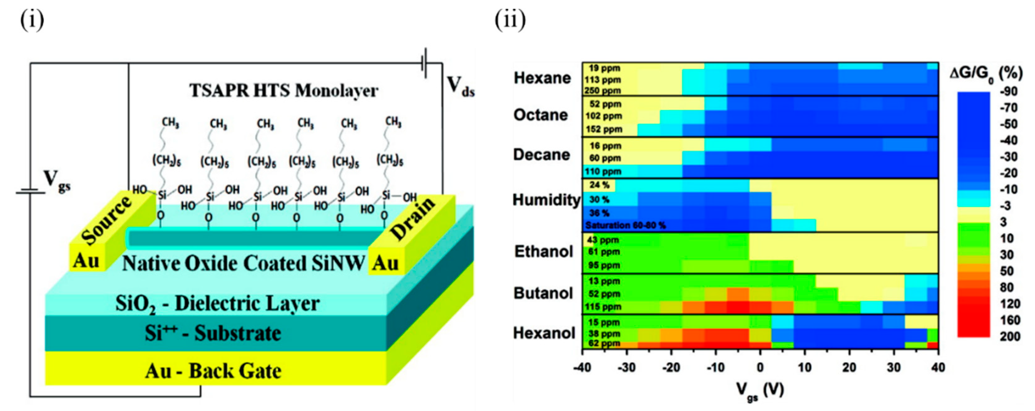 Figure 1. (i) Schematic of a back-gated Si NW FET configuration coated with a 0% cross-linked HTS monolayer. (ii) Counter map of the relative conductivity change of the device at various gate voltages for the polar and nonpolar VOCs at different concentrations. In the case of hexanol, the gate voltage shifted to a lower value, and the relative conductivity change became positive. Adapted and reprinted with permission from [24][26]. Copyright (2011) American Chemical Society.
Wang et al. of Haick’s group [27][40] further explored the effect of the end functional group of the molecular layer with the same backbone on the sensing properties of VOCs. Threshold voltage ( V th ) and hole mobility ( μ h ) served as the sensing parameters for various VOCs. Changes in V th (∆ V th ) and μ h (∆ μ h ) showed a dependence on the VOC concentration. However, the direction of the V th shift depended on the end group of the molecular layer. They developed a model based on dipole sensing to explain the sensing mechanism and classified the interaction between the molecular layers and VOCs into three different categories: (1) dipole−dipole interaction between the molecular layer and the polar VOCs; (2) induced dipole−dipole interaction between the molecular layers and the nonpolar VOCs; and (3) molecule tilt as a result of VOC diffusion between the chains of the molecular layer. VOC adsorption on molecular layers could occur in two ways: they could either be adsorbed on the surface of the molecule, and/or they could diffuse between the chains of the molecular layers. The dipole moment orientation of the adsorbed VOCs were determined by the electron-donating or -withdrawing nature of the end functional group, and this in turn determined the direction of the shift in V th . On the contrary, the type and density of the functional groups played a crucial role in determining the diffusion process of the VOCs between the chain of the molecular layers, and contributed mainly to ∆ μ h responses. This finding could be extremely useful in designing Si NW FET sensors with molecular layers to selectively detect nonpolar VOCs that otherwise do not participate in charge transfer with the molecular layers.
Wang et al. [26][39] further studied the effect of chain length in the organic monolayers on the sensing performance to both polar and nonpolar VOCs. To demonstrate this, they fabricated Si NW FETs functionalised with organic layers that had a similar end group (methyl) and amide bridge bond, but differed in the alkyl chain length. Changes in the threshold voltage (Δ V th ) and relative hole mobility (∆ μ h / μ h-a ) were observed to have a direct correlation with the exposed VOC concentration. ∆ μ h is the change in mean hole mobility due to VOC exposure, and μ h-a is the mean hole mobility in air before VOC exposure. Interestingly, when exposed to a specific VOC concentration, the response in Δ V th increased with the chain length of the organic molecule, whereas Δ μ h / μ h-a did not show any dependence on the same. An electrostatic model was developed to explain the results, which suggested that the sensor response in Δ V th was determined by the VOC concentration, VOC vapor pressure, VOC–molecular layer binding energy, and VOC adsorption-induced dipole moment changes of the molecular layer. In addition, a longer chain length of the molecular layer and relative low second-layer amide-reaction ratio enabled a large intermolecular space of the long-chain molecular layer that facilitated adsorption of more VOC molecules compared to short chain molecular layer, thus contributing to the increased Δ V th response to VOCs. The diffusion process of VOCs between the chain of molecular layers that contribute to μ h responses was not so dominantly affected by the alkyl chain length, thus explaining the absence of a systematic relationship between the Δ μ h / μ h-a and the chain length of the molecular layer.
3. Planar Si FETs for Gas Sensing
Although Si NW-based FETs have proved to be a promising platform for gas sensing, it is not feasible to implement them using large-scale conventional fabrication processes. Despite tremendous advances in the field of Si NWbased sensors, many challenges still inhibit a widespread technical and commercial use of these sensors, and limited them to academic research only. An alternative that is compatible with mass production is the use of the planar Si-based FETs fabricated out of SOI or bulk Si.
In 2017, Fahad et al. [6] fabricated chemically sensitive FETs (CS-FETs) (using a top-down, CMOS-compatible fabrication process) based on a 3.5 nm thin Si channel on an insulator ( Figure 2 i). These ultrathin Si channels functioned as fully depleted transistors and formed the driving force of low-power digital electronics. Instead of an electrically active gate layer, these FETs had an electrically nonconductive, chemically sensitive layer that on interaction with the target analyte, caused a chemical gating effect and modulated the conduction current in the Si channel, and shifted the channel threshold voltage. This CSFET could act as a generic sensing platform, and by appropriate choice of chemically sensitive layers (deposited through multiple processing steps) could detect a wide range of gases. In their work, they demonstrated sensing of H 2S, H 2 and NO 2 using Pd 0.3nm Au 1nm , Ni 0.3nm Pd 1nm , and Ni 1nm , respectively. Figure 2 ii shows the cross sectional transmission electron microscopy (TEM) image of the Pd–Au CSFET. These CS-FETs operated as junction-less n-channel transistors in which the channel doping (degenerate doping) level was identical to the source and the drain. The charge carriers in the 3.5 nm Si channel could be fully depleted on gas exposure, thus modulating the output current by orders of magnitude. The sensing principle was based on the work function modulation of the chemically sensitive layer, causing a band realignment that shifted the threshold voltage ( Figure 2 iii). The interaction of the gas analyte determined the nature of the sensing response. For example, reducing gases (like H 2S) (as depicted in Figure 2 iv) caused a negative threshold voltage shift and current increase in n-channel devices, while a current decrease and positive threshold voltage shift took place following exposure to oxidizing gases (e.g., NO 2).
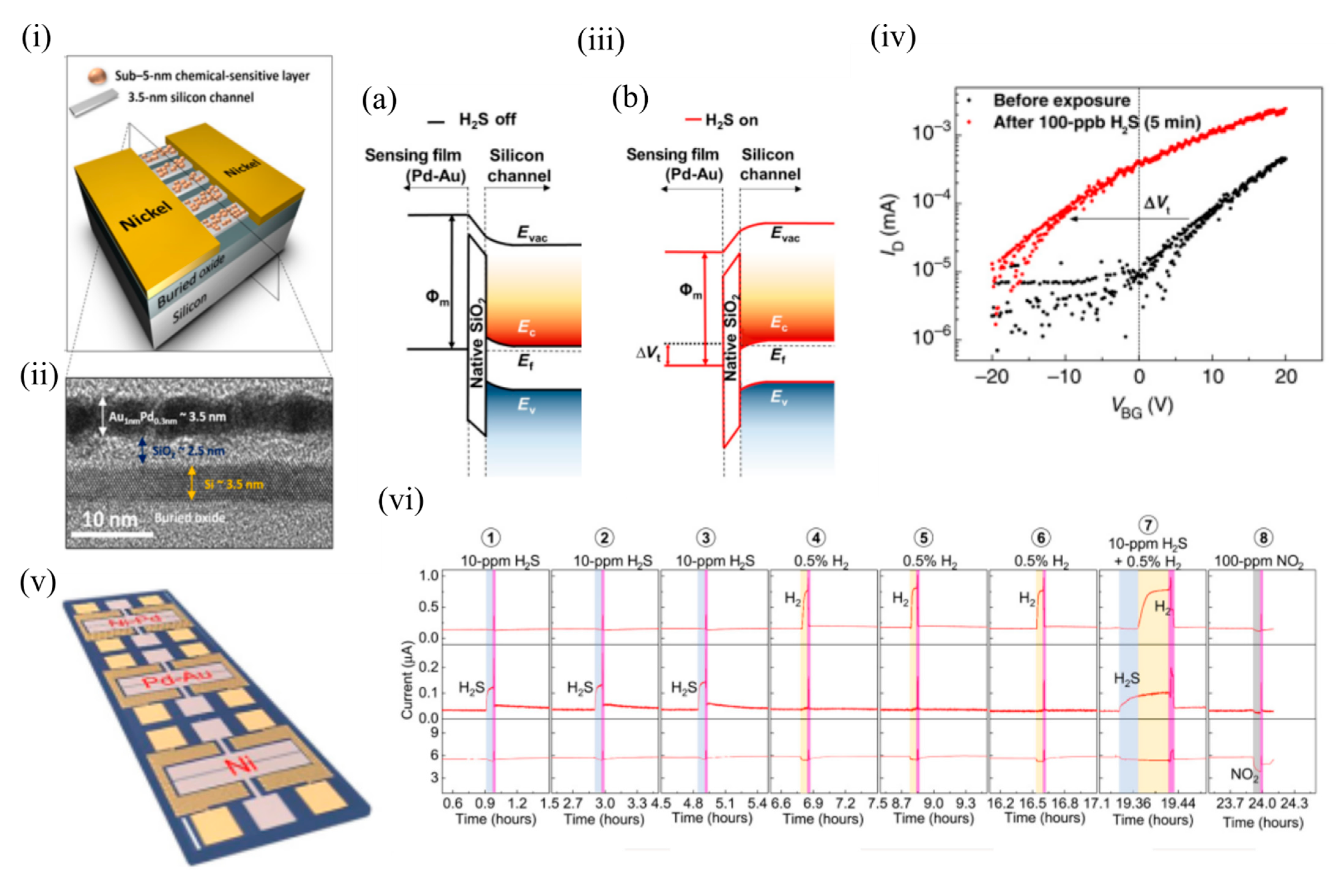 Figure 2. The CS-FET gas sensor. (i) Schematic illustration of a single CS-FET device decorated with NPs. (ii) Cross-sectional TEM image taken across the ultrathin silicon channel as shown in (i). (iii) Schematic illustration of the band edge alignment across the Pd–Au sensing layer and ultrathin Si channel in a H2S-sensitive CS-FET (a) before H2S exposure and (b) after 100 ppb of H2S exposure. Evac, vacuum energy level; Ec, bottom of the Si conduction band energy level; Ev, top of the silicon valence band energy level; Ef, silicon Fermi-level energy. (iv) FET transfer characteristics (ID-VBG) of a H2S-sensitive CS-FET demonstrating Vt shift due to 100-ppb H2S (in air) exposure (VDS = 10 mV). (v) Optical microscopy image of a single CS-FET array chip. Scale bar = 200 μm. (vi) Real-time multiplexed sensing data for different gases (VDS = 25 mV; VBG = 0 V; relative humidity, ~40%; T ≈ 25 °C). Adapted and reprinted from [6] under the Creative Commons Attribution-NonCommercial license.
It is a challenge to detect accurate concentrations of gas in ambient with dynamically changing relative humidity and temperature, and these are the major limiting factors for air-quality monitoring and medical diagnosis. Most of the active sensing materials are responsive to slight environmental changes, which consequently change the sensor signal and make it difficult to determine the actual gas concentration in real conditions. Thus, it is of utmost importance to design gas sensors that are selective to a desired analyte for a wide range of temperatures and humidity. Various computational methods (involving signal processing utilising advanced machine-learning techniques) and experimental techniques have been found to circumvent this problem, but most of them focused on either sensor response to gas at different RH conditions or response to various humidity levels, and did not consider them as a coupled problem. The conventional metal–oxide sensors operate at a high temperature > 200 °C through use of integrated heaters that also help in removal of water molecules, but suffer from high power consumption. The CS-FETs developed by Javey’s group [30][48] made an attempt to overcome this problem through the use of integrated localon-chip microheaters around the sensors ( Figure 3 i(a,b)) and operate them at a slightly higher temperature than room temperature. In order to prove selectivity against humidity, they considered platinum NPs on trichloro (1H, 1H, 2H, 2H-perfluorooctyl) silane (FOTS) as the active sensing material for the detection of H 2 gas. Figure 3 i(c) depicts a top-view TEM image of Pt/FOTS on SiO 2 grids. Previous studies confirmed the strong interaction between Pt and H 2 gas, and increased sensor performance metrics with FOTS underneath Pt. Detection of low concentration (in ppm levels) was demonstrated, but was highly sensitive to RH change, thus making it a suitable candidate for testing this technique. Capillary condensation was expected to occur between the NPs ( Figure 3 i(d)), and the approximate RH level that marked the onset of this phenomenon was calculated to be 59%. They observed that with increasing microheater power (which had a linear relation with temperature), the sensor response to RH change from 50 to 90% decreased exponentially ( Figure 3 ii). A negligible sensor response of 11.6% was observed at a power of 372 mW corresponding to a chip temperature of 37 ± 3 °C. This was because with an increase of surface temperature, the evaporation rate of any condensed water increases; consequently the probability of water molecules adhering to the sensing material also decreases with increasing chip temperature, according to Le Chatelier’s principle [31][49]. A relatively low chip temperature (<100 °C) was sufficient enough to eliminate humidity, as water molecules could be evaporated instead of being boiled off. In addition, the high surface-to-volume ratio of the NPs allowed a high evaporation rate, unlike thick films in MOS sensors and other FET-based gas sensors. The sensitivity to H 2 (250 ppm and 1000 ppm) hardly changed at RH levels of 50 and 90%, as depicted in Figure 3 iii. The CS-FET also exhibited good selectivity against other gases like methane, carbon dioxide, ammonia, nitrogen dioxide, and sulphur dioxide, except for hydrogen sulphide, which is known for its poisoning action on catalysts like Pt [32][33][34][50,51,52]. Apart from the use of the microheaters to eliminate the effect of humidity on the sensor response, they also helped to maintain constant sensitivity with changing ambient temperature, as depicted in Figure 3 iv,v. This further simplified the calibration process and promised low-concentration-level detection even at lower ambient temperatures for practical usage. In addition, with continuous microheater operation for 10 days at a chip temperature of 51 ± 6 °C, a negligible drift was observed, which ensured no material degradation of either the active material (Pt-FOTS) or the silane layer. The use of integrated microheaters to eliminate the response to humidity was further extended to CS-FETS with InOx thin film (~1.5 nm) as the electrically active gate material for NO 2 sensing. The group further intends to improve upon the heating power needed to reach the chip temperature levels in order to eliminate humidity levels by working on various aspects of the microheater material selection and design. Further systematic studies with a library of sensing materials are required to see their long-term sustainability to the emitted heat from the microheaters. Nonetheless, the study provided a platform to reduce the practical challenges associated with sensing in ambient conditions with different humidity and temperature levels.
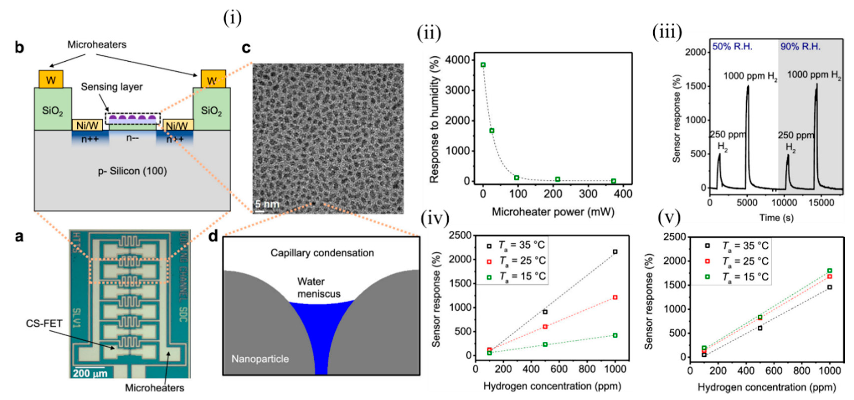 Figure 3. The CS-FET gas senor with integrated microheaters. (i) (a) Optical micrograph of the CS-FET chip with the microheaters, and (b) schematic of the cross section. (c) Top-down TEM image of Pt/FOTS on SiO2 grids. (d) Schematic of capillary condensation of water occurring in the cavity between decorated NPs. (ii) Sensor response of the CS-FET to a relative humidity change from 50 to 90% vs. microheater power. (iii) Sensor response to 250 and 1000 ppm of H2 at relative humidity levels (R.H.) of 50 and 90% with VD = 0.65 V, at a chip temperature of 64 ± 8 °C. (iv) Sensor response vs. H2 concentration in different ambient temperatures (Ta) at VD = 0.6 V with microheaters off, and (v) with microheaters on at 372 mW. Adapted and reprinted with permission from [30][48]. Copyright (2019) American Chemical Society.
Yuan et al. of the same group demonstrated multiplexed gas detection at room temperature associated with food spoilage through the use of an integrated CS-FET array [35][53]. NH 3 and H 2S acted as marker gases for spoilt high-protein foods like eggs, diary, and meat and hence served as indicators for freshness of these foods. Sensors should be able to detect these gases at very low concentrations (less than 100 ppb) to suggest the possible onset of spoilage at an early stage. In addition, humidity plays an important role in affecting food storage and spoilage, and hence should be simultaneously monitored along with NH 3 and H 2S. N-doped bulk CS-FETs were developed with electrically floating thin films of ruthenium (Ru), Ag, and SiOx to selectively detect NH 3, H 2S and humidity respectively, through a chemical gating effect. These materials were chosen for the following reasons: Ru is known to show catalytic effects towards NH 3 [35][36][37][53,54,55]; Ag is known to bind strongly to sulphur-containing compounds [38][56]; and the abundant oxygen vacancies formed due to rapid deposition of SiOx react strongly with humidity [39][57]. Figure 4 i depicts the device structure of such CS-FETs. For practical food-spoilage monitoring, egg and pork belly were chosen as representative samples. Prior to that, each sensor in the array was tested at various concentrations of NH 3, H 2S, and humidity to determine sensitivity and selectivity, as depicted in Figure 4 ii. The limit of detection achieved was 10 ppb for both gases, which was well below the desired limit, as stated previously. They attributed the origin of the sensor signal to work-function variation of the electrically floating gate materials. The sensitivity obtained with NH 3 and H 2S FETs was superior to recently published results. The authors also checked for stability, hysteresis and long-term performance of these sensors. All the sensors exhibited good stability both at low and high concentrations, with slight drift in the baseline signal between cycles. Low hysteresis was also observed, and sensor performance was also retained after a month. The inorganic sensing layers allowed more robustness and retention of sensor performances beyond a long period of time. The multi-CS-FET array was also tested for selectivity towards other interfering common air pollutant gases such as CO, SO 2, HCHO and NO 2, and the sensors exhibited negligible responses to these gases, thus proving its strong potential application in food spoilage and waste monitoring. The CSFET array was then integrated with a custom printed circuit board and circuitry to perform controlled measurements of food spoilage. With suitable choice of functional materials, the platform can further serve as a portable system to detect various gaseous markers of lung or gastrointestinal diseases at ppb levels present in exhaled breath, or to monitor toxic gas leaks in industrial plants.
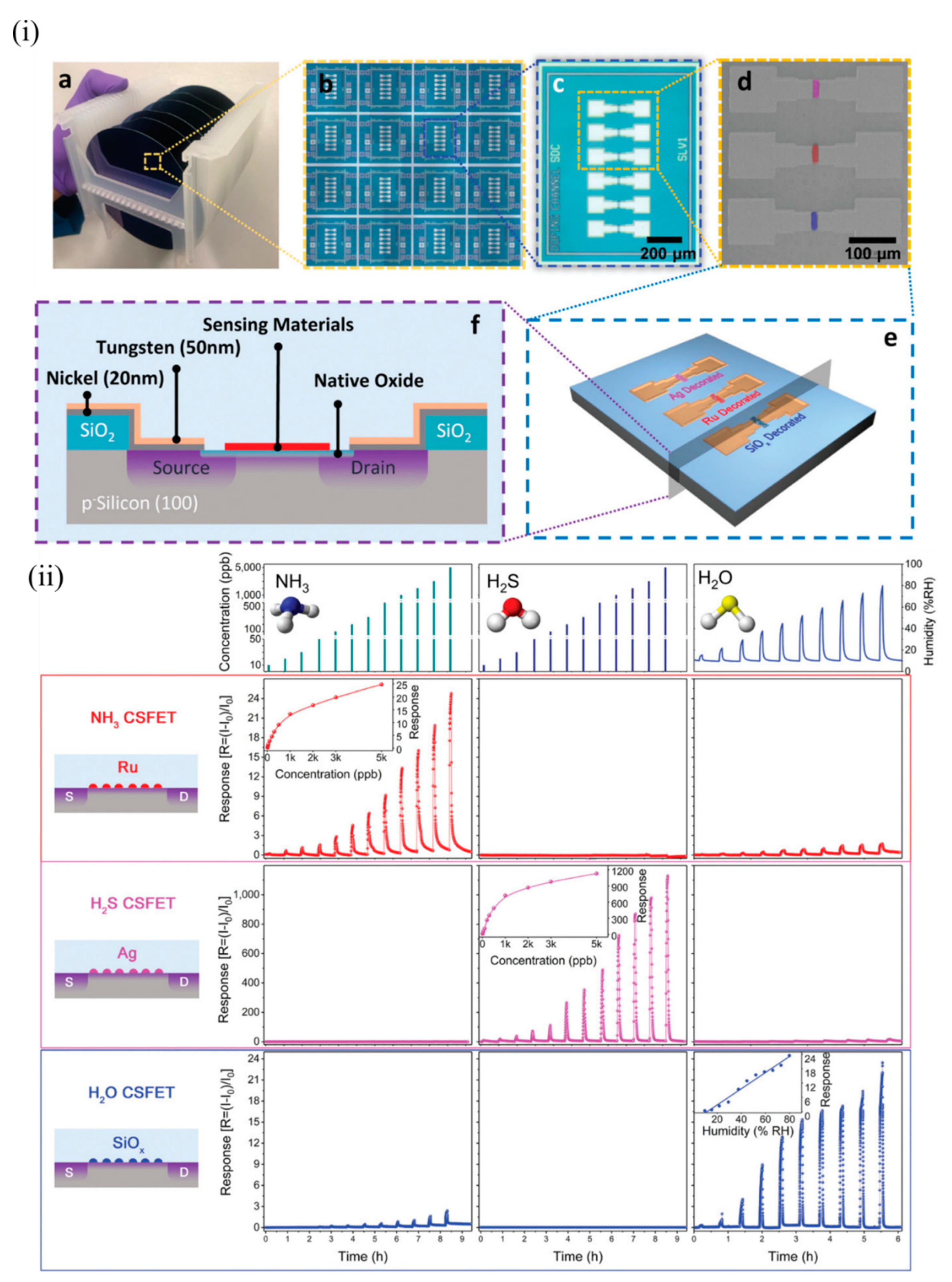 Figure 4. The multi-CS-FET array. (i) Device structure of CS-FETs: (a) photograph of 4 in wafers from which CS-FET arrays were fabricated, and (b) a magnified image of multiple arrays on a single wafer; (c) optical microscope image of a multimaterial-decorated CS-FET array, and (d) a corresponding SEM image with the location of different sensing materials marked in false color; (e) 3D schematic of the multi-CS-FET array, and (f) cross-sectional schematic of the device. (ii) Sensing performance of various NP-decorated CS-FETs. Response of each CS-FET towards different gases with varying concentration (at VDS = 1 V, Vsub = 0 V). Each row in the same color depicts the response curves of the CS-FET indicated on the left (NH3, H2S, and H2O CS-FET, from top to bottom). Each column indicates the response curves towards varying concentrations of the gas indicated at the top (NH3, H2S, and humidity, from left to right). Reproduced with permission from [35][53]. Copyright (2020) WILEY-VCH.
4. EFN FET Devices for Gas Sensing
Another class of Si-channel-based FET gas sensors are the SOI-based EFN gas sensors, which utilise multigate sensing technology. As the name suggests, the NW-like conducting channel in these sensors is not created physically, but by electrostatic control of the conduction channel through appropriate biasing of various junction and back gates, as will be explained below. The EFN gas sensor was first introduced as a specific, real-time, label-free biosensor for detection of protein–protein interactions at femtomolar concentrations [40][58]. The schematic of an n-type accumulation-type EFN device is shown in Figure 9 i. As depicted, the n-doped conducting channel forms two back-to-back junctions with two p + -doped regions on its sides that serve as junction gates. The p-type substrate below the buried oxide layer (BOX) forms the back gate. The EFN gas sensor resembles the G 4 field-effect transistor developed in 2002 [41][42][43][59,60,61], with the exception that the top metal gate is replaced by the top molecular gate provided by the target analyte molecules [44][27]. A negative bias on the back gate ( V BG ) depletes the SOI of majority carriers (electrons), and the accumulated channel is confined to the top of the SOI ( Figure 5 ii). Thus, the “height” of the channel is determined by the back gate potential in the bulk SOI. A negative bias on the junction gates ( V JG ) operates the p+-n junctions in reverse mode, thus increasing the depletion regions on both sides of the metallurgical junctions. A higher reverse bias on both sides will eventually create larger depletion regions and confine the conducting channel to narrower dimensions (also see Figure 5 ii). Thus, the width of the channel in the bulk SOI is predominantly controlled by the applied junction gate voltages. Figure 5 iii depicts an elongated channel with V BG = 0 V and negative V JG s. Thus, appropriate biasing of the various gate voltages allow tuning of the width and height, and hence the shape of the conducting channel. An application of an asymmetric bias to the V JG s ( V JG1 not equal to V JG2 ) controls the lateral position of the conducting channel (see Figure 5 iv, where V JG1 is not equal to V JG2 , and V BG is negative). An equal bias on the two junction gates ( V JG1 = V JG2 ) will position the EFN in the middle. A gradient of dopant concentration will also allow the EFN channel to be located in the middle and the bottom of the bulk SOI, such that concentrations are maximised in the middle and bottom of the SOI, respectively (see Figure 5 v,vi, respectively). However, it should be noted that reverse biasing of the p-n junctions is limited by the junction breakdown voltage determined by the dopant concentration (donors) of the bulk SOI. A smaller dopant concentration will enable a higher reverse bias, but can result in the absence of carriers for the formation of the channel.
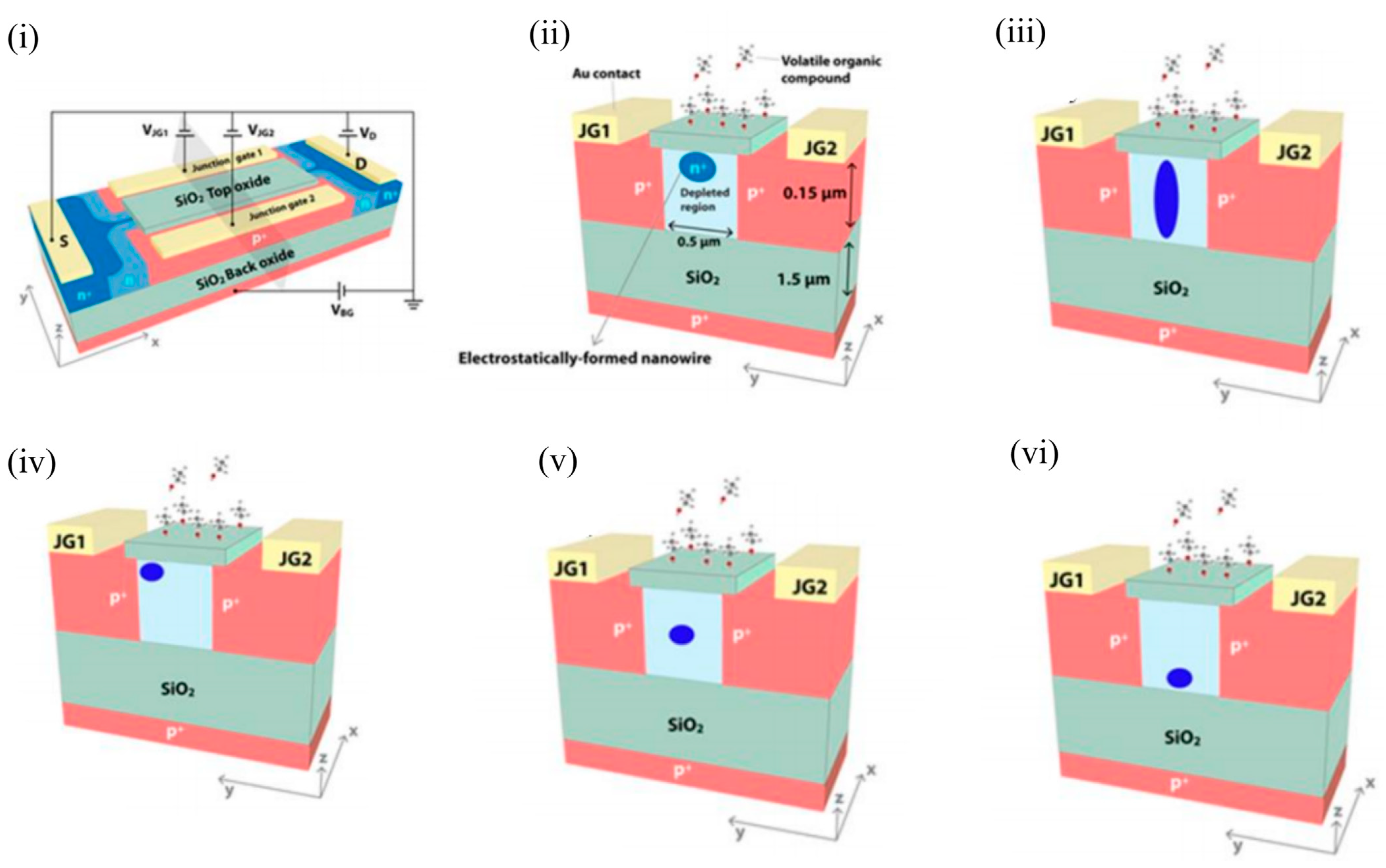 Figure 5. Design and various modes of operation of an EFN gas sensor. (i) EFN gas sensor in an electrical biasing configuration. (ii) Small EFN at the top of the bulk SOI: VJG1 = VJG2 < 0 V and VBG < 0 V. (iii) Elongated EFN: VJG1 = VJG2 < 0 V and VBG = 0 V. (iv) Asymmetric biasing configuration—small EFN near to JG1: VJG1 = 0 V, VJG2 < 0 V, and VBG < 0 V. (v) Small EFN in the middle: VJG1 = VJG2 < 0 V and VBG = 0 V. A gradient of donor concentration with a peak at the center of the SOI is required to position the EFN in the middle of the bulk SOI. (vi) Small EFN at the bottom: VJG1 = VJG2 < 0 V and VBG = 0 V. A gradient of donor concentration with a peak at the bottom of the SOI is required to position the EFN in the bottom of the bulk SOI. (i) and (ii) are reprinted from [45][62], with permission of Tsinghua University Press and Springer-Verlag Berlin Heidelberg, 2015. (iii–vi) are reprinted from [44][27] with permission to use under the Creative Commons license.
As can be observed in Figure 6 , a smaller EFN corresponding to more negative V JG and V BG was highly sensitive to lower concentrations, and saturation in response occurred early, thus contributing to a lower dynamic range. On the contrary, a wider EFN corresponding to a less negative V JG and V BG had a higher detection limit (estimated from the signal-to-noise ratio); the sensor response varied linearly even in the higher concentration regime, and had a higher upper threshold of concentration detection. It should be noted that surface potential changed rapidly with a small change in V JG ; however, the influence of the V BG change was not very much. Thus, the shape and size of the EFN nanowire was controlled electrostatically, which resulted in tunable sensor response and large dynamic range using a single device [46][67].
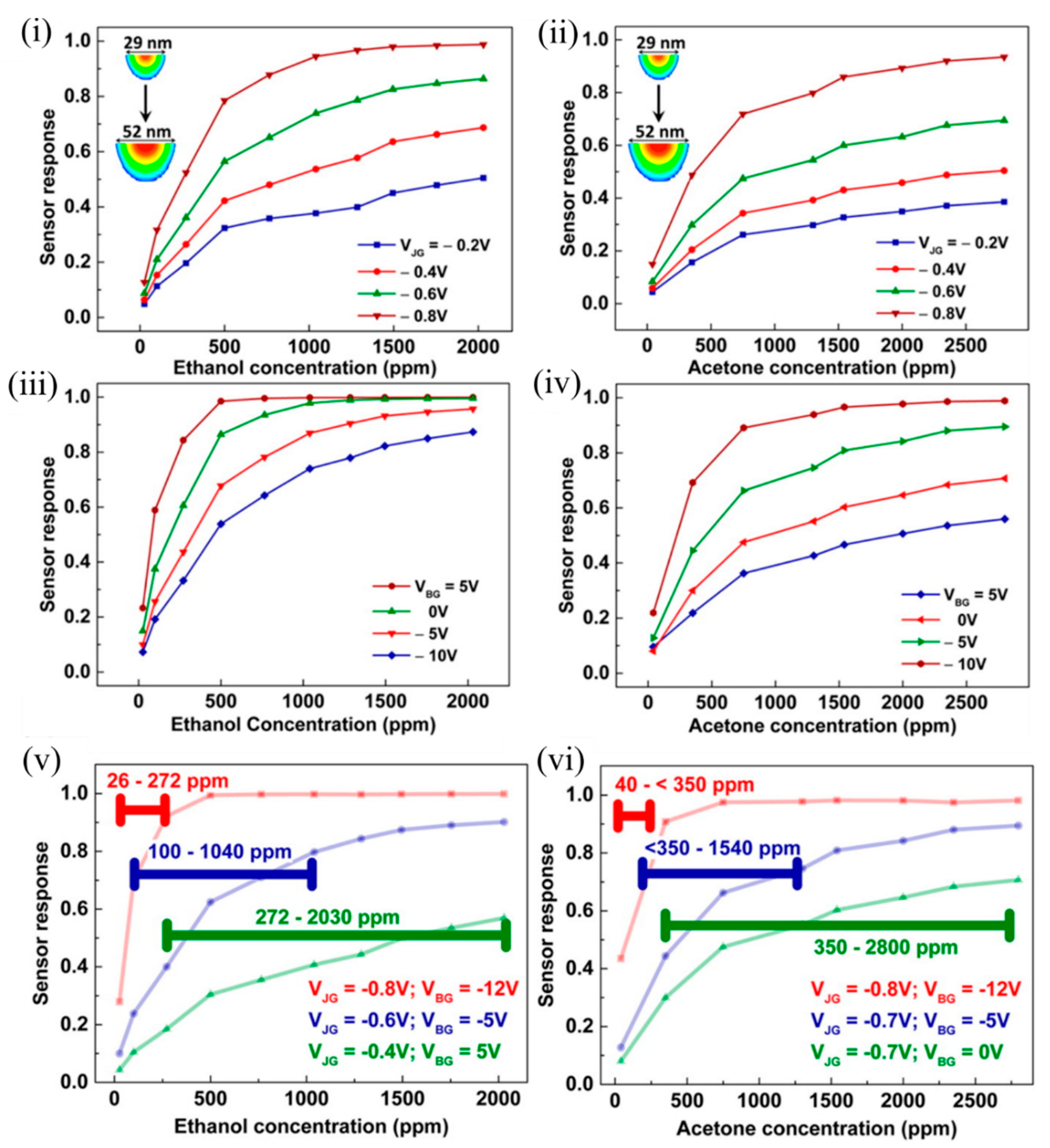 Figure 6. Sensor responses of the EFN to varying concentrations of ethanol and acetone. Sensor response as a function of VOC concentration measured at (i,ii) different VJG values at VBG = −3 V and (iii,iv) different VBG values at VJG = −0.7 V, for ethanol and acetone, respectively. Sensor response of the EFN device operated at different optimum gate biases to span the proposed dynamic range of (v) ~26–2030 ppm for ethanol, and (vi) ~40–2800 ppm for acetone. The horizontal lines indicate the calculated dynamic range for the particular EFN configuration such that the sensor response was ≥0.2 throughout. Reprinted with permission from [46][67]. Copyright (2016) American Chemical Society.
Several potential influencing factors were determined by the authors that might contribute to the sensing mechanism, such as interaction of molecules with the EFN SiO 2 surface, intermolecular interaction strength (and other molecular properties) and the surface-induced electric field on the EFN surface [47][70]. The dipole moments of the various tested alcohols varied (1.55–1.69 D) compared to the nonpolar alkanes, which contributed to the relatively weak sensor responses of the alkanes at equivalent concentrations. However, the dipole moments of the tested alcohols being largely similar could not solely explain the increased response due to the increasing chain length. The authors attributed this to the increased probability for intermolecular interactions arising due to more potential interaction sites due to more CHx groups on longer alkyl chain lengths. This contributed to a more compact, ordered and stabilised adsorption layer on the EFN surface, resulting in enhanced surface coverage [48][71]. Similar to alkanes, with increasing alkane chain length, adsorption energy increases, and an increased tendency to layer formation occurs, contributing to a more ordered and strongly interacting multilayer alkane structure on the EFN surface with better surface coverage. It also is shown in Figure 7 iii that a fringing electric field was induced by the p + -n regions on the EFN surface, which might also have played a crucial role in the sensing. As the reverse bias on the junction gates was increased on either side of the channel, it increased the induced electric field in the space charge region. This induced electric field was of the order of 10 6 V/cm for the applied junction gate bias in the range of 0–2 V. As observed in Figure 7 iv, as the negative bias on the junction gate was increased, the sensor response also increased. A narrow channel corresponding to a more negative junction gate also was a contributing factor to the increased sensor response, as a small channel was more sensitive to minute changes in surface potential induced by the adsorption of analytes. In addition, this surface electric field might contribute to induced dipole moments in the polarizable alkane molecules, which can contribute to their sensor response at higher concentrations. In addition, polarizability of molecules is known to increase with molecule size, and decreased vapour pressure due to an increase in chain length. This might be another contributing factor to increased sensor response with higher alkanes. Thus, the authors offered a very good discussion of several contributing factors for the sensing mechanism [47][70].
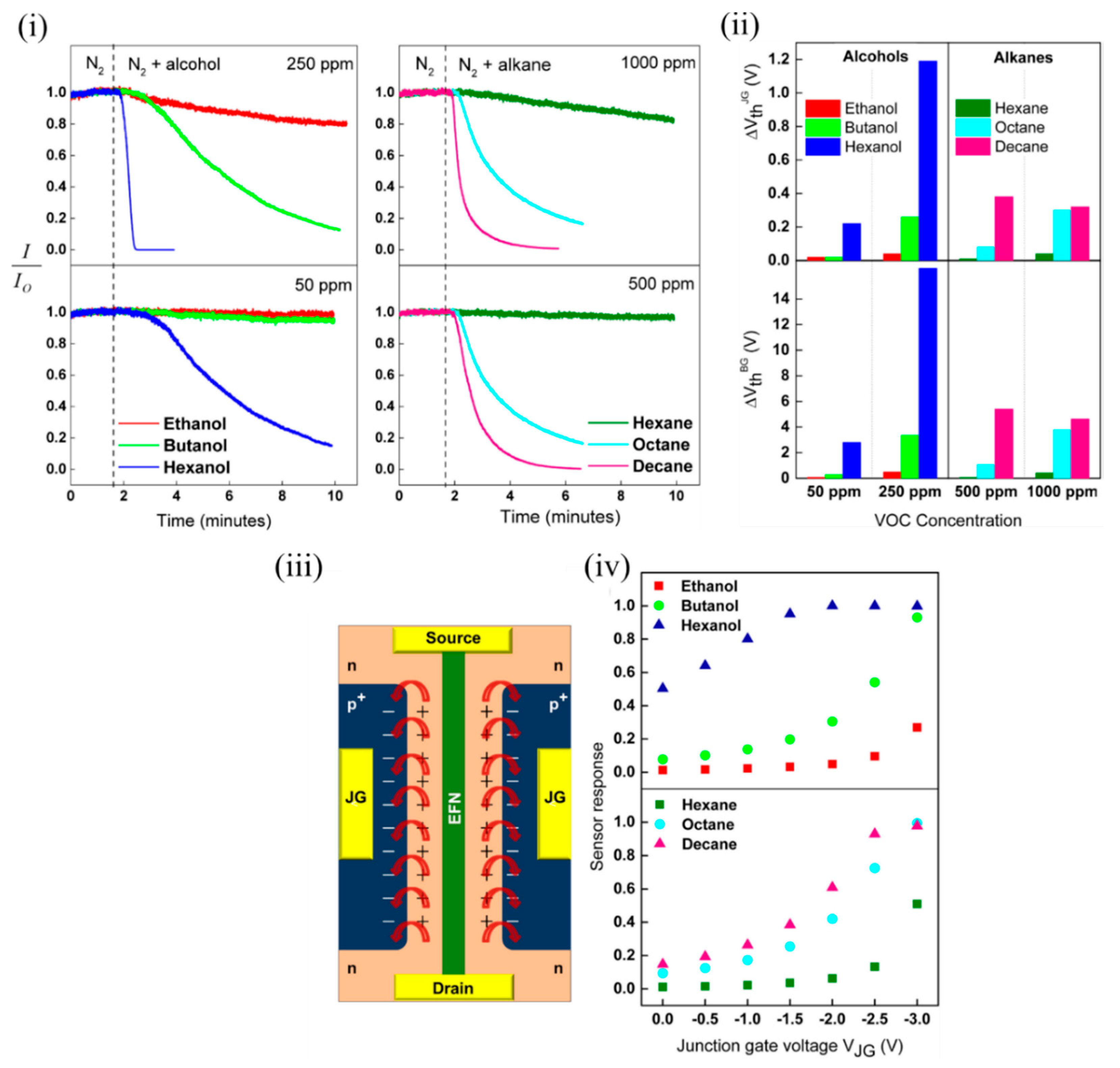 Figure 7. EFN sensor for sensing polar alcohols and nonpolar alkanes. (i) Plot of normalized sensor response of the EFN vs. time for alcohols (left) and alkanes (right). (ii) Plot of shift in threshold voltage of the EFN sensor with respect to the junction gate (top) and back gate (below) at two different concentrations of alcohols (50 and 250 ppm) (left) and alkanes (500 and 1000 ppm) (right). (iii) Schematic top view of the EFN sensor depicting the two back-to-back p-n regions on either side of the channel marked with ‘+’ and ‘−’ (the top oxide is not shown for clarity). The red arrows indicate the fringing fields due to the induced electric fields in the space charge region. (iv) Plot of sensor response to alcohols (top) and alkanes (bottom) vs. the applied junction gate voltage of the EFN. Adapted and reprinted with permission from [47][70]. Copyright (2017) Elsevier.
The authors simulated the fringing field strength to be in the range of 0.5 × 10 5 to 2.5 × 10 5 V/cm when the junction gate bias was varied from 0.5 to −2.5 V. Beyond 0.5 V, significant p-n junction diffusion leakage currents arose, which marked the upper threshold limit. Below −2 V, the n-Si channel was fully depleted of electrons and marked the lower threshold limit. As seen in Figure 8 i,ii, the electric field in the case of negative junction gate penetrated into the ambient at the top of the dielectric and could influence the adsorption of VOC analytes. It should be mentioned that a change in doping profile of the n channel would allow a different range of junction gate biases. The fringing field was strongest above the p-n junction and then decreased exponentially in the ambient. Figure 8 iii depicts the shift in back gate threshold voltages due to ethanol exposure at specific positive and negative junction gates. Figure 8 iv shows the sensor response of the EFN to 2000 ppm of ethanol at various junction gates. The sensor response correlated with the simulated fringing field strength (red). Figure 8 v depicts the EFN sensor responses to equal concentrations of ethanol (top) and n-butylamine (below). Figure 8 vi depicts how the surface electric field could selectively detect ethanol and butylamine. A suitable choice of the working point ( V JG = 0.2 V and V D = 0.4 V) facilitated discrimination between the molecules ( Figure 8 vi, solid lines). Thus, efficient tuning of the intrinsic sensor response is shown, with the variation of the fringing field strength controlled by the applied junction gate biases.
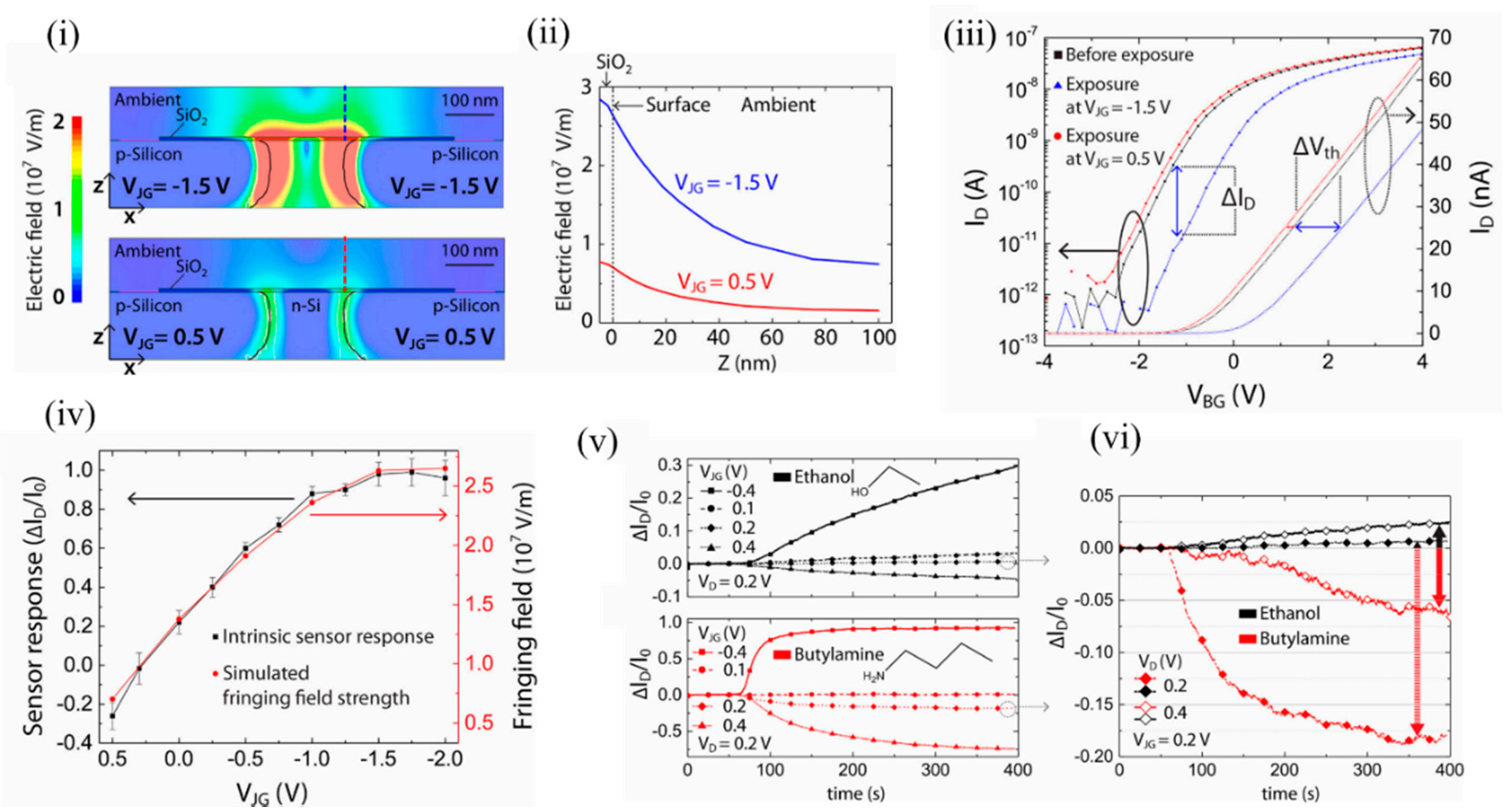 Figure 8. Induced fringing electric field on the surface of the EFN as a tool for selectivity between VOCs. (i) The electric field distributions at the cross sections (x–z planes) of the 3D-modeled EFN device at VJG = −1.5 V (top) and VJG = 0.5 V (bottom) with other electrodes as grounded. (ii) Decaying of the simulated electric field strength with the distance from the sensor surface (Z-axis) above the p–n junction of the EFN device, indicated by the dashed lines in (i). (iii) ID–VBG characteristics in nitrogen before ethanol exposure (black) and after ethanol exposure at VJG = −1.5 V (blue), and VJG = 0.5 V (red) after saturation in sensing had been reached. (iv) Plots of the sensor response: ΔID/I0, (black) and the simulated fringing field maxima (red) as a function of VJG. (v) Plot of sensor response vs. time for exposure to 1500 ppm concentrations of ethanol (top) and n-butylamine (bottom) vapors at four different VJGs, and at constant VD = 0.2 V and VBG = −20 V. (vi) Comparison of the sensor responses between ethanol and n-butylamine at VD = 0.2 V and VD = 0.4 V, at constant VJG = 0.2 V and VBG = −20 V, indicating selectivity at definite working voltages. Reprinted with permission from [49][72]. Copyright (2018) American Chemical Society.