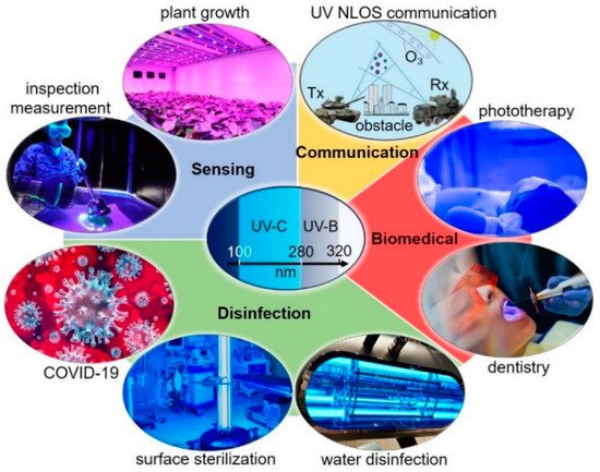
The development of electrically pumped semiconductor diode lasers emitting at the ultraviolet (UV)-B and -C spectral bands has been an active area of research over the past several years, motivated by a wide range of emerging applications. III-Nitride materials and their alloys, in particular AlGaN, are the material of choice for the development of this ultrashort-wavelength laser technology. Despite significant progress in AlGaN-based light-emitting diodes (LEDs), the technological advancement and innovation in diode lasers at these spectral bands is lagging due to several technical challenges.
- AlGaN
- electrically-pumped
- UV-B and -C
- p-doping
- thin films
- nanowires
- hole injection
- quantum wells
1. Introduction
2. Overview of Recent Progress of AlGaN Ultraviolet (UV)-B and -C Lasers
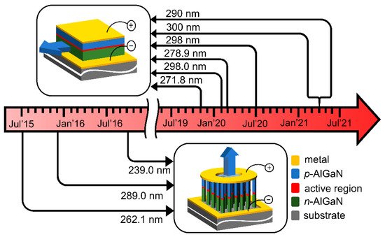
| Reference | Growth Method | Material Type | Lasing Wavelength (nm) | Threshold (kA/cm | 2 | ) | Substrate | Operating Temp. |
Operating Mode |
|---|
| Zhang et al., 2019 [30] | Zhang et al., 2019 [23] | MOCVD | Thin film | 271.8 | 25 | AlN single crystal | RT | Pulse |
| Sato et al., 2020 [31] | Sato et al., 2020 [24] | MOCVD | Thin film | 298 | 41 | AlN/sapphire | RT | Pulse |
| Sakai et al., 2020 [33] | Sakai et al., 2020 [25] | MOCVD | Thin film | 278.9 | 19.6 | AlN single crystal | RT | Pulse |
| Omori et al., 2020 [32] | Omori et al., 2020 [26] | MOCVD | Thin film | 298 | 25 | AlN/sapphire | RT | Pulse |
| Kushimoto et al., 2021 [34] | Kushimoto et al., 2021 [30] | MOCVD | Thin film | 271.2 | AlN single crystal | RT | Pulse | |
| Tanaka et al., 2021 [35] | Tanaka et al., 2021 [31] | MOCVD | Thin film | 300 | 13.3 | AlN/sapphire | RT | Pulse |
| Tanaka et al., 2021 [36] | Tanaka et al., 2021 [32] | MOCVD | Thin film | 290 | 35 | AlN/sapphire | RT | Pulse |
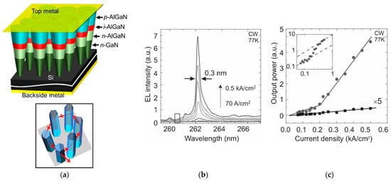
| Zhao et al., 2015 [28] | MBE | Nanowire | 262.1 | 0.2 | Si | 77K | CW | |
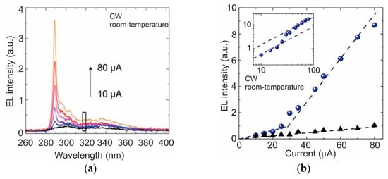
| Zhao et al., 2015 [27] | MBE | Nanowire | 289 | 0.3 | Si | RT | CW | |
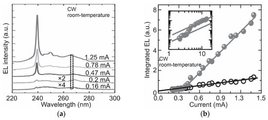
| Zhao et al., 2016 [29] | MBE | Nanowire | 239 | Si | RT | CW |
3. Challenges of AlGaN UV-B/C Lasers
3.1. Substrates and Defects
3.2. P- and N-Doping for High-Al
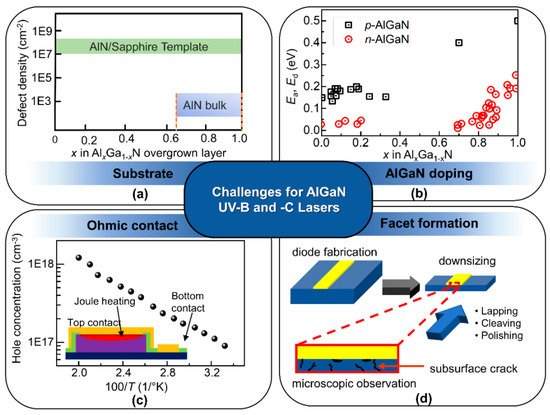
As UV-B and -C lasers require high-quality, low-defect and thick AlGaN cladding layers for improved waveguiding [24[49][50],85], their electrical performance is equally important. To achieve the high current density required in the active regions for laser operation, cladding layers need to be conductive which is particularly challenging for p-type doping for all x of AlxGa1−xN, as shown in Figure 3b [72][36]. Behind ineffective p-doping, the most formidable challenges include large acceptor ionization energy for Mg dopants in AlGaN [86[51][52],87], formation of low energies by compensating defects (donors) like nitrogen vacancies [88][53], limitation of solubility of Mg in AlGaN [71[35][54],89], hydrogen passivation of the Mg dopants [70,90][34][55] and the existence of parasitic impurities, such as hydrogen (H), carbon (C) and oxygen (O) [69,91,92][33][56][57]. Compared to p-type doping, n-type doping is easily attainable and Si-doped AlGaN up to x = 0.8 with a reasonable doping concentration was achieved [73,74,75][37][38][39]. However, a sharp increase in resistance was observed due to the high activation energy of Si which increases exponentially from 25 meV–250 meV once the x > 0.8 for n-AlxGa1−xN [73][37]. On top of this, the presence of compensating impurities carbon and oxygen in AlN substrates as well as MOCVD reactor impurities decrease donor concentrations in AlGaN with x > 0.85 by an order of magnitude [68,91,93][48][56][58].3.3. Low-Resistive Ohmic Contact
Figure 3c shows the representative AlGaN lasers with co-planar or intracavity contacts, which is the only possible way to form bottom n-side contacts. As the improvement in n- and p-type conductivity in Al-rich AlGaN continues, the low resistive ohmic contact realization emerges.3.4. Facet Formation
4. Critical Technical Areas for AlGaN UV-B and -C Lasers
Figure 4 schematically shows the four major technical pillars that will determine the success of UV-B and -C laser technology and underpin the implementation of high-performance AlGaN devices.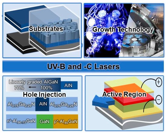
4.1. Substrate Materials
Figure 5 schematically shows all the possible substrates that are used for implementing EP AlGaN lasers.

4.2. Growth Technology
The two most popular methods available for epitaxial growth AlGaN UV laser materials are molecular beam epitaxy (MBE) [128,131,132,133][61][62][63][64] and metalorganic chemical vapor deposition (MOCVD) [134,135,136][65][66][67]. When it comes to templated substrates, MOCVD is superior to MBE for growing high-quality AlN templates due to high growth-temperatures and -rates [137,138,139][68][69][70].
Although not as extensive as MOCVD, MBE-grown UV materials, i.e., both thin film and NWs, have also been studied over the years. As a matter of fact, MBE offers some distinct benefits over MOCVD in terms of interface diffusion, defect control, memory effect, high hole concentration in p-AlGaN, Mg passivation and significant control over defect incorporation [143][71]. Due to its relatively low growth temperature MBE grown samples do not suffer from surface damage due to chemical reaction at high temperature often associated with MOCVD. This suggests the superiority of MBE over MOCVD in terms of growing high-quality active regions.
Lasers with buried TJ may require a hybrid MOCVD/MBE growth approach [147,148][72][73]. In such structures, a base structure, containing all the layers up to an active region and the p+-side of the TJ, is grown by MOCVD, and the remainder of the device including the n+-side of TJs, n-cladding and n+-contact layers can be overgrown during the second epitaxial growth by MBE. Hence, the hybrid approach, comprising a MOCVD-grown base structure with the active region and MBE-grown TJs, is another viable alternative towards obtaining high-performance UV-B and -C lasers.
4.3. Three Major Techniques for Hole Injection
4.3.1. Distributed Polarization Doping
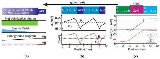
Introducing dopants in AlGaN by compositionally grading, commonly addressed as DPD takes advantage of both spontaneous and piezoelectric polarization. Since its first demonstration, DPD has been widely popular as an effective means to enhance p-AlGaN doping [153][74].Figure 6a shows how compositionally graded AlGaN creates polarization-induced 3D charges that result in free carriers.
4.3.2. Short-Period Superlattice
A short-period superlattice, comprising of alternate layers of AlxGa1−xN with high and low x doped with Mg (AlxGa1−xN/AlyGa1−yN with x > y) was used to improve hole activation with the help of band offset and strong built-in spontaneous and piezoelectric polarization fields instead of thermal energy [158,159,160,161][75][76][77][78]. By improving vertical conductivity, the resistance of an SPSL reduced nearly 12 times compared to a bulk layer with the same composition, making the SPSL layer suitable to operate at a high voltage [56][17].
4.3.3. Tunnel Junctions (TJs)
With the help of polarization doping, successful demonstration of GaN-based TJ was reported since 2001 [162][79] and in 2016 the first AlGaN based TJ was reported [163][80]. While p-AlGaN is necessary for p-side cladding, implementing a TJ eliminates the thick p-cladding layer requirement. The use of TJs as an intracavity contact for hole injection through interband tunneling is reported in a number of experimental studies [55,150,151,164,165][16][81][82][83][84].
4.4. Active Region
For the successful design and demonstrations of UV-B and -C lasers, one primarily requires a good AlGaN-based active region to obtain high material gain [22,53,154][85][13][86]. This includes not only a good material quality with low-defects and sharp interfaces but also an optimal number of QWs, and the right thicknesses of QWs and barrier with optimal band offsets and adjusting the waveguide thickness [16,167,168][87][88][89]. These considerations will be added by the polarization switching phenomena of emitted light for the unique AlGaN material system [169,170][90][91]. Using a higher number of QWs appears to be non-conventional in the wavelengths of interest due to the constraint of uniform pumping of all the QWs with carriers to obtain material gain. If one of the quantum wells cannot be pumped enough, they will operate as a band-edge absorbing layer and then it fails to lase.
5. Demonstration of AlGaN Lasers
5.1. Thin Film Lasers
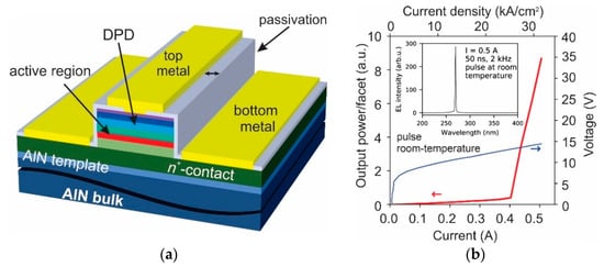
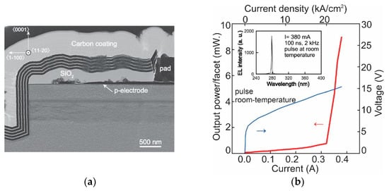
In 2019, the first thin film-based EP AlGaN laser at UV-C was achieved by researchers at Nagoya University, Japan, in cooperation with Asahi Kasei Corporation, Chiyoda City, Japan and Crystal IS, Inc., Green Island, NY, USA [30]. The laser materials were pseudomorphically grown on (0001) bulk AlN substrates by MOCVD. The devices used a single AlGaN 9-nm-thick QW to emit at 271.8 nm. For hole injection, pseudomorphic DPD layers were used on top of
In 2019, the first thin film-based EP AlGaN laser at UV-C was achieved by researchers at Nagoya University, Japan, in cooperation with Asahi Kasei Corporation, Chiyoda City, Japan and Crystal IS, Inc., Green Island, NY, USA [23]. The laser materials were pseudomorphically grown on (0001) bulk AlN substrates by MOCVD. The devices used a single AlGaN 9-nm-thick QW to emit at 271.8 nm. For hole injection, pseudomorphic DPD layers were used on top of
p
-waveguide.
Figure 7
a schematically shows the fully processed FP lasers.
5.2. Nanowire Lasers
References
- Majumdar, A.K. Non-line-of-sight (NLOS) ultraviolet and indoor free-space optical (FSO) communications. In Advanced Free Space Optics (FSO); Springer: Berlin/Heidelberg, Germany, 2015; pp. 177–202.
- Reilly, D.M.; Moriarty, D.T.; Maynard, J.A. Unique properties of solar blind ultraviolet communication systems for unattended ground sensor networks. In Proceedings of the Unmanned/Unattended Sensors and Sensor Networks, London, UK, 1 September 2004; pp. 244–254.
- Bhar, G.; Chatterjee, U. Development of ultraviolet laser for disinfection of potable water. Indian J. Phys. 2006, 80, 517–521.
- Vilhunen, S.; Särkkä, H.; Sillanpää, M. Ultraviolet light-emitting diodes in water disinfection. Environ. Sci. Pollut. Res. 2009, 16, 439–442.
- Grishkanich, A.; Zhevlakov, A.; Kascheev, S.; Polyakov, V.; Sidorov, I.; Ruzankina, J.; Yakovlev, A.; Mak, A. Study methods for disinfection water for injection. In Proceedings of the Biophotonics: Photonic Solutions for Better Health Care V, Brussels, Belgium, 4–7 April 2016; p. 98873K.
- Nelson, J.S.; Berns, M.W. Laser applications in biomedicine. Part II: Clinical applications. J. Laser Appl. 1989, 1, 9–20.
- Letokhov, V.S. Laser light in biomedicine and the life sciences: From the present to the future. In Biomedical Photonics Handbook; CRC Press: Boca Raton, FL, USA, 2003; pp. 177–192.
- Raeiszadeh, M.; Adeli, B. A Critical Review on Ultraviolet Disinfection Systems against COVID-19 Outbreak: Applicability, Validation, and Safety Considerations. ACS Photon. 2020, 7, 2941–2951.
- Gerchman, Y.; Mamane, H.; Friedman, N.; Mandelboim, M. UV-LED disinfection of Coronavirus: Wavelength effect. J. Photochem. Photobiol. B Biol. 2020, 212, 112044.
- Armstrong, A.; Allerman, A.A.; Fischer, A.J.; King, M.P.; Van Heukelom, M.; Moseley, M.W.; Kaplar, R.; Wierer, J.; Crawford, M.H.; Dickerson, J.R. Ultra-Wide Bandgap AlGaN Materials for Electronics and Opto-Electronics; Sandia National Lab. (SNL-NM): Albuquerque, NM, USA, 2016.
- Electronics, B. UV Light Emitting DIodes (UV A/B/C LEDs). Available online: (accessed on 7 July 2021).
- Lumileds. LUXEON UV LEDs. Available online: (accessed on 7 July 2021).
- Zhang, Z.; Kushimoto, M.; Sakai, T.; Sugiyama, N.; Schowalter, L.J.; Sasaoka, C.; Amano, H. Design and characterization of a low-optical-loss UV-C laser diode. Jpn. J. Appl. Phys. 2020, 59, 094001.
- Guo, Q.; Kirste, R.; Mita, S.; Tweedie, J.; Reddy, P.; Moody, B.; Guan, Y.; Washiyama, S.; Klump, A.; Sitar, Z. Design of AlGaN-based quantum structures for low threshold UVC lasers. J. Appl. Phys. 2019, 126, 223101.
- Kawase, Y.; Ikeda, S.; Sakuragi, Y.; Yasue, S.; Iwayama, S.; Iwaya, M.; Takeuchi, T.; Kamiyama, S.; Akasaki, I.; Miyake, H. Ultraviolet-B band lasers fabricated on highly relaxed thick Al0. 55Ga0. 45N films grown on various types of AlN wafers. Jpn. J. Appl. Phys. 2019, 58, SC1052.
- Zhang, Y.; Krishnamoorthy, S.; Akyol, F.; Allerman, A.A.; Moseley, M.W.; Armstrong, A.M.; Rajan, S. Design of p-type cladding layers for tunnel-injected UV-A light emitting diodes. Appl. Phys. Lett. 2016, 109, 191105.
- Martens, M.; Kuhn, C.; Ziffer, E.; Simoneit, T.; Kueller, V.; Knauer, A.; Rass, J.; Wernicke, T.; Einfeldt, S.; Weyers, M. Low absorption loss p-AlGaN superlattice cladding layer for current-injection deep ultraviolet laser diodes. Appl. Phys. Lett. 2016, 108, 151108.
- Mueller, S.G.; Bondokov, R.T.; Morgan, K.E.; Slack, G.A.; Schujman, S.B.; Grandusky, J.; Smart, J.A.; Schowalter, L.J. The progress of AlN bulk growth and epitaxy for electronic applications. Phys. Status Solidi (A) 2009, 206, 1153–1159.
- Bryan, Z.; Bryan, I.; Xie, J.; Mita, S.; Sitar, Z.; Collazo, R. High internal quantum efficiency in AlGaN multiple quantum wells grown on bulk AlN substrates. Appl. Phys. Lett. 2015, 106, 142107.
- Grandusky, J.R.; Chen, J.; Gibb, S.R.; Mendrick, M.C.; Moe, C.G.; Rodak, L.; Garrett, G.A.; Wraback, M.; Schowalter, L.J. 270 nm pseudomorphic ultraviolet light-emitting diodes with over 60 mW continuous wave output power. Appl. Phys. Express 2013, 6, 032101.
- Yoshida, H.; Yamashita, Y.; Kuwabara, M.; Kan, H. Demonstration of an ultraviolet 336 nm AlGaN multiple-quantum-well laser diode. Appl. Phys. Lett. 2008, 93, 241106.
- Li, K.; Liu, X.; Wang, Q.; Zhao, S.; Mi, Z. Ultralow-threshold electrically injected AlGaN nanowire ultraviolet lasers on Si operating at low temperature. Nat. Nanotechnol. 2015, 10, 140.
- Zhang, Z.; Kushimoto, M.; Sakai, T.; Sugiyama, N.; Schowalter, L.J.; Sasaoka, C.; Amano, H. A 271.8 nm deep-ultraviolet laser diode for room temperature operation. Appl. Phys. Express 2019, 12, 124003.
- Sato, K.; Yasue, S.; Yamada, K.; Tanaka, S.; Omori, T.; Ishizuka, S.; Teramura, S.; Ogino, Y.; Iwayama, S.; Miyake, H. Room-temperature operation of AlGaN ultraviolet-B laser diode at 298 nm on lattice-relaxed Al0. 6Ga0. 4N/AlN/sapphire. Appl. Phys. Express 2020, 13, 031004.
- Sakai, T.; Kushimoto, M.; Zhang, Z.; Sugiyama, N.; Schowalter, L.J.; Honda, Y.; Sasaoka, C.; Amano, H. On-wafer fabrication of etched-mirror UV-C laser diodes with the ALD-deposited DBR. Appl. Phys. Lett. 2020, 116, 122101.
- Omori, T.; Ishizuka, S.; Tanaka, S.; Yasue, S.; Sato, K.; Ogino, Y.; Teramura, S.; Yamada, K.; Iwayama, S.; Miyake, H. Internal loss of AlGaN-based ultraviolet-B band laser diodes with p-type AlGaN cladding layer using polarization doping. Appl. Phys. Express 2020, 13, 071008.
- Zhao, S.; Woo, S.; Bugnet, M.; Liu, X.; Kang, J.; Botton, G.; Mi, Z. Three-dimensional quantum confinement of charge carriers in self-organized AlGaN nanowires: A viable route to electrically injected deep ultraviolet lasers. Nano Lett. 2015, 15, 7801–7807.
- Zhao, S.; Liu, X.; Woo, S.; Kang, J.; Botton, G.; Mi, Z. An electrically injected AlGaN nanowire laser operating in the ultraviolet-C band. Appl. Phys. Lett. 2015, 107, 043101.
- Zhao, S.; Liu, X.; Wu, Y.; Mi, Z. An electrically pumped 239 nm AlGaN nanowire laser operating at room temperature. Appl. Phys. Lett. 2016, 109, 191106.
- Kushimoto, M.; Zhang, Z.; Sugiyama, N.; HONDA, Y.; Schowalter, L.J.; Sasaoka, C.; Amano, H. Impact of heat treatment process on threshold current density in AlGaN-based deep-ultraviolet laser diodes on AlN substrate. Appl. Phys. Express 2021, 14, 051003.
- Tanaka, S.; Ogino, Y.; Yamada, K.; Omori, T.; Ogura, R.; Teramura, S.; Shimokawa, M.; Ishizuka, S.; Yabutani, A.; Iwayama, S. AlGaN-based UV-B laser diode with a high optical confinement factor. Appl. Phys. Lett. 2021, 118, 163504.
- Tanaka, S.; Teramura, S.; Shimokawa, M.; Yamada, K.; Omori, T.; Iwayama, S.; Sato, K.; Miyake, H.; Iwaya, M.; Takeuchi, T. AlGaN-based UV-B laser diode with a wavelength of 290 nm on 1 μm periodic concavo–convex pattern AlN on a sapphire substrate. Appl. Phys. Express 2021, 14, 055505.
- Li, J.; Oder, T.; Nakarmi, M.; Lin, J.; Jiang, H. Optical and electrical properties of Mg-doped p-type AlxGa1−xN. Appl. Phys. Lett. 2002, 80, 1210–1212.
- Suzuki, M.; Nishio, J.; Onomura, M.; Hongo, C. Doping characteristics and electrical properties of Mg-doped AlGaN grown by atmospheric-pressure MOCVD. J. Cryst. Growth 1998, 189, 511–515.
- Jeon, S.-R.; Ren, Z.; Cui, G.; Su, J.; Gherasimova, M.; Han, J.; Cho, H.-K.; Zhou, L. Investigation of Mg doping in high-Al content p-type AlxGa1−xN (0.3 < x < 0.5). Appl. Phys. Lett. 2005, 86, 082107.
- Kinoshita, T.; Obata, T.; Yanagi, H.; Inoue, S.-i. High p-type conduction in high-Al content Mg-doped AlGaN. Appl. Phys. Lett. 2013, 102, 012105.
- Borisov, B.; Kuryatkov, V.; Kudryavtsev, Y.; Asomoza, R.; Nikishin, S.; Song, D.; Holtz, M.; Temkin, H. Si-doped AlxGa1−xN (0.56 ≤ x ≤ 1) layers grown by molecular beam epitaxy with ammonia. Appl. Phys. Lett. 2005, 87, 132106.
- Mehnke, F.; Wernicke, T.; Pingel, H.; Kuhn, C.; Reich, C.; Kueller, V.; Knauer, A.; Lapeyrade, M.; Weyers, M.; Kneissl, M. Highly conductive n-Al x Ga1− x N layers with aluminum mole fractions above 80%. Appl. Phys. Lett. 2013, 103, 212109.
- Taniyasu, Y.; Kasu, M.; Kobayashi, N. Intentional control of n-type conduction for Si-doped AlN and AlxGa1−xN (0.42 ≤ x < 1). Appl. Phys. Lett. 2002, 81, 1255–1257.
- Katsuragawa, M.; Sota, S.; Komori, M.; Anbe, C.; Takeuchi, T.; Sakai, H.; Amano, H.; Akasaki, I. Thermal ionization energy of Si and Mg in AlGaN. J. Cryst. Growth 1998, 189, 528–531.
- Hirayama, H.; Maeda, N.; Fujikawa, S.; Toyoda, S.; Kamata, N. Recent progress and future prospects of AlGaN-based high-efficiency deep-ultraviolet light-emitting diodes. Jpn. J. Appl. Phys. 2014, 53, 100209.
- Shatalov, M.; Sun, W.; Lunev, A.; Hu, X.; Dobrinsky, A.; Bilenko, Y.; Yang, J.; Shur, M.; Gaska, R.; Moe, C. AlGaN deep-ultraviolet light-emitting diodes with external quantum efficiency above 10%. Appl. Phys. Express 2012, 5, 082101.
- Ban, K.; Yamamoto, J.-i.; Takeda, K.; Ide, K.; Iwaya, M.; Takeuchi, T.; Kamiyama, S.; Akasaki, I.; Amano, H. Internal quantum efficiency of whole-composition-range AlGaN multiquantum wells. Appl. Phys. Express 2011, 4, 052101.
- Hirayama, H. Growth of High-Quality AlN on Sapphire and Development of AlGaN-Based Deep-Ultraviolet Light-Emitting Diodes. In Semiconductors and Semimetals; Elsevier: Amsterdam, The Netherlands, 2017; Volume 96, pp. 85–120.
- Hwang, S.; Morgan, D.; Kesler, A.; Lachab, M.; Zhang, B.; Heidari, A.; Nazir, H.; Ahmad, I.; Dion, J.; Fareed, Q. 276 nm substrate-free flip-chip AlGaN light-emitting diodes. Appl. Phys. Express 2011, 4, 032102.
- Susilo, N.; Hagedorn, S.; Jaeger, D.; Miyake, H.; Zeimer, U.; Reich, C.; Neuschulz, B.; Sulmoni, L.; Guttmann, M.; Mehnke, F. AlGaN-based deep UV LEDs grown on sputtered and high temperature annealed AlN/sapphire. Appl. Phys. Lett. 2018, 112, 041110.
- Kim, M.; Fujita, T.; Fukahori, S.; Inazu, T.; Pernot, C.; Nagasawa, Y.; Hirano, A.; Ippommatsu, M.; Iwaya, M.; Takeuchi, T. AlGaN-based deep ultraviolet light-emitting diodes fabricated on patterned sapphire substrates. Appl. Phys. Express 2011, 4, 092102.
- Hartmann, C.; Wollweber, J.; Sintonen, S.; Dittmar, A.; Kirste, L.; Kollowa, S.; Irmscher, K.; Bickermann, M. Preparation of deep UV transparent AlN substrates with high structural perfection for optoelectronic devices. Cryst. Eng. Comm. 2016, 18, 3488–3497.
- Kuhn, C.; Martens, M.; Mehnke, F.; Enslin, J.; Schneider, P.; Reich, C.; Krueger, F.; Rass, J.; Park, J.B.; Kueller, V. Influence of waveguide strain and surface morphology on AlGaN-based deep UV laser characteristics. J. Phys. D Appl. Phys. 2018, 51, 415101.
- Ponce, F.; Major, J., Jr.; Plano, W.; Welch, D. Crystalline structure of AlGaN epitaxy on sapphire using AlN buffer layers. Appl. Phys. Lett. 1994, 65, 2302–2304.
- Nam, K.; Nakarmi, M.; Li, J.; Lin, J.; Jiang, H. Mg acceptor level in AlN probed by deep ultraviolet photoluminescence. Appl. Phys. Lett. 2003, 83, 878–880.
- Abeles, B. Lattice Thermal Conductivity of Disordered Semiconductor Alloys at High Temperatures. Phys. Rev. 1963, 131, 1906–1911.
- Van de Walle, C.G.; Stampfl, C.; Neugebauer, J.; McCluskey, M.; Johnson, N. Doping of aigan alloys. MRS Online Proc. Libr. (OPL) 1998, 537.
- Chakraborty, A.; Moe, C.G.; Wu, Y.; Mates, T.; Keller, S.; Speck, J.S.; DenBaars, S.P.; Mishra, U.K. Electrical and structural characterization of Mg-doped p-type Al 0.69 Ga 0.31 N films on SiC substrate. J. Appl. Phys. 2007, 101, 053717.
- Zvanut, M.; Sunay, U.R.; Dashdorj, J.; Willoughby, W.; Allerman, A. Mg-hydrogen interaction in AlGaN alloys. In Gallium Nitride Materials and Devices VII; International Society for Optics and Photonics: Bellingham, WA, USA, 2012; p. 82620L.
- Lyons, J.; Janotti, A.; Van de Walle, C. Effects of carbon on the electrical and optical properties of InN, GaN, and AlN. Phys. Rev. B 2014, 89, 035204.
- Reshchikov, M.A.; Morkoç, H. Luminescence properties of defects in GaN. J. Appl. Phys. 2005, 97, 5–19.
- Gordon, L.; Lyons, J.; Janotti, A.; Van de Walle, C. Hybrid functional calculations of D X centers in AlN and GaN. Phys. Rev. B 2014, 89, 085204.
- Ni, R.; Chuo, C.-C.; Yang, K.; Ai, Y.; Zhang, L.; Cheng, Z.; Liu, Z.; Jia, L.; Zhang, Y. AlGaN-based ultraviolet light-emitting diode on high-temperature annealed sputtered AlN template. J. Alloys Compd. 2019, 794, 8–12.
- Hsu, Y.; Chang, S.-J.; Su, Y.-K.; Sheu, J.-K.; Lee, C.; Wen, T.-C.; Wu, L.; Kuo, C.-H.; Chang, C.; Shei, S.-C. Lateral epitaxial patterned sapphire InGaN/GaN MQW LEDs. J. Cryst. Growth 2004, 261, 466–470.
- Bertness, K.A.; Roshko, A.; Sanford, N.A.; Barker, J.; Davydov, A. Spontaneously grown GaN and AlGaN nanowires. J. Cryst. Growth 2006, 287, 522–527.
- Calleja, E.; Sánchez-García, M.; Sanchez, F.; Calle, F.; Naranjo, F.; Munoz, E.; Molina, S.; Sanchez, A.; Pacheco, F.; Garcıa, R. Growth of III-nitrides on Si (1 1 1) by molecular beam epitaxy Doping, optical, and electrical properties. J. Cryst. Growth 1999, 201, 296–317.
- Songmuang, R.; Ben, T.; Daudin, B.; González, D.; Monroy, E. Identification of III–N nanowire growth kinetics via a marker technique. Nanotechnology 2010, 21, 295605.
- Wang, Q.; Zhao, S.; Connie, A.; Shih, I.; Mi, Z.; Gonzalez, T.; Andrews, M.; Du, X.; Lin, J.; Jiang, H. Optical properties of strain-free AlN nanowires grown by molecular beam epitaxy on Si substrates. Appl. Phys. Lett. 2014, 104, 223107.
- Holmes, M.J.; Choi, K.; Kako, S.; Arita, M.; Arakawa, Y. Room-temperature triggered single photon emission from a III-nitride site-controlled nanowire quantum dot. Nano Lett. 2014, 14, 982–986.
- Ra, Y.H.; Kang, S.; Lee, C.R. Ultraviolet Light-Emitting Diode Using Nonpolar AlGaN Core–Shell Nanowire Heterostructures. Adv. Opt. Mater. 2018, 6, 1701391.
- Su, J.; Gherasimova, M.; Cui, G.; Tsukamoto, H.; Han, J.; Onuma, T.; Kurimoto, M.; Chichibu, S.; Broadbridge, C.; He, Y. Growth of AlGaN nanowires by metalorganic chemical vapor deposition. Appl. Phys. Lett. 2005, 87, 183108.
- Godejohann, B.J.; Ture, E.; Müller, S.; Prescher, M.; Kirste, L.; Aidam, R.; Polyakov, V.; Brückner, P.; Breuer, S.; Köhler, K. AlN/GaN HEMTs grown by MBE and MOCVD: Impact of Al distribution. Phys. Status Solidi (B) 2017, 254, 1600715.
- Cordier, Y.; Comyn, R.; Frayssinet, E.; Khoury, M.; Lesecq, M.; Defrance, N.; De Jaeger, J.C. Influence of AlN growth temperature on the electrical properties of buffer layers for GaN HEMTs on silicon. Phys. Status Solidi (A) 2018, 215, 1700637.
- Yang, M.; Wang, W.; Lin, Y.; Yang, W.; Li, G. Epitaxial growth of high quality AlN films on Si substrates. Mater. Lett. 2016, 182, 277–280.
- Xing, H.; Green, D.S.; Yu, H.; Mates, T.; Kozodoy, P.; Keller, S.; DenBaars, S.P.; Mishra, U.K. Memory effect and redistribution of Mg into sequentially regrown GaN layer by metalorganic chemical vapor deposition. Jpn. J. Appl. Phys. 2003, 42, 50.
- Chang, S.-J.; Lin, W.-H.; Chen, W.-S. Cascaded GaN Light-Emitting Diodes with Hybrid Tunnel Junction Layers; Institute of Electrical and Electronics Engineers: Piscataway, NJ, USA, 2015; Volume 51, pp. 1–5.
- Young, E.C.; Yonkee, B.P.; Wu, F.; Oh, S.H.; DenBaars, S.P.; Nakamura, S.; Speck, J.S. Hybrid tunnel junction contacts to III–nitride light-emitting diodes. Appl. Phys. Express 2016, 9, 022102.
- Jena, D.; Heikman, S.; Green, D.; Buttari, D.; Coffie, R.; Xing, H.; Keller, S.; DenBaars, S.; Speck, J.S.; Mishra, U.K. Realization of wide electron slabs by polarization bulk doping in graded III–V nitride semiconductor alloys. Appl. Phys. Lett. 2002, 81, 4395–4397.
- Cheng, B.; Choi, S.; Northrup, J.; Yang, Z.; Knollenberg, C.; Teepe, M.; Wunderer, T.; Chua, C.; Johnson, N. Enhanced vertical and lateral hole transport in high aluminum-containing AlGaN for deep ultraviolet light emitters. Appl. Phys. Lett. 2013, 102, 231106.
- Zheng, T.; Lin, W.; Liu, R.; Cai, D.; Li, J.; Li, S.; Kang, J. Improved p-type conductivity in Al-rich AlGaN using multidimensional Mg-doped superlattices. Sci. Rep. 2016, 6, 21897.
- Ebata, K.; Nishinaka, J.; Taniyasu, Y.; Kumakura, K. High hole concentration in Mg-doped AlN/AlGaN superlattices with high Al content. Jpn. J. Appl. Phys. 2018, 57, 04FH09.
- Si, Q.; Chen, H.; Li, S.; Lu, S.; Kang, J. Improved characteristics of AlGaN-Based Deep Ultraviolet Light-Emitting Diodes with Superlattice P-Type Doping; Institute of Electrical and Electronics Engineers: Piscataway, NJ, USA, 2017; Volume 9, pp. 1–7.
- Takeuchi, T.; Hasnain, G.; Corzine, S.; Hueschen, M.; Schneider, R.P., Jr.; Kocot, C.; Blomqvist, M.; Chang, Y.-L.; Lefforge, D.; Krames, M.R. GaN-based light emitting diodes with tunnel junctions. Jpn. J. Appl. Phys. 2001, 40, L861.
- Zhang, Y.; Krishnamoorthy, S.; Akyol, F.; Allerman, A.A.; Moseley, M.W.; Armstrong, A.M.; Rajan, S. Design and demonstration of ultra-wide bandgap AlGaN tunnel junctions. Appl. Phys. Lett. 2016, 109, 121102.
- Wang, J.; Young, E.; SaifAddin, B.; Zollner, C.; Almogbel, A.; Fireman, M.; Izza, M.; Nakamura, S.; Denbaars, S.; Speck, J. Hybrid III-Nitride Tunnel Junctions for Low Excess Voltage Blue LEDs and UVC LEDs. In Proceedings of the 2019 Compound Semiconductor Week (CSW), Nara, Japan, 19–23 May 2019; p. 1.
- Clinton, E.A.; Vadiee, E.; Shen, S.-C.; Mehta, K.; Yoder, P.D.; Doolittle, W.A. Negative differential resistance in GaN homojunction tunnel diodes and low voltage loss tunnel contacts. Appl. Phys. Lett. 2018, 112, 252103.
- Krishnamoorthy, S.; Akyol, F.; Park, P.S.; Rajan, S. Low resistance GaN/InGaN/GaN tunnel junctions. Appl. Phys. Lett. 2013, 102, 113503.
- Zhang, Y.; Jamal-Eddine, Z.; Akyol, F.; Bajaj, S.; Johnson, J.M.; Calderon, G.; Allerman, A.A.; Moseley, M.W.; Armstrong, A.M.; Hwang, J. Tunnel-injected sub 290 nm ultra-violet light emitting diodes with 2.8% external quantum efficiency. Appl. Phys. Lett. 2018, 112, 071107.
- Guo, Q.; Kirste, R.; Reddy, P.; Mecouch, W.; Guan, Y.; Mita, S.; Washiyama, S.; Tweedie, J.; Sitar, Z.; Collazo, R. Impact of the effective refractive index in AlGaN-based mid-UV laser structures on waveguiding. Jpn. J. Appl. Phys. 2020, 59, 091001.
- Zhang, Z.; Kushimoto, M.; Horita, M.; Sugiyama, N.; Schowalter, L.J.; Sasaoka, C.; Amano, H. Space charge profile study of AlGaN-based p-type distributed polarization doped claddings without impurity doping for UV-C laser diodes. Appl. Phys. Lett. 2020, 117, 152104.
- Kneissl, M.; Treat, D.W.; Teepe, M.; Miyashita, N.; Johnson, N.M. Ultraviolet AlGaN multiple-quantum-well laser diodes. Appl. Phys. Lett. 2003, 82, 4441–4443.
- Lee, S.-N.; Cho, S.; Ryu, H.; Son, J.; Paek, H.; Sakong, T.; Jang, T.; Choi, K.; Ha, K.; Yang, M. High-power GaN-based blue-violet laser diodes with AlGaN∕ GaN multiquantum barriers. Appl. Phys. Lett. 2006, 88, 111101.
- Chen, J.-R.; Ko, T.-S.; Su, P.-Y.; Lu, T.-C.; Kuo, H.-C.; Kuo, Y.-K.; Wang, S.-C. Numerical study on optimization of activelayer structures for GaN/AlGaN multiple-quantum-well laser diodes. J. Lightw. Technol. 2008, 26, 3155–3165.
- Kolbe, T.; Knauer, A.; Chua, C.; Yang, Z.; Kueller, V.; Einfeldt, S.; Vogt, P.; Johnson, N.M.; Weyers, M.; Kneissl, M. Effect of temperature and strain on the optical polarization of (In)(Al)GaN ultraviolet light emitting diodes. Appl. Phys. Lett. 2011, 99, 261105.
- Northrup, J.E.; Chua, C.L.; Yang, Z.; Wunderer, T.; Kneissl, M.; Johnson, N.M.; Kolbe, T. Effect of strain and barrier composition on the polarization of light emission from AlGaN/AlN quantum wells. Appl. Phys. Lett. 2012, 100, 021101.
- Kodama, M.; Sugimoto, M.; Hayashi, E.; Soejima, N.; Ishiguro, O.; Kanechika, M.; Itoh, K.; Ueda, H.; Uesugi, T.; Kachi, T. GaN-based trench gate metal oxide semiconductor field-effect transistor fabricated with novel wet etching. Appl. Phys. Express 2008, 1, 021104.
- Miller, M.A.; Crawford, M.H.; Allerman, A.A.; Cross, K.C.; Banas, M.; Shul, R.; Stevens, J.; Bogart, K. Smooth and vertical facet formation for AlGaN-based deep-UV laser diodes. J. Electron. Mater. 2009, 38, 533–537.
- Yasue, S.; Sato, K.; Kawase, Y.; Ikeda, J.; Sakuragi, Y.; Iwayama, S.; Iwaya, M.; Kamiyama, S.; Takeuchi, T.; Akasaki, I. The dependence of AlN molar fraction of AlGaN in wet etching by using tetramethylammonium hydroxide aqueous solution. Jpn. J. Appl. Phys. 2019, 58, SCCC30.
- Kao, T.-T.; Liu, Y.-S.; Mahbub Satter, M.; Li, X.-H.; Lochner, Z.; Douglas Yoder, P.; Detchprohm, T.; Dupuis, R.D.; Shen, S.-C.; Ryou, J.-H. Sub-250 nm low-threshold deep-ultraviolet AlGaN-based heterostructure laser employing HfO2/SiO2 dielectric mirrors. Appl. Phys. Lett. 2013, 103, 211103.
- Sakai, M.; Inose, Y.; Ema, K.; Ohtsuki, T.; Sekiguchi, H.; Kikuchi, A.; Kishino, K. Random laser action in GaN nanocolumns. Appl. Phys. Lett. 2010, 97, 151109.
- Long, H.; Fang, G.; Li, S.; Mo, X.; Wang, H.; Huang, H.; Jiang, Q.; Wang, J.; Zhao, X. A ZnO/ZnMgO multiple-quantum-well ultraviolet random laser diode. IEEE Electron. Dev. Lett. 2010, 32, 54–56.
