AlGaN Ultraviolet (UV)-B/-C Lasers: Comparison
Please note this is a comparison between Version 1 by Shamsul Arafin and Version 3 by Lindsay Dong.

The development of electrically pumped semiconductor diode lasers emitting at the ultraviolet (UV)-B and -C spectral bands has been an active area of research over the past several years, motivated by a wide range of emerging applications. III-Nitride materials and their alloys, in particular AlGaN, are the material of choice for the development of this ultrashort-wavelength laser technology. Despite significant progress in AlGaN-based light-emitting diodes (LEDs), the technological advancement and innovation in diode lasers at these spectral bands is lagging due to several technical challenges. 

  • AlGaN
  • electrically-pumped
  • UV-B and -C
  • p-doping
  • thin films
  • nanowires
  • hole injection
  • quantum wells

1. Introduction

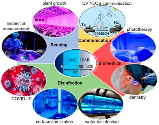
The electrically pumped (EP) and continuous-wave (CW) operating AlGaN-based diode lasers in the ultraviolet (UV)-B (320–280 nm) and UV-C (280–100 nm) wavelengths have significant potential in the four major application areas: free space non-line-of-sight communications [1], sensing [2], disinfection [3][4][5], and biomedicine [6][7]. A compilation of all the relevant applications in each area is shown in
The electrically pumped (EP) and continuous-wave (CW) operating AlGaN-based diode lasers in the ultraviolet (UV)-B (320–280 nm) and UV-C (280–100 nm) wavelengths have significant potential in the four major application areas: free space non-line-of-sight communications [1], sensing [2], disinfection [3,4,5], and biomedicine [6,7]. A compilation of all the relevant applications in each area is shown in
Figure 1. More recently, light sources operating at these wavelengths are discovered to be useful for sterilization of surfaces or objects, a necessary step to fight the global spread of coronavirus disease 2019 (COVID-19) [8][9]. While arguably some of these applications could be enabled by light-emitting diodes (LEDs), a wide range of applications of these UV-LEDs are limited due to their large-size, high-cost, and energy-inefficiency. Their advanced counterparts, e.g., lasers, however, show the promise of achieving low size, weight, power, and cost (SWaP-C) enabling devices [10]. Most importantly, lasers alleviate the light extraction and efficiency-droop constraints commonly found in III-nitride LEDs and extend their applications toward disinfection to air and large-surface sterilization at standoff distances because of their high-power density and light directionality.
. More recently, light sources operating at these wavelengths are discovered to be useful for sterilization of surfaces or objects, a necessary step to fight the global spread of coronavirus disease 2019 (COVID-19) [8,9]. While arguably some of these applications could be enabled by light-emitting diodes (LEDs), a wide range of applications of these UV-LEDs are limited due to their large-size, high-cost, and energy-inefficiency. Their advanced counterparts, e.g., lasers, however, show the promise of achieving low size, weight, power, and cost (SWaP-C) enabling devices [10]. Most importantly, lasers alleviate the light extraction and efficiency-droop constraints commonly found in III-nitride LEDs and extend their applications toward disinfection to air and large-surface sterilization at standoff distances because of their high-power density and light directionality.
Figure 1. Overview of various applications categorized into four major areas enabled by ultraviolet (UV)-B (320–280 nm) and UV-C (280–100 nm) lasers.

2. Overview of Recent Progress of AlGaN Ultraviolet (UV)-B and -C Lasers
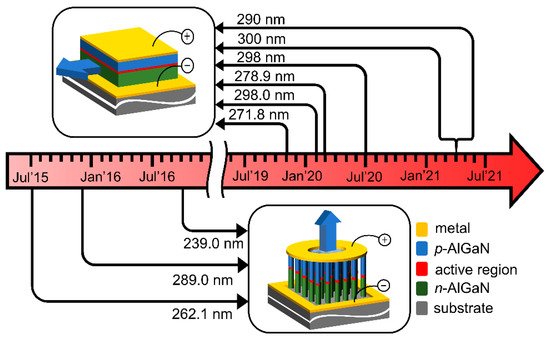
UV-B and -C LEDs have already successfully ensured reasonably good performance metrics. Hence, these devices are commercially available from a number of suppliers [11][12]. However, the additional complexity in terms of epi-structures [13][14], thicker layers [15][16][17] and higher crystalline quality [18][19][20] requirements have enabled achievement of lasers limited to only the UV-A wavelength span; which requires low-Al containing AlGaN heterostructures. For a long time until 2015, the shortest wavelengths reported for EP AlGaN-based UV lasers were 336 nm [21] and 334 nm [22] for thin films and NWs, respectively. The first-ever sub-300 nm EP AlGaN-based thin film-based lasers with an emission wavelength of 271.8 nm was demonstrated in 2019 [23]. Only four months after the first demonstration, pulse and RT operating UV-B lasers at 298 nm were reported [24]. Similarly, in reference [25], the authors presented laser devices emitting at ~279 nm by following the epi-layer design in reference [23] with lower threshold current density. Omori et al. reported the improvement in 298 nm UV-B laser performance [26] by employing a slightly different active region. The technological advances over time for EP UV-B and -C lasers are illustrated in
Overview of various applications categorized into four major areas enabled by ultraviolet (UV)-B (320–280 nm) and UV-C (280–100 nm) lasers.

2. Overview of Recent Progress of AlGaN Ultraviolet (UV)-B and -C Lasers

UV-B and -C LEDs have already successfully ensured reasonably good performance metrics. Hence, these devices are commercially available from a number of suppliers [51,52]. However, the additional complexity in terms of epi-structures [53,54], thicker layers [23,55,56] and higher crystalline quality [57,58,59] requirements have enabled achievement of lasers limited to only the UV-A wavelength span; which requires low-Al containing AlGaN heterostructures. For a long time until 2015, the shortest wavelengths reported for EP AlGaN-based UV lasers were 336 nm [60] and 334 nm [26] for thin films and NWs, respectively.
The first-ever sub-300 nm EP AlGaN-based thin film-based lasers with an emission wavelength of 271.8 nm was demonstrated in 2019 [30]. Only four months after the first demonstration, pulse and RT operating UV-B lasers at 298 nm were reported [31]. Similarly, in reference [33], the authors presented laser devices emitting at ~279 nm by following the epi-layer design in reference [30] with lower threshold current density. Omori et al. reported the improvement in 298 nm UV-B laser performance [32] by employing a slightly different active region. The technological advances over time for EP UV-B and -C lasers are illustrated in
Figure 2
.
Figure 2. All key demonstrations [27][28][29][23][24][26][25][30][31][32] for electrically-pumped AlGaN lasers covering ultraviolet (UV)-B and -C wavelengths since 2015.
Due to the unique ability of lateral stress relaxation associated with large surface area, developing high-quality AlGaN NWs has been quite successful with a wide range of Al compositions. In 2015, the first EP AlGaN based NW laser emitting at 262.1 nm was achieved [28]. Later in the same year, the same group demonstrated the EP AlGaN-based NW lasers, for the first time, at UV-B [27]. With further exploration, Zhao et al. reported RT operating EP AlGaN [29] based lasers at 239 nm in 2016 which, to date, is the lowest EP laser wavelength among all the thin film and NW-based devices.
All key demonstrations [27,28,29,30,31,32,33,34,35,36] for electrically-pumped AlGaN lasers covering ultraviolet (UV)-B and -C wavelengths since 2015.
Due to the unique ability of lateral stress relaxation associated with large surface area, developing high-quality AlGaN NWs has been quite successful with a wide range of Al compositions. In 2015, the first EP AlGaN based NW laser emitting at 262.1 nm was achieved [28]. Later in the same year, the same group demonstrated the EP AlGaN-based NW lasers, for the first time, at UV-B [27]. With further exploration, Zhao et al. reported RT operating EP AlGaN [29] based lasers at 239 nm in 2016 which, to date, is the lowest EP laser wavelength among all the thin film and NW-based devices.
Table 1
provides a summary of AlGaN lasers and their corresponding performance parameters demonstrated by different research teams in the world.
Table 1.
A brief summary of experimental realizations of AlGaN electrically pumped (EP) lasers listed based on the material types.
Reference Growth Method Material Type Lasing Wavelength (nm) Threshold (kA/cm2) Substrate Operating

Temp.
Operating Mode
Zhang et al., 2019 [23]Zhang et al., 2019 [30] MOCVD Thin film 271.8 25 AlN single crystal RT Pulse
Sato et al., 2020 [24]Sato et al., 2020 [31] MOCVD Thin film 298 41 AlN/sapphire RT Pulse
Sakai et al., 2020 [25]Sakai et al., 2020 [33] MOCVD Thin film 278.9 19.6 AlN single crystal RT Pulse
Omori et al., 2020 [26]Omori et al., 2020 [32] MOCVD Thin film 298 25 AlN/sapphire RT Pulse
Kushimoto et al., 2021 [30]Kushimoto et al., 2021 [34] MOCVD Thin film 271.2   AlN single crystal RT Pulse
Tanaka et al., 2021 [31]Tanaka et al., 2021 [35] MOCVD Thin film 300 13.3 AlN/sapphire RT Pulse
Tanaka et al., 2021 [32]Tanaka et al., 2021 [36] MOCVD Thin film 290 35 AlN/sapphire RT Pulse
Zhao et al., 2015 [28] MBE Nanowire 262.1 0.2 Si 77K CW
Zhao et al., 2015 [27] MBE Nanowire 289 0.3 Si RT CW
Zhao et al., 2016 [29] MBE Nanowire 239   Si RT CW
MOCVD = metalorganic chemical vapor deposition, MBE = molecular beam epitaxy, RT = room temperature, CW = continuous-wave.

3. Challenges of AlGaN UV-B/C Lasers

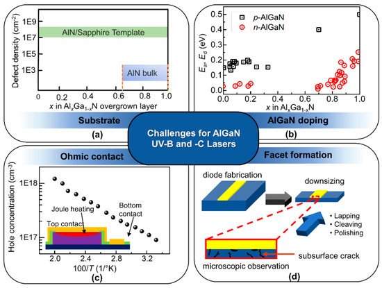
Figure 3
illustrates the major four challenges associated with the development of AlGaN laser technology.
Figure 3.
Four major challenges on the way towards demonstrating UV-B (320–280 nm) and UV-C (280–206 nm) lasers. (
a
) Current status of defect density in AlGaN films grown on AlN bulk substrate and AlN/sapphire template, (
b) the change of acceptor and donor activation energy for AlxGa1−xN with x [33][34][35][36][37][38][39], (
) the change of acceptor and donor activation energy for AlxGa1−xN with x [69,70,71,72,73,74,75], (
c) the high temperature requirement to achieve adequate hole concentration makes it challenging to achieve low resistive ohmic contacts [40]. Joule heating effect due to high contact resistance is shown in the inset, and (
) the high temperature requirement to achieve adequate hole concentration makes it challenging to achieve low resistive ohmic contacts [76]. Joule heating effect due to high contact resistance is shown in the inset, and (
d
) subsurface crack generation during facet formation. Figure (
c) is reproduced with permission from reference [40]. Copyright (1998) Elsevier B.V.

3.1. Substrates and Defects

AlN templates with low dislocation density and point defects are essential to enhance the emission efficiency of UV lasers. Nearly 80 times improvement in IQE was reported for AlGaN QW grown on AlN/sapphire templates with a TDD of 5 × 10
) is reproduced with permission from reference [76]. Copyright (1998) Elsevier B.V.

3.1. Substrates and Defects

AlN templates with low dislocation density and point defects are essential to enhance the emission efficiency of UV lasers. Nearly 80 times improvement in IQE was reported for AlGaN QW grown on AlN/sapphire templates with a TDD of 5 × 10
8
cm
−2
compared to those grown on conventional templates with TDDs 2 × 10
10
cm
−2 [41][42][43]. Due to the employment of different growth techniques such as HTA-sputtered AlN, epitaxial lateral overgrowth (ELO), patterned sapphire substrate (PSS) and thick AlN layer growth, significant advancement was made on AlN/sapphire over the years [44][45][46][47]. This led to TDDs in the range of 10
[61,62,63]. Due to the employment of different growth techniques such as HTA-sputtered AlN, epitaxial lateral overgrowth (ELO), patterned sapphire substrate (PSS) and thick AlN layer growth, significant advancement was made on AlN/sapphire over the years [64,65,66,67]. This led to TDDs in the range of 10
7
–10
9
cm
−2
. Using AlN bulk substrate which has a very low defect density in the range of 10
3
–10
4
cm
−2 has been quite popular for obtaining high-quality epilayers [23][48].

3.2. P- and N-Doping for High-Al

As UV-B and -C lasers require high-quality, low-defect and thick AlGaN cladding layers for improved waveguiding [49][50], their electrical performance is equally important. To achieve the high current density required in the active regions for laser operation, cladding layers need to be conductive which is particularly challenging for p-type doping for all x of AlxGa1−xN, as shown in
has been quite popular for obtaining high-quality epilayers [30,68].

3.2. P- and N-Doping for High-Al

As UV-B and -C lasers require high-quality, low-defect and thick AlGaN cladding layers for improved waveguiding [24,85], their electrical performance is equally important. To achieve the high current density required in the active regions for laser operation, cladding layers need to be conductive which is particularly challenging for p-type doping for all x of AlxGa1−xN, as shown in
Figure 3b [36]. Behind ineffective p-doping, the most formidable challenges include large acceptor ionization energy for Mg dopants in AlGaN [51][52], formation of low energies by compensating defects (donors) like nitrogen vacancies [53], limitation of solubility of Mg in AlGaN [35][54], hydrogen passivation of the Mg dopants [34][55] and the existence of parasitic impurities, such as hydrogen (H), carbon (C) and oxygen (O) [33][56][57]. Compared to p-type doping, n-type doping is easily attainable and Si-doped AlGaN up to x = 0.8 with a reasonable doping concentration was achieved [37][38][39]. However, a sharp increase in resistance was observed due to the high activation energy of Si which increases exponentially from 25 meV–250 meV once the x > 0.8 for n-AlxGa1−xN [37]. On top of this, the presence of compensating impurities carbon and oxygen in AlN substrates as well as MOCVD reactor impurities decrease donor concentrations in AlGaN with x > 0.85 by an order of magnitude [48][56][58].

3.3. Low-Resistive Ohmic Contact

b [72]. Behind ineffective p-doping, the most formidable challenges include large acceptor ionization energy for Mg dopants in AlGaN [86,87], formation of low energies by compensating defects (donors) like nitrogen vacancies [88], limitation of solubility of Mg in AlGaN [71,89], hydrogen passivation of the Mg dopants [70,90] and the existence of parasitic impurities, such as hydrogen (H), carbon (C) and oxygen (O) [69,91,92]. Compared to p-type doping, n-type doping is easily attainable and Si-doped AlGaN up to x = 0.8 with a reasonable doping concentration was achieved [73,74,75]. However, a sharp increase in resistance was observed due to the high activation energy of Si which increases exponentially from 25 meV–250 meV once the x > 0.8 for n-AlxGa1−xN [73]. On top of this, the presence of compensating impurities carbon and oxygen in AlN substrates as well as MOCVD reactor impurities decrease donor concentrations in AlGaN with x > 0.85 by an order of magnitude [68,91,93].

3.3. Low-Resistive Ohmic Contact

Figure 3c shows the representative AlGaN lasers with co-planar or intracavity contacts, which is the only possible way to form bottom n-side contacts. As the improvement in n- and p-type conductivity in Al-rich AlGaN continues, the low resistive ohmic contact realization emerges.

3.4. Facet Formation

Unlike the other III–V compound semiconductor-based lasers, III-nitride materials provide a reflectivity of only ~19% from the naturally cleaved facet at the semiconductor–air interface. This may necessitate a high-reflection coating on one of the facets in order to overcome resonator losses and obtain lasing, as schematically shown in
c shows the representative AlGaN lasers with co-planar or intracavity contacts, which is the only possible way to form bottom n-side contacts. As the improvement in n- and p-type conductivity in Al-rich AlGaN continues, the low resistive ohmic contact realization emerges.

3.4. Facet Formation

Unlike the other III–V compound semiconductor-based lasers, III-nitride materials provide a reflectivity of only ~19% from the naturally cleaved facet at the semiconductor–air interface. This may necessitate a high-reflection coating on one of the facets in order to overcome resonator losses and obtain lasing, as schematically shown in
Figure 3d. Another issue is that both sapphire and AlN are extremely hard materials. Hence, backend processes including substrate lapping and laser scribing to obtain mirror-finish facets pose many technical challenges to complete laser fabrication [59][60]. One sometimes breaks processed lasers and polishes the cavity-ends to obtain high-quality facets, which, however, increases manufacturing cost.

4. Critical Technical Areas for AlGaN UV-B and -C Lasers
d. Another issue is that both sapphire and AlN are extremely hard materials. Hence, backend processes including substrate lapping and laser scribing to obtain mirror-finish facets pose many technical challenges to complete laser fabrication [98,99]. One sometimes breaks processed lasers and polishes the cavity-ends to obtain high-quality facets, which, however, increases manufacturing cost.

4. Critical Technical Areas for AlGaN UV-B and -C Lasers

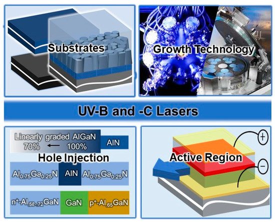
Figure 4
schematically shows the four major technical pillars that will determine the success of UV-B and -C laser technology and underpin the implementation of high-performance AlGaN devices.
Figure 4.
Major technical pillars determining the success of UV-B and UV-C laser technology.

4.1. Substrate Materials

Figure 5 schematically shows all the possible substrates that are used for implementing EP AlGaN lasers.

Figure 5.
Possible substrate options for thin film and NW-based full UV-B (320–280 nm) and partial UV-C (280–206 nm) lasers. (
a
,
b
) represents the bulk substrates AlN and Si, respectively. (
c
) schematically shows the AlGaN thin film samples grown on HTA-AlN template. (
d
,
e
) demonstrates newly developed two-step growth templates with self-nucleating 3D AlN growth and periodic concavo-convex pattern AlN, respectively.

4.2. Growth Technology

The two most popular methods available for epitaxial growth AlGaN UV laser materials are molecular beam epitaxy (MBE) [61][62][63][64][128,131,132,133] and metalorganic chemical vapor deposition (MOCVD) [65][66][67][134,135,136]. When it comes to templated substrates, MOCVD is superior to MBE for growing high-quality AlN templates due to high growth-temperatures and -rates [68][69][70][137,138,139].

Although not as extensive as MOCVD, MBE-grown UV materials, i.e., both thin film and NWs, have also been studied over the years. As a matter of fact, MBE offers some distinct benefits over MOCVD in terms of interface diffusion, defect control, memory effect, high hole concentration in p-AlGaN, Mg passivation and significant control over defect incorporation [71][143]. Due to its relatively low growth temperature MBE grown samples do not suffer from surface damage due to chemical reaction at high temperature often associated with MOCVD. This suggests the superiority of MBE over MOCVD in terms of growing high-quality active regions.

Lasers with buried TJ may require a hybrid MOCVD/MBE growth approach [72][73][147,148]. In such structures, a base structure, containing all the layers up to an active region and the p+-side of the TJ, is grown by MOCVD, and the remainder of the device including the n+-side of TJs, n-cladding and n+-contact layers can be overgrown during the second epitaxial growth by MBE. Hence, the hybrid approach, comprising a MOCVD-grown base structure with the active region and MBE-grown TJs, is another viable alternative towards obtaining high-performance UV-B and -C lasers.

4.3. Three Major Techniques for Hole Injection

4.3.1. Distributed Polarization Doping

Introducing dopants in AlGaN by compositionally grading, commonly addressed as DPD takes advantage of both spontaneous and piezoelectric polarization. Since its first demonstration, DPD has been widely popular as an effective means to enhance p-AlGaN doping [74][153].Figure 6a shows how compositionally graded AlGaN creates polarization-induced 3D charges that result in free carriers. 
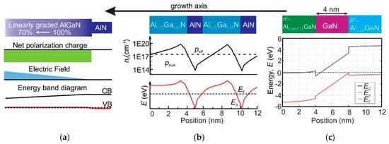
Figure 6.
Schematic representation of the p-doping process; (
a
) schematic representation of distributed polarization doping (DPD) process for an AlGaN layer graded from x = 0.7 to 1, (
b
) a schematic representation of short-period superlattice (SPSL) with Al0.75Ga0.25N/AlN alternate layers doped with 3.5 × 10
19
cm
−3
Mg generated. The dotted line represents the hole concentration for bulk Al0.75Ga0.25N with equal doping, and (
c
) band diagram of a p-AlGaN/i-InGAN/n-AlGaN TJ.

4.3.2. Short-Period Superlattice

A short-period superlattice, comprising of alternate layers of AlxGa1−xN with high and low x doped with Mg (AlxGa1−xN/AlyGa1−yN with x > y) was used to improve hole activation with the help of band offset and strong built-in spontaneous and piezoelectric polarization fields instead of thermal energy [75][76][77][78][158,159,160,161]. By improving vertical conductivity, the resistance of an SPSL reduced nearly 12 times compared to a bulk layer with the same composition, making the SPSL layer suitable to operate at a high voltage [17][56].

4.3.3. Tunnel Junctions (TJs)

With the help of polarization doping, successful demonstration of GaN-based TJ was reported since 2001 [79][162] and in 2016 the first AlGaN based TJ was reported [80][163]. While p-AlGaN is necessary for p-side cladding, implementing a TJ eliminates the thick p-cladding layer requirement. The use of TJs as an intracavity contact for hole injection through interband tunneling is reported in a number of experimental studies [16][81][82][83][84][55,150,151,164,165].

4.4. Active Region

For the successful design and demonstrations of UV-B and -C lasers, one primarily requires a good AlGaN-based active region to obtain high material gain [85][13][86][22,53,154]. This includes not only a good material quality with low-defects and sharp interfaces but also an optimal number of QWs, and the right thicknesses of QWs and barrier with optimal band offsets and adjusting the waveguide thickness [87][88][89][16,167,168]. These considerations will be added by the polarization switching phenomena of emitted light for the unique AlGaN material system [90][91][169,170]. Using a higher number of QWs appears to be non-conventional in the wavelengths of interest due to the constraint of uniform pumping of all the QWs with carriers to obtain material gain. If one of the quantum wells cannot be pumped enough, they will operate as a band-edge absorbing layer and then it fails to lase.

5. Demonstration of AlGaN Lasers

5.1. Thin Film Lasers

In 2019, the first thin film-based EP AlGaN laser at UV-C was achieved by researchers at Nagoya University, Japan, in cooperation with Asahi Kasei Corporation, Chiyoda City, Japan and Crystal IS, Inc., Green Island, NY, USA [23]. The laser materials were pseudomorphically grown on (0001) bulk AlN substrates by MOCVD. The devices used a single AlGaN 9-nm-thick QW to emit at 271.8 nm. For hole injection, pseudomorphic DPD layers were used on top of p-waveguide.

5. Demonstration of AlGaN Lasers

5.1. Thin Film Lasers

In 2019, the first thin film-based EP AlGaN laser at UV-C was achieved by researchers at Nagoya University, Japan, in cooperation with Asahi Kasei Corporation, Chiyoda City, Japan and Crystal IS, Inc., Green Island, NY, USA [30]. The laser materials were pseudomorphically grown on (0001) bulk AlN substrates by MOCVD. The devices used a single AlGaN 9-nm-thick QW to emit at 271.8 nm. For hole injection, pseudomorphic DPD layers were used on top of p-waveguide.

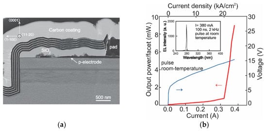
Figure 7

a schematically shows the fully processed FP lasers.
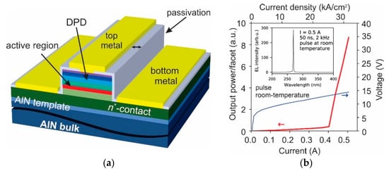
Figure 7.
(
a
) Schematic cross-section of fully-processed UV-C laser and (
b
) its L-I-V characteristics. (
b) is reproduced with permission from reference [23]. Copyright (2019) The Japan Society of Applied Physics.
The same research team engineered the same laser epilayers by combining dry and wet etching [92][93][94] to form smooth-vertical sidewalls on mirror facets [25]. The facets were then coated with a distributed Bragg reflector (DBR) composed of HfO2 and Al2O3, yielded 49.6% reflectivity. This significantly reduced the threshold current density of the device [95]. A cross-sectional scanning electron microscopy image with DBR coating is shown in
) is reproduced with permission from reference [30]. Copyright (2019) The Japan Society of Applied Physics.
The same research team engineered the same laser epilayers by combining dry and wet etching [172,173,174] to form smooth-vertical sidewalls on mirror facets [33]. The facets were then coated with a distributed Bragg reflector (DBR) composed of HfO2 and Al2O3, yielded 49.6% reflectivity. This significantly reduced the threshold current density of the device [175]. A cross-sectional scanning electron microscopy image with DBR coating is shown in
Figure 8
a.
Figure 8.
(
a
) Scanning electron microscopy (SEM) cross-section of UV-C laser with vertical sidewalls and distributed Bragg reflector (DBR) coating, and (
b) and its L-I-V characteristics. The lasing spectrum is shown in the inset. Figures are reproduced with permission from Reference [25]. Copyright (2020) AIP Publishing LLC.

5.2. Nanowire Lasers

Three experimental demonstrations of NW-based EP AlGaN lasers in the wavelengths of interest are reported so far [27][28][29]. All of these three reports were made by the same research group from McGill University, Canada. The type of cavity adopted in all these studies used random NW arrays, yielding random lasing [96][97].
) and its L-I-V characteristics. The lasing spectrum is shown in the inset. Figures are reproduced with permission from Reference [33]. Copyright (2020) AIP Publishing LLC.

5.2. Nanowire Lasers

Three experimental demonstrations of NW-based EP AlGaN lasers in the wavelengths of interest are reported so far [27,28,29]. All of these three reports were made by the same research group from McGill University, Canada. The type of cavity adopted in all these studies used random NW arrays, yielding random lasing [179,180].
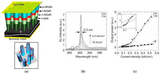
Figure 9a shows the schematic of AlGaN NW array lasers. The NW structure consisted of GaN:Si (∼250 nm), AlGaN:Si (∼100 nm), AlGaN (∼100 nm), AlGaN:Mg (∼100 nm), and GaN:Mg (∼10 nm) segments. The devices were designed to act as surface-emitting lasers although there was ~20 nm-thick metal p-contact on the top with negligible absorption.
Photonics 08 00267 g012 550
12a shows the schematic of AlGaN NW array lasers. The NW structure consisted of GaN:Si (∼250 nm), AlGaN:Si (∼100 nm), AlGaN (∼100 nm), AlGaN:Mg (∼100 nm), and GaN:Mg (∼10 nm) segments. The devices were designed to act as surface-emitting lasers although there was ~20 nm-thick metal p-contact on the top with negligible absorption.
Figure 912.
(
a
) Three-dimensional schematic representation of the fully-processed random lasers. Inset shows the mechanism for random laser emission, (
b
) electroluminescence (EL) emission spectra measured under different current densities, and (
c
) integrated EL intensity as a function of the injection current for the NW laser. Figures are reproduced with permission from Reference [28]. Copyright (2015) AIP Publishing LLC.
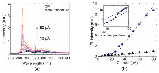
Again a few months later, UV-B lasing from single-crystalline AlGaN NWs was demonstrated by the same research team from McGill University [27].
Figure 10a shows the current dependent EL spectra with a peak at 289 nm. The extracted L-I characteristics of the random lasers are presented in
3a shows the current dependent EL spectra with a peak at 289 nm. The extracted L-I characteristics of the random lasers are presented in
Figure 10b. Owing to the optimized 3D optical confinement structure, the threshold current density reduced to 0.3 kA/cm
3b. Owing to the optimized 3D optical confinement structure, the threshold current density reduced to 0.3 kA/cm
2
under CW operation. The lasing area was 10 µm
2
.
Figure 103.
UV-C lasing characteristics at RT, (
a
) EL emission spectra measured under different current densities, and (
b
) integrated EL intensity as a function of the injection current. Figures are reproduced with permission from reference [27]. Copyright (2015) AIP Publishing LLC.
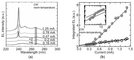
Figure 11a shows the applied current-dependent EL spectra with much shorter linewidth compared to the previously reported results. RT and CW operation was observed from the devices. This is the shortest wavelength reported to date for any EP AlGaN laser.
4a shows the applied current-dependent EL spectra with much shorter linewidth compared to the previously reported results. RT and CW operation was observed from the devices. This is the shortest wavelength reported to date for any EP AlGaN laser.
Figure 11b shows the extracted L-I characteristics for the random lasers at 239 nm.
Photonics 08 00267 g014 550
4b shows the extracted L-I characteristics for the random lasers at 239 nm.
Figure 114.
UV-B lasing characteristics at room temperature (RT) (
a
) the EL emission spectra measured under different current density, and (
b) integrated EL intensity as a function of the injection current density. Figures are reproduced with permission from reference [29]. Copyright (2016) AIP Publishing LLC.
) integrated EL intensity as a function of the injection current density. Figures are reproduced with permission from reference [29]. Copyright (2016) AIP Publishing LLC.
Video Production Service